downloadGroupGroupnoun_press release_995423_000000 copyGroupnoun_Feed_96767_000000Group 19noun_pictures_1817522_000000Member company iconResource item iconStore item iconGroup 19Group 19noun_Photo_2085192_000000 Copynoun_presentation_2096081_000000Group 19Group Copy 7noun_webinar_692730_000000Path
Skip to main content
Default Banner Image

United States

United States Understanding Semiconductor Technology and Business Training
Highlighted content

Course Description

The first part of the course provides a brief overview of semiconductor design and fabrication steps, encompassing IC design techniques, all wafer processing steps, assembly, and packaging. It delves into semiconductor jargon in laypeople terms, and various substrate types such as Si, SiGe, FDSOI, GaAs, SiC, GaN. Additionally, it discusses different types of transistors like pMOS, nMOS, Bipolar, BiCMOS, CMOS, FinFets, and GAA and their evolution and what applications they are used in.
 
The second part of the course focuses on semiconductor business aspects such as silicon economics, wafer processing costs, semiconductor revenue forecasts, driving forces in the industry, top semiconductor IDMs, market competitors based on market share, OEMs, foundries, top tool vendors, and Fabless companies.  Addresses the fastest-growing semiconductor markets based on geographic locations and applications, identifies semiconductor competitors/customers, and discusses major semiconductor markets like Automotive, PC, Mobile, Memory, Wireless, Cell phones, Consumer, Gaming, AI, IoT, Digital TV, Radio, Automotive, MEMS, and Emerging Technology & Impact on Industry.

Learning Objectives

  • Understand the fundamental principles and theories semiconductor technology.
  • Communicate with other associates and understand wafer processing steps.
  • Understand semiconductor business aspects such as silicon economics, wafer processing costs, semiconductor revenue forecasts, driving forces in the industry, top semiconductor IDMs, market competitors based on market share, OEMs, foundries, top tool vendors, and Fabless companies.
  • Review the semiconductor eco-system as it relates to design and fabrication of a semiconductor device.
  • Gain knowledge of major semiconductor markets like Automotive, PC, Mobile, Memory, Wireless, Cell phones, Consumer, Gaming, AI, IoT, Automotive, MEMS, and Emerging Technology & Impact on Industry.
  • Demonstrate effective communication skills through written reports, presentations, and discussions related to semiconductor subjects.
  • Collaborate effectively with peers in group projects or discussions regarding semiconductor subjects.
  • Analyze and evaluate research literature in semiconductor technology.
  • Develop critical thinking and problem-solving skills applicable to semiconductor technology.

Who Should Attend

This course is suitable for anyone seeking a better understanding of the semiconductor industry, market leaders, terminology, business, and the semiconductor ecosystem.

Instructor

Denny Frye 

PT International, LLC

Instructor Bio
 

Important Information

Note that only the person who registered will receive a certificate of completion. This virtual training will not be recorded. Attendees must be present to access course knowledge. 

Can't find the training link day of? After you register, you will receive the link to the live training via the email address you provided. In addition, you will receive email reminders about 24 hours in an advance and an hour before with the same link. Please keep these emails on hand to access the trainings on time. If you do not see any confirmation emails, please check your junk/spam folders before contacting SEMI U for support. 

United States

SEMI U

Embark on a journey through semiconductor design, manufacturing, and business in this illuminating course. Explore IC design techniques, transistor evolution, and market dynamics. Delve into substrate types and industry economics, discovering the fastest-growing markets and key players shaping the semiconductor landscape.

Pricing
  • Members: $845
  • Non-Members: $945

* For group orders with 10+ attendees, and for Students/Veterans discounted pricing, please contact [email protected].
9:30 am - 5:00 pm Off Add to Calendar 2025-06-02 09:30:00 2025-06-02 17:00:00 Understanding Semiconductor Technology and Business (Virtual Training, US) Embark on a journey through semiconductor design, manufacturing, and business in this illuminating course. Explore IC design techniques, transistor evolution, and market dynamics. Delve into substrate types and industry economics, discovering the fastest-growing markets and key players shaping the semiconductor landscape.PricingMembers: $845Non-Members: $945* For group orders with 10+ attendees, and for Students/Veterans discounted pricing, please contact [email protected]. United States SEMI.org [email protected] America/Los_Angeles public America/Los_Angeles Closed

Event format
Promote in calendar
Off

Regular Pricing

Members: $475

Non-Members: $590

Students: $99

  • Breakfast, Breaks, Lunches
  • Networking Reception
  • Design Skills-Building Workshop (Pre-Event)
  • Intel Museum Tour and Transportation
  • Lunch & Learn Packet (Post-Conference Distribution)
  • Proceedings (Post-Conference Distribution)

Note: Travel-related expenses are not included.

Cancellations received on or before August 16, 2025 are fully refunded with a $100 processing fee.  Refunds will not be issued for cancellations (including no-shows) made after August 16, 2025, and only substitutions are accepted with a written note from the registered attendee.  Please email your cancellations or substitutions on company letterhead to:

Michelle Fabiano
Sr. Manager, Programs & Committees
[email protected]

+
United States MEMS & Sensors NextGen 360x317x NEW Business Technical

Travel

Local Hotels Near SEMI HQ:

Embassy Suites by Hilton Milpitas Silicon Valley
901 East Calaveras Boulevard
Milpitas, CA 95035
+1 (408) 942-0400

Courtyard by Marriott Milpitas Silicon Valley
1480 Falcon Dr.
Milpitas, CA 95035
+1 (408) 719-1966

Robert Bosch Logo 170x65
Consulate General of Canada Logo 170x65
Lam Research
Silex Microsystems Logo 170x65
TDK Logo 170x65
Teledyne MEMS Logo 170x65


BECOME A SPONSOR FOR MSNG 2025!

Sponsorship opportunities can be tailored to meet your specific branding and marketing objectives.

View our Sponsorship Brochure

Contact Tim Janes | [email protected] | +1 720-939-4992


Industry & Media Partners

SEMI is proud to partner with the following media and associations to bring you news about this event. Click below to read, subscribe, or visit their website to learn more about each of them.


Speakers represent the MEMS and sensors supply chain and adjacent industries. The conference will explore cutting-edge topics including photonics, digital twins and AI, machine learning, environmental sensors, quantum sensors, entrepreneurialism, innovation and collaboration. The programming is curated to appeal to the “NextGen” MEMS and sensors professionals through programming features of the conference that include networking, problem-solving, and skill development.


TOPICS

Gain insights as we dive into the following topics:

  • Environmental Sensors
  • Innovation
  • Photonics MEMS and Sensing Technology
  • Quantum Sensors
  • Digital Twins and AI for MEMS Design
  • AI & Machine Learning in MEMS and Sensor Device Operation


WHO SHOULD ATTEND

This conference is open to all MEMS & sensors professionals interested in NextGen technology.

  • Technologists​
  • Engineers ​
  • Startups | Founders
  • Academia | Students | Professors ​
  • Market Analysts | Market Researchers
  • Investors: VCs | Angel Investors | MEMS and Sensors Technology Investors


EVENT CONTACT

Michelle Fabiano
Sr Manager, Programs & Committees
[email protected]
 

SPONSORSHIP OPPORTUNITIES

Tim Janes 
Account Manager, Events 
[email protected]


MSNG 2025 PLANNING ALLIANCE

Thank you to these industry leaders for their time, expertise, and support of the MSNG conference.
 

SEMI HQ
673 South Milpitas Boulevard​
Seminars 1 & 2​
Milpitas, CA 95035
United States

TUESDAY, SEPTEMBER 16, 2025

1:30 pm - 2:20 pm

Registration

2:20 pm
Paul Carey
Paul Carey
Director, MSIG
SEMI Americas

Welcome Remarks

2:30 pm - 5:30 pm

MEMS Design Workshop: Unlock the Future of MEMS Design with Cloud-Native Multiphysics Simulation

Gerry Harvey Headshot
Gerry Harvey
Quanscient

Instructor

Abhishek Deshmukh, Quanscient
Abhishek Deshmukh
Quanscient

Instructor

Alex Stockrahm
Quanscient

Instructor

WEDNESDAY, SEPTEMBER 17, 2025

7:30 am - 8:30 am

Registration & Breakfast

8:30 am - 8:40 am
Paul Carey
Paul Carey
Director, MSIG
SEMI Americas

Welcome Remarks

8:40 am - 9:10 am
David Horsley, Institute of NanoSystems Innovation, Northeastern University
David Horsley
Professor, Startup Founder, Advisor & Angel Investor
Institute for NanoSystems Innovation, Northeastern University

Keynote—Crossing the Chasm: from Academic Lab to Consumer Pockets

Session 1— Environmental Sensors & Monitoring

Session Sponsor—TDK USA

TDK Logo 170x65
9:10 am
Pierre-Damien Berger, CEA Leti
Pierre-Damien Berger
MEMS Industrial Partnerships Manager
CEA Leti

Session Chair Welcome

9:15 am
Nishit Goel, TDK USA
Nishit Goel, PhD
Senior Staff Engineer
TDK USA

Fragrance Sensing for a Fragmented Market

9:40 am
Shiyao Shan_GE
Shiyao (Shawn) Shan, PhD
Lead Engineer
GE Vernova Advanced Research Center

System Approach in Boosting Sensitivity, Selectivity, and Stability of Modern Environmental and Industrial Gas sensors to Deliver Broad Societal Impact

10:05 am - 10:35 am

Networking Break

Session 2—Universities & Industry Enabling Innovation: Panel Discussion

Presented by the Consulate General of Canada in San Francisco

Consulate General of Canada Logo 170x65
10:35 am
John Busch, Berkeley Skydeck
John Busch
Co-Chair
Berkeley Skydeck

Moderator

10:40 am - 10:45 am
Rahul Devaskar, Canadian Consulate of San Francisco
Rahul Devaskar
Senior Investment Officer
Canadian Consulate of San Francisco, and Silicon Valley

Consulate General of Canada Sponsor Message

Philippe Lanctôt Headshot
Philippe Lanctôt
Director of Business Development
C2MI
Michelle Kiang, MTM Ventures
Michelle Meng-Hsiung Kiang
Founder
MTM Ventures
Bharath Rajagopalan, STMicroelectronics
Bharath Rajagopalan
Director, Strategic Market Development
STMicroelectronics
Valentin Antoine, TDK
Valentin Antoine
Investment Analyst
TDK Ventures
11:45 am - 1:00 pm

Networking Lunch

Session 3—Photonics MEMS and Sensing Technology

1:00 pm
Anson Yeganegi, TDK USA
Anson Yeganegi
Director of Business Development
TDK USA

Session Chair Welcome

1:05 pm
Kevin Yasumura, Google
Kevin Yasumura
Principal Engineer | Director of MEMS and Optical Switching Development
Google

MEMS Optical Circuit Switching for AI Applications

1:30 pm
Lia Li,  Zero Point Motion
Ying Lia Li
CEO
Zero Point Motion

MEMS Reimagined: Photonic Readout and On-Chip Compute for Inertial Sensing

1:55 pm
Pierre-Damien Berger, CEA Leti
Pierre-Damien Berger
MEMS Industrial Partnerships Manager
CEA Leti

Enabling High Efficiency Sensing with Optomechanical Devices

2:20 pm
Pierre Delbos_Yole Group
Pierre Delbos
Business Development Manager
EV Group

From Concept to Market: Manufacturing Platforms for Next-Gen Photonic MEMS

2:45 pm - 3:15 pm

Networking Break

Sponsor—Bosch

Robert Bosch Logo 170x65

Session 4—Pioneer Pitch: Sensors & Startups

3:15 pm
Marcellino Gemelli, Robert Bosch LLC
Marcellino Gemelli
Business Development, Bosch Sensortec GmbH
Robert Bosch

Session Chair Welcome

3:20 pm

Pioneer Pitch: Sensors & Startups

Jaehyung James Lee
Jaehyung James Lee
Co-founder and CEO
Stratio Technology

Unlocking the Power of SWIR: Ge-based SWIR Sensors and Infrared-AI for Breakthrough Industrial Applications

Jérôme Michon_InSpek
Jérôme Michon
Co-founder and CEO
InSpek

InSpek: OneProbe, Multiple Sensors

Ramesh Chandrasekhar, Aynak
Ramesh Chandrasekhar
CEO and Founder
Aynak

Sensory Eyewear: Designed to Hear, Crafted to be Seen

William Xander, Truthkeep
William Xander
CEO and Founder
Truthkeep

The Missing Piece of Your Strategic Advantage

Saewook Lee, Applied Ventures
Saewook Lee
Senior Director
Applied Ventures

Venture Capitalist

David Lam Headshot
David Lam
Senior Advisor
BRV Capital Management
Michelle Kiang, MTM Ventures
Michelle Meng-Hsiung Kiang
Founder
MTM Ventures

Paul Pickering, Silicon Catalyst
Paul Pickering
Managing Partner
Silicon Catalyst
5:00 pm - 6:30 pm

Networking Reception with Group Introductions & Student Poster Session

Sponsor—SILEX

Silex Microsystems Logo 170x65

THURSDAY, SEPTEMBER 18, 2025

7:30 am - 8:30 am

Registration & Breakfast

8:30 am
Paul Carey
Paul Carey
Director, MSIG
SEMI Americas

Welcome Remarks

8:35 am
Marcellino Gemelli, Robert Bosch LLC
Marcellino Gemelli
Business Development, Bosch Sensortec GmbH
Robert Bosch LLC

Keynote—A Novel Customer Discovery Approach for Sensor Submodules in Distribution Channels

Session 5—Quantum Sensors

9:05 am
Pierre Delbos_Yole Group
Pierre Delbos
Business Development Manager
EV Group

Session Chair Welcome

9:10 am
Amirhossein Ghods, Mesa Quantum
Amirhossein Ghods
Vice President of Photonics
Mesa Quantum

Advanced VCSELs for Scalable Quantum Sensing Applications

9:35 am
Christopher Chua
Christopher Chua
Associate Director & Principal Research Scientist
SRI

Narrow Linewidth PIC-based Blue-UV Semiconductor Lasers for Optical Atomic Clocks

10:00 am
Paul Morton, Headshot
Paul Morton
CTO Photonics
Infleqtion

Photonic Integration for Miniaturization of a 2-photon Rb Optical Atomic Clock

10:25 am - 10:55 am

Networking Break

Session 6—Digital Twins and AI for MEMS Design

10:55 am
Benyamin Davaji, Northeastern University
Benyamin Davaji, PhD
Assistant Professor
Northeastern University

Session Chair Welcome

11:00 am
Prith Banerjee
Prith Banerjee
Senior Vice President, Simulation and Analysis Incubation
Synopsys

Challenges & Opportunities of Digital Twins in Asset-Intensive Industries

11:25 am
Andy Cai, COMSOL
Andy Cai
Applications Manager
COMSOL, Inc.

Digital Twins and Simulation Apps

11:50 am
Michael Munsey Headshot
Michael Munsey
Vice President Semiconductor and Electronics Industries
Siemens Digital Industries Software

Creating the Digital Twin for Semiconductor Design to Manufacturing

12:15 pm - 1:30 pm

Networking Lunch

Sponsor—Teledyne MEMS

Teledyne MEMS Logo 170x65

Session 7—AI & Machine Learning in MEMS & Sensor Device Operation

1:30 pm
Mary Ann Maher, SoftMEMS
Mary Ann Maher
CEO
SoftMEMS

Session Chair Welcome

1:35 pm
Juan Mejia Santamaria, TDK
Juan Mejia Santamaria
Principal Engineer and Team Lead
TDK USA Corporation

Going Beyond Sensors Everywhere

2:00 pm
Jonathan Russo, Femtosense Headshot
Jonathan Russo
Program Manager
Femtosense

AI Speech Enhancement and the Future of Hearables

2:25 pm
Nathan Francis, Headshot
Nathan Francis
Head of Business Development
AI Zip

From Data to Decisions: Smart MEMS with Local AI Processing

2:50 pm
Paul Carey
Paul Carey
Director, MSIG
SEMI Americas

Closing Remarks & Introduction to the Tour

3:00 pm - 6:30 pm

Computer History Museum Tour

The Computer History Museum (CHM) is a computer museum in Mountain View, California. The museum presents stories and artifacts of Silicon Valley and the Information Age, and explores the computing revolution and its impact on society. Transportation will be provided.

- MSIG Workforce Development

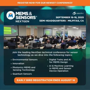
MEMS & Sensors NextGen—MSNG 2025 is the leading NextGen sensor technology technical conference for NextGen professionals related to designing, building, and using sensors. 

2:30 pm - 6:30 pm Off Add to Calendar 2025-09-16 14:30:00 2025-09-18 18:30:00 MEMS & Sensors NextGen MEMS & Sensors NextGen—MSNG 2025 is the leading NextGen sensor technology technical conference for NextGen professionals related to designing, building, and using sensors.  SEMI HQ 673 South Milpitas Boulevard​ Seminars 1 & 2​ Milpitas, CA 95035 United States SEMI.org [email protected] America/Los_Angeles public America/Los_Angeles

Share on LinkedIn

MSNG 2025 SoMe Post Early Bird Registration, 300x300

Let your LinkedIn connections know you’re attending MSNG! 

Spread the word and share our social media content with your connections so that they can join you there, too.

MSNG 2025 SoMe Post Early Bird Registration, 300x300
Register Now
Event format
Promote in calendar
Off

REGISTRATION

Attendance is free, but registration is required by March 10, 2025.

United States PDS Generic Thumbnail 690x448x

SEMI Professional Development Seminar—Connecting College Students to the Semiconductor Industry 

Learn about career opportunities in high tech and acquire valuable, practical information that will help you choose career directions and plan for your success.

Come learn about careers in the semiconductor industry at the SEMI Professional Development Seminar hosted by Missouri S&T.

  • Listen to professionals in the industry talk about their roles and find out how to prepare for jobs in the Semiconductors Industry. 
  • Discover semiconductor job opportunities you didn't know existed (internship and entry-level) and how you can prepare for them through job searches, interviews, resumes, and more.
  • Meet with professionals and executives during our speed mentoring, mock interview, and networking sessions.

All majors are welcome! Students with a background in Engineering, Computer Science, Chemistry, Physics, Math, Data Science, and Business are strongly encouraged to attend.

  • Enjoy free food, free swag, and giveaways.
  • Students can come and go.

EVENT is FREE but registration is required. Registration deadline coming soon! 

Missouri University of Science and Technology
MO
United States

MONDAY, MARCH 17, 2025 (Times in CST)

9:00 am - 9:30 am

Check-In

9:30 am - 9:40 am
David Borrok
Missouri S&T

Welcome

9:30 am - 9:40 am
Mike Seacrist
MEMC

SEMI Midwest Chapter Introduction

9:40 am - 10:00 am
David Lipke
Missouri S&T

Missouri S&T Educational Opportunities

10:00 am - 10:20 am
Joyce Lowes
Director, R&D Emerging Materials Group
Brewer Science

Semiconductors 101: A Brief History of the Semiconductor Industry & Career Pathways

10:20 am - 10:40 am
Evan Anderson
Director of Process Engineering
SkyWater

Open Industry Talk - SkyWater

10:40 am - 11:00 am
Sherwin Tang
Sr Technology Development Manager
TSMC

Open Industry Talk - TSMC

11:00 am - 11:20 am
HR
Brewer Science

Personal Branding + Resume Best Practices

11:20 pm - 11:40 am
Sarah Vehige
Workforce Development/HR
MEMC

Interview Like a Pro: Perfect Your Pitch

11:40 am - 12:00 pm

Students Pick Up Boxed Lunches

12:00 pm - 12:40 pm
Samual Insall
Brewer Science
Chris Mark
Wafer Cleaning Process Engineer
MEMC

Ask Me Anything Panel Discussion—A Day in the Life of a Semiconductor Engineer

12:00 pm - 12:20 pm

Job & Internship Opportunities

12:20 pm - 2:00 pm

Network with Exhibiting Industry Leaders

2:00 pm

Closing Remarks

Workforce Development

[PDS] Professional Development Seminar
—Organized by SEMI Midwest Chapter
—Collaboration with Missouri S&T

This FREE seminar will help students meet the demands of today's high tech workforce and be successful in their careers. 

9:00 am - 2:00 pm Off Add to Calendar Disabled America/Phoenix Register
Event format

Registration

Breakfast Forum Pricing:

  • Member: $100
  • Non-member: $125

Registration is final. No refunds provided. No substitutions.

Krish Raghunath
Email: [email protected]
Phone: +1.408.943.6982

+
United States Pacific Northwest Chapter Forum Thumbnail Business Executive
ABB Logo 170x65
ASNA Logo 170x65
Edwards Vacuum Logo 170x65
JE Dunn Logo 170x89
Mackenzie 170x65
SeeQ_170x65_NEW
WGNSTAR_NEW_170x65
Vectara Logo 170x65

Become a Sponsor

Sponsorships can be tailored to meet your branding and marketing objectives. Become a sponsor and brand your company at the Pacific Northwest Breakfast Forum.

Contact Tim Janes, [email protected] to learn about available sponsorship opportunities.

Powering the AI Era: Infrastructure, Integration & Policy

There has never been a more pivotal moment for the semiconductor industry. As AI adoption accelerates across every sector, the demands on infrastructure, technology integration, and policy frameworks have intensified. Companies across the Pacific Northwest and beyond are navigating rapid capacity expansion, new technical challenges, and the workforce transformation required to support the AI era.

This year’s SEMI Pacific Northwest Breakfast Forum brings together leaders from industry, government, academia, and regional organizations to explore how we build the resilient, intelligent, and scalable semiconductor ecosystem the AI future requires.

Join us as we examine energy infrastructure readiness, advanced packaging innovation, economic signals, and regional workforce development initiatives—all essential to powering the next decade of growth.

Intel - RA1
2501 NE Century Blvd
Hillsboro, OR 97124
United States

7:30 am - 8:00 am

Check-In & Networking Breakfast

Host—Intel

Intel Logo 170x65
8:00 am - 8:05 am
Damian Scandiffio, Acara Solutions
Damian Scandiffio
Co-Chair of SEMI Pacific Northwest Chapter
Acara Solutions
Matt Kleinke, Siltronic
Matt Kleinke
Co-Chair of SEMI Pacific Northwest Chapter
Siltronic

SEMI Pacific Northwest Chapter Welcome Remarks

8:05 am - 8:15 am
Dave Bloss 2025
David Bloss
Corporate VP, Technology & Manufacturing Group General Manager, Global Sourcing for Equipment and Materials
Intel

Opening Remarks

8:15 am - 8:30 am
Tim Knopp
Tim Knopp
Chief Prosperity Officer
State of Oregon

Keynote—Oregon State Prosperity Outlook

8:30 am - 9:05 am

Energy Infrastructure Fireside Chat

Organized by Technology Association of Oregon

Senator Janeen Sollman Headshot
Janeen Sollman
State Senator
Oregon State Senate, District 15
Isaac Barrow Headshot 300x300
Isaac Barrow
Senior Manager, Data Centers and Growth
Portland General Electric

Skip Newberry Headshot 300x300
Skip Newberry
President & CEO
Technology Association of Oregon (TAO)
9:05 am - 9:25 am
Tyler Osborn Intel
Tyler Osborn
Director of Strategic Programs, Advanced Packaging Technology Development
Intel

Advanced Packaging for AI @ Intel

9:25 am - 9:45 am
Bob Johnson, Gartner
Bob Johnson
VP Analyst
Gartner

Economic Outlook

9:45 am - 10:05 am

Networking Break

10:05 am - 10:25 am
Karl Leeser Lam
Karl Leeser
Corporate VP of Engineering, Deposition Products Group
Lam Research

Enabling the AI Era …And Investing in the Pacific Northwest

10:25 am - 11:10 am

Workforce Development & University Initiatives Panel

Shannon Carney_ Business Oregon
Moderator
Shannon Carney
Advanced Manufacturing Program Coordinator
Business Oregon
Kyle Ritchey-Noll, Business Oregon Council Headshot
Kyle Ritchey-Noll
Education & Workforce Policy Director
Oregon Business Council

Panelists

Jose Garcia, Analog Devices
José Garcia
Managing Director
Analog Devices/SAMU
Robert Sanger
Robert Sanger
Program Manager, Workforce Training & Operations
SEMI Foundation
Christie Dudenhoefer_ Oregon State University
Christie Dudenhoefer
Executive Director, Semiconductor Economic Development and CorMic Regional Innovation Officer
Oregon State University
Tina Guldberg
Tina Guldberg
Associate Vice President Economic Development and Strategic Relations
University of Oregon
11:10 am - 11:15 am
Damian Scandiffio, Acara Solutions
Damian Scandiffio
Co-Chair of SEMI Pacific Northwest Chapter
Acara Solutions
Matt Kleinke, Siltronic
Matt Kleinke
Co-Chair of SEMI Pacific Northwest Chapter
Siltronic

Closing Remarks

11:15 am

Adjourn

Organizer: SEMI Pacific Northwest Chapter

Hosted by Intel

IN-PERSON

7:30 am - 11:15 am Off Add to Calendar 2026-04-30 07:30:00 2026-04-30 11:15:00 Pacific Northwest Chapter Breakfast Forum—Powering the AI Era: Infrastructure, Integration & Policy Organizer: SEMI Pacific Northwest ChapterHosted by IntelIN-PERSON Intel - RA1 2501 NE Century Blvd Hillsboro, OR 97124 United States SEMI.org [email protected] America/Los_Angeles public America/Los_Angeles 2
Register Now
Event format
Promote in calendar
On

Press Release: Kurt J. Lesker Company Announces Groundbreaking Report in an ALD first!

Jefferson Hills, PA – January 8th, 2024 – Kurt J. Lesker Company is proud to announce the successful publication of our latest Atomic Layer Deposition (ALD) technology in JVSTA. This groundbreaking innovation, featuring our patented Precursor Focusing Technique (PFT) and Ultra-High Purity (UHP) process capability, marks a significant milestone in our commitment to advancing next-generation applications.

The new ALD research and development (R&D) represents the first successful demonstration of scandium nitride (ScN) deposition using plasma-enhanced atomic layer deposition (PEALD) on silicon, sapphire, and magnesium oxide substrates under UHP conditions. This innovative process utilizes a new scandium precursor, bis(ethylcyclopentadienyl)scandium-chloride [ClSc(EtCp)2], combined with N2-H2 plasma species, allowing for the deposition of conformal, high-quality ScN films at relatively low temperatures (200−300°C).

"We are thrilled by the prospects of this breakthrough, which underscores our dedication to innovation and excellence in the field of ALD," said Kurt Lesker IV. "This achievement is a testament to the hard work and expertise of our team, and we look forward to leveraging this technology to drive sustainable business growth."

The ScN films produced by this process exhibit high crystalline quality and excellent electrical properties, with high mobility and low resistivity. This makes them suitable for advanced electronic applications, including thermoelectric applications and as an interlayer for epitaxial gallium nitride (GaN) growth. The ability to conformally coat high aspect ratio (HAR) structures is particularly valuable for applications in 3D embedded memory and piezoelectric microelectromechanical systems (piezoMEMS).

The new ALD breakthrough positions Kurt J. Lesker Company as a leader in the ALD market, providing a significant competitive edge. KJLC’s unique UHP technology equips researchers to meet the challenges of next generation 3D nanotechnology. 

The new ALD publication, in JVSTA, will be featured on www.lesker.com and stay tuned for more updates as we continue to push the boundaries of ALD technology.

For more information, please visit our website or contact our marketing team.

United States From Automated to Autonomous: Rethinking Fab Design for the Future Business Executive Featured Speakers

The decisions made at the design stage of today's greenfield fabs will shape U.S. semiconductor performance for the next two decades. This webinar explores how organizations can move beyond traditional automation toward adaptive and ultimately autonomous fabs—starting with the foundational design of the built environment. Focusing on greenfield projects, Siemens experts will outline how early integration of power distribution, building systems, and automation technologies enables scalable, resilient, and future-ready facilities. Attendees will learn why designing autonomy requires a holistic approach—one that connects infrastructure, process, and production through a unified technology stack. The webinar will address challenges in adapting global fab designs to U.S. markets, highlighting the need for local expertise, regulatory alignment, and lifecycle planning. It will also explore how digitalization, predictive maintenance, and connected ecosystems drive efficiency in brownfield sites. Join the webinar and discover how to design facilities ready for autonomous, high-performance fabs. 

Key takeaways: 
Shift from automation to autonomy starts with design 
Future fabs require rethinking the built environment upfront—not just layering automation later. 

Early integration is critical for scalability and resilience 
Aligning power distribution, building systems, and automation from the start enables flexible, future-ready facilities. 

A unified technology stack connects infrastructure to production 
Achieving autonomy depends on a holistic approach that links physical infrastructure, processes, and operations end-to-end. 

Localization and lifecycle planning are key for U.S. fabs 
Adapting global designs requires navigating local regulations, leveraging regional expertise, and planning for long-term operations. 

Digitalization drives performance across both greenfield and brownfield sites 
Technologies like predictive maintenance and connected ecosystems improve efficiency and enable continuous optimization. 

This webinar is in collaboration with

Siemens logo

United States

Virtual Webinar | Tuesday, August 25, 2025 | 11am Pacific Time

11:00 am
ben green headshot
Ben Green
Senior Digitalization Consultant
Siemens Digital Industries 

Matthew hamilton headshot
Matthew Hamilton
Semiconductor Market Leader 
Siemens Smart Infrastructure 

Opening Remarks

Early integration is critical for scalability and resilience 

A unified technology stack connects infrastructure to production 

Localization and lifecycle planning are key for U.S. fabs 

Digitalization drives performance across both greenfield and brownfield sites 

11:45 am

Q&A Session

12:00 pm

Closing Remarks

Ben Green

Ben Green is a Senior Digitalization Consultant at Siemens Digital Industries, where he leads strategic customer engagements focused on digital transformation and industrial innovation. He works with manufacturers to develop and execute digitalization strategies that integrate automation, control systems, and advanced software solutions. With nearly two decades of experience at Siemens, Ben has held a variety of customer-facing roles spanning sales, business development, and technical consulting. He previously led the Siemens Industrial Automation Solution Partner Program, collaborating with system integrators across the United States. Ben specializes in helping organizations define a clear vision for their digital future and translating that vision into practical, actionable steps that deliver measurable results. Ben holds a B.S. focused in Industrial Distribution from Texas A&M University. 

ben green headshot

Matthew Hamilton

Matthew Hamilton leads Siemens Smart Infrastructure's Semiconductor Vertical segment. A mechanical engineer by training, Matthew began his career in product development and manufacturing before spending a decade delivering complex energy and infrastructure programs at scale. His eight years at Siemens have centered on executive-level engagement with large-scale, mission-critical facilities where power resilience, decarbonization, and built-environment performance converge. His technical depth spans MV/LV power distribution, microgrid integration, solar and battery storage, central utility plants, building automation, fire and life safety, and enterprise digitalization — giving him a distinctive lens on how energy architecture and built-environment strategy shape fab performance, resilience, and the long path toward operational autonomy. Matthew holds a B.S. in Mechanical Engineering from the University of California Santa Barbara and an MBA in Finance from the Graduate School of Management at the University of California, Davis. 

Matthew hamilton headshot

Register now to join the live webinar in collaboration with Siemens!

11:00 am - 12:00 pm Off Add to Calendar Disabled America/Los_Angeles 2 Register
Event format
Promote in calendar
Off
United States Overview of Semiconductor Manufacturing Training
Highlighted content

Course Description

This course offers a solid foundation in semiconductor manufacturing, from basic concepts to advanced techniques, providing practical insights into the tools, processes, and technologies driving the industry.

Learning Objectives

  • Gain a comprehensive understanding of the semiconductor industry and manufacturing process, design, and eco-system of the semiconductor industry
  • Understand the jargon, tools, and materials used in the design and fabrication of an integrated chip
  • Effectively be able to communicate semiconductor manufacturing concepts with other associates and industry professionals

Course Topics

  • Basic Electronics and Microelectronics: Definitions of essential electronic terms/concepts and introduction to microelectronics and integrated circuits
  • Process Nodes: Process nodes and their impact on device performance and cost
  • Device Physics and Transistor Operation: Principles of device operation and transistor functionality
  • Crystal Growth and Wafer Preparation: Crystal growth techniques and wafer preparation processes
  • Advanced Transistor Technologies: FDSOI, FinFETs, and Gate-All-Around (GAA) transistors and their impact on device performance
  • Circuit Design and Layout: Introduction to circuit design, layout techniques, and tools
  • Wafer Processing:
    • Mask Making and Lithography: Techniques and materials used in mask making and various lithographic methods (DUV, Immersion, EUV)
    • Clean Room Environments: Importance of clean rooms in semiconductor manufacturing and contamination issues
    • Etching and Cleaning Processes: Plasma and wet etching processes
    • Ion Implantation and Diffusion Techniques: Methods for doping and controlling diffusion in semiconductor fabrication
    • Deposition Techniques: RTP, CVD, ALD, and ALE techniques and their effect on device performance
    • Electroplating and Sputtering: Metal deposition techniques used in manufacturing
    • Packaging and Testing: Techniques such as wire bonding, die stacking, flip chip, and chiplets packaging, semiconductor testing processes
    • Metrology and Measurement Tools: Tools and methods used for precision measurement in semiconductor manufacturing
  • Semiconductor Industry Ecosystem: The major players in the industry 

Who Should Attend

Anyone interested in understanding semiconductor manufacturing, including new employees, professionals in related industries, and those seeking to broaden their knowledge of the field.


Instructor

Denny Frye 

PT International, LLC

Instructor Bio

Important Information

Note that only the person who registered will receive a certificate of completion. This virtual training will not be recorded. Attendees must be present to access course knowledge. 

Can't find the training link day of? After you register, you will receive the link to the live training via the email address you provided. In addition, you will receive email reminders about 24 hours in an advance and an hour before with the same link. Please keep these emails on hand to access the trainings on time. If you do not see any confirmation emails, please check your junk/spam folders before contacting SEMI U for support.

United States

- SEMI U

Gain a comprehensive understanding of the semiconductor industry and the integrated circuit (IC) manufacturing process. This course is designed for new personnel in the field or anyone seeking a well-rounded knowledge of the tools, materials, and terminology used in semiconductor manufacturing.

Pricing
  • Members: $995
  • Non-Members: $1,095

* For group orders with 10+ attendees, and for Students/Veterans discounted pricing, please contact [email protected].

9:30 am - 5:00 pm Off Add to Calendar 2025-06-03 09:30:00 2025-06-04 17:00:00 Overview of Semiconductor Manufacturing (Virtual Training, US) Gain a comprehensive understanding of the semiconductor industry and the integrated circuit (IC) manufacturing process. This course is designed for new personnel in the field or anyone seeking a well-rounded knowledge of the tools, materials, and terminology used in semiconductor manufacturing.PricingMembers: $995Non-Members: $1,095* For group orders with 10+ attendees, and for Students/Veterans discounted pricing, please contact [email protected]. United States SEMI.org [email protected] America/Los_Angeles public America/Los_Angeles Closed

Event format
Promote in calendar
Off

Pioneering Digital Manufacturing Technology Will Revolutionize Semiconductor Packaging, Display Manufacturing, and Consumer Electronics

Las Vegas, US, January 8, 2025 – SCRONA AG, a leader in microfabrication technologies and the proud holder of a World Record for the smallest printed color picture, has unveiled its revolutionary 128-nozzle electrohydrodynamic (EHD) printhead at CES 2025. This groundbreaking innovation achieves a three-digit nozzle count in digital EHD technology for the first time, marking a major milestone that transforms EHD printing into a mass-production-ready solution.


Launching with a newly developed print engine for seamless integration into production tools by the end of Q1 2025, the 128-nozzle printhead is poised to revolutionize high-precision manufacturing across industries. "The rapid development from 8 to 48 and now to 128 nozzles in such a short time is a testament to the scalability of our MEMS-based EHD Gen-3 platform and execution of our team," said Dr. Patrick Galliker, CTO and Co-Founder of SCRONA.

A Leap in Digital Manufacturing for Key Industries

The SCRONA 128-nozzle printhead brings unprecedented precision, material flexibility, and scalability to industries such as semiconductor advanced packaging, display manufacturing, and consumer electronics. Key benefits and applications include:

1. Semiconductor Manufacturing:
- Revolutionary die-attach applications, dispensing ultra-small adhesive volumes with unparalleled accuracy.
- High-resolution printing of conductive interconnects, vital for advanced AI chiplets and chip manufacturing innovations.

2. Display Technology:
- Unmatched precision in applying quantum dots and color filters for next-generation micro-LED and OLED displays, enabling vibrant, energy-efficient screens.
- High-accuracy printing of adhesives and sealants for display packaging, facilitating thinner and flexible substrates.

3. Versatility Across Sectors:
- Enhanced printing capabilities for consumer electronics, defense, and life sciences, with the ability to print on curved or challenging substrates.
- A versatile solution surpassing the limitations of traditional inkjet and screen printing technologies.

Accelerating Mass Production Ready for EHD Technology

The introduction of the 128-nozzle printhead represents a paradigm shift in production technology, setting a new benchmark for accuracy, speed, and material flexibility. This innovation addresses the long-standing challenges of scaling EHD technology to meet the rigorous demands of high-volume manufacturing. "We are thrilled to unveil our 128-nozzle EHD printhead at CES 2025," said Dr. Patrick Heissler, CEO, SCRONA AG. "This breakthrough paves the way for manufacturers to achieve greater performance, miniaturization, and efficiency in production processes while unlocking new opportunities for innovation in advanced technologies."

About Scrona AG
Scrona is a spin-off from ETH Zurich, one of the top 10 global research universities. Scrona has developed the industry's first multi-nozzle printing platform that can digitally print with sub-micron precision, on any material and at scale. Its patented electrostatic printing technology is transforming manufacturing processes in the field of semiconductors, displays and many other products. It is enabling new designs not feasible for implementation with today’s processes while significantly reducing material, energy and water consumption.
Learn more at www.Scrona.com

From January 1, 2025 Heraeus is combining the high-performance materials expertise of Heraeus Conamic and Heraeus Comvance into a new operating company: Heraeus Covantics. The merged business will be led by a new management team. The legal entities will remain the same.

With the new operating company, Heraeus is further expanding its technology leadership in the manufacturing and processing of high-purity quartz, fused silica, and other high-end materials such as ceramics and innovative composites.

“We are creating a global powerhouse in which we drive innovation and exploit technological synergies,” explain Christoph Fark, Michael Werth and Nikolas Pojezny, Managing Directors of Heraeus Covantics. ”The new structure more closely aligns our combined capabilities and competencies with market requirements and customer needs. This enables our customers to strengthen their competitive advantage.”

Heraeus Covantics manufactures semi-finished products, complex system components and custom-tailored solutions made of quartz glass, fused silica and ceramic materials. They are used in the data transmission and telecommunication industry, the production of specialty optical fibers for industrial and medical applications, semiconductor manufacturing and optical applications among others.

About Heraeus
Heraeus is a family-owned global technology group headquartered in Hanau, Germany. The company’s roots go back to a family pharmacy started in 1660. With its expertise and resources, Heraeus has been making meaningful contributions over generations and is committed to do so in the future. Today, the group bundles diverse activities in four Business Platforms: Metals and Recycling, Healthcare, Semiconductor and Electronics, as well as Industrials. Customers benefit from innovative technologies and solutions based on broad materials knowledge and technological leadership. In the 2023 financial year, the group generated revenues of €25.6 billion (US$27.7 billion*) with approximately 16,400 employees in 40 countries. Heraeus is one of the top 10 family-owned companies in Germany.

About Heraeus Covantics
Heraeus Covantics is a technology leader specializing in the manufacturing and processing of the industry’s highest purity quartz, fused silica and other high-end materials such as ceramics and composites. With locations in Europe, USA and Asia, Heraeus Covantics manufactures semi-finished products, complex system components and custom-tailored solutions made of quartz glass, fused silica and ceramic materials. They are used in the data transmission and telecommunication industry, the production of specialty optical fibers for industrial and medical applications, semiconductor manufacturing and optical applications among others.

Registration

SEMI Members:  $49

Use your corporate email address during log in to be recognized as a SEMI Member.

Non-Members:  $99

Students:  Free

Contact Paul Cohen ([email protected]) with a picture of your student ID to receive your discount code.

Germany Japan Taiwan United States Savage on Security Webinar 2.jpg Technical
Highlighted content

Hardware is at the heart of computing systems. However, recent years have seen increased attacks exploiting hardware vulnerabilities and exploits, which even traditional software-based protections cannot prevent. Hardware fuzzing has shown promise in detecting vulnerabilities in large-scale designs like modern processors. In this talk, we will describe the hardware vulnerabilities in hardware description languages, such as Verilog and VHDL. Then, we will explain a new and radical approach called hardware fuzzing to find these vulnerabilities and detail how fuzzing techniques can be combined with existing formal verification techniques to detect vulnerabilities efficiently. Finally, we will discuss a strategy for pinpointing vulnerabilities to accelerate the mitigation process and briefly talk about improving the efficiency of hardware fuzzing using ML/AI techniques, such as multi-armed bandit (MAB) and large language models (LLM).

Meet the Speakers

Guest Speaker

Jeyavijayan (JV) Rajendran

Jeyavijayan (JV) Rajendran
Associate Professor
Department of Electrical and Computer Engineering
Texas A&M University
Biography

Moderator

Warren Savage

Warren Savage
Researcher at University of Maryland
Applied Research Laboratory for Intelligence and Security
Biography

United States

ESD Alliance

The ESD Alliance, a SEMI Technology Community, is hosting a webinar series, "Savage on Security," moderated by Warren Savage, Researcher at University of Maryland, Applied Research Laboratory for Intelligence and Security. 

10:00 am - 11:00 am Off Add to Calendar 2025-03-27 10:00:00 2025-03-27 11:00:00 ESD Alliance Webinar: Savage on Security 2: Mar 27, 2025 The ESD Alliance, a SEMI Technology Community, is hosting a webinar series, "Savage on Security," moderated by Warren Savage, Researcher at University of Maryland, Applied Research Laboratory for Intelligence and Security.  United States SEMI.org [email protected] America/Los_Angeles public Register Now to Watch the Recorded Event
Event format