San Francisco, CA
United States
Registration
SEMI Members: $49
Use your corporate email address during log in to be recognized as a SEMI Member.
Non-Members: $99
Students: Free
Contact Paul Cohen ([email protected]) with a picture of your student ID to receive your discount code.
New horizons for semiconductors have been revealed by innovations in heterogeneous integration, especially due to the availability of an abundance of inter-chiplet wires. All this has implications on security leading to new challenges as well as opportunities. This talk presents an overview on how prior work on 2D SoCs may or may not be helpful in addressing this challenge.
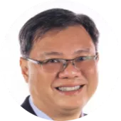
Meet the Speakers
Guest Speaker

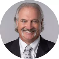
Ankur Srivastava
Director of the Institute for Systems Research
University of Maryland
Biography
Moderator

Warren Savage
Researcher at University of Maryland
Applied Research Laboratory for Intelligence and Security
Biography
United States
APHI ESD Alliance SiPATThe ESD Alliance, a SEMI Technology Community, is hosting a webinar series, "Savage on Security," moderated by Warren Savage, Researcher at University of Maryland, Applied Research Laboratory for Intelligence and Security.
Off Add to Calendar Disabled Register Now to Watch the Recorded EventHeterogeneous Integration (HI) has come a long way in 50 years. The world of multi-chip modules (MCMs) has given way to a vast ecosystem of chiplets, 3D stacked die, and co-packaging of antenna, high-bandwidth memory (HBM), and optics. HI is at the center of “More than Moore” development activities, as innovative engineers look for creative ways to overcome the slower scaling of silicon technology. The promise of HI is new devices with superior power, performance, area, and cost (PPAC). All these promises come with new challenges. Managing different process nodes, physical characteristics, mechanical stresses, and other system-level challenges not found in monolithic system-on-chip (SoC) devices, creates a great opportunity for design and manufacturing companies to reshape our industry.
In this webinar, we’ll explore this enabling technology from both the device maker and material supplier perspectives. We will learn about demands placed on devices by new applications and what new tools are needed to meet these demands. We will also hear about the challenges placed on materials and equipment suppliers to develop processes capable of manufacturing the individual components and integrating them into final products. Join us as our panel of experts address the issues and opportunities involved with heterogeneous integration.
United States
2nd Generation 3D V-Cache™ Enablement
Enabling Heterogeneous Integration through Material Design
The realization of Heterogeneous Integration (HI) has been key in driving advancements in semiconductor technology. The complexities of integrating dissimilar materials continue to be a challenge for HI. All advanced packaging technologies rely on advanced materials to address the many challenges in achieving continued shrinking and improved performance of devices. Novel materials capable of managing mechanical stresses and increased thermal budgets with strict cleanliness requirements are required for processes such as wafer thinning, fan-out wafer-level packaging, and hybrid bonding. This presentation will highlight how advanced materials can address the growing challenges in the industry.
Webinar Moderator
Dive into the dynamic world of semiconductor materials and discover the future landscape as the industry experts provide a glimpse into the future of the semiconductor ecosystem in the era of heterogenous integration.
INAUGURAL EVENT FOCUSED ON SMART MANUFACTURING & SMART MOBILITY
Join us for a groundbreaking Midwest conference and tradeshow on April 1-2, 2025, focused on Smart Manufacturing and Smart Mobility with an emphasis on the semiconductor industry! Automotive electronics and smart manufacturing are two of the key end markets on the path to $1T in semiconductor revenue.
A significant amount of both markets is concentrated in the Midwestern United States. SEMIEXPO in the Heartland will bring these two key markets together and provide an opportunity for collaboration and growth.
Smart Manufacturing
- The program will focus on the deployment of Industry 4.0 or Smart Manufacturing tools, technologies, and methods for the semiconductors required for this growing market.
Smart Mobility
- The program will unite stakeholders in the semiconductors/sensors and mobility ecosystems to identify and address technical issues and supply chain dynamics that are best addressed collectively.
Ways to Participate
- Exhibit
- Sponsor
- Speak
- Attend
MAKE YOUR MARK AT THE INAUGURAL SEMIEXPO HEARTLAND
Plan Now to Exhibit or Sponsor. Contact—
Shane Poblete | +1 202-847-5983 | [email protected]
STAY INFORMED: SEMIEXPO HEARTLAND—SEH Interest Form
Indiana Convention Center
100 S Capitol Ave
Detroit, MI
United States
Samsung Electronics Campus
3655 N First Street
San Jose, CA 95134
United States
The Heterogeneous Integration Roadmap activities are sponsored by IEEE Electronics Packaging Society (EPS), SEMI, IEEE Electron Devices Society (EDS), IEEE Photonics Society and the ASME EPPD Division with the intention of expanding the roadmap collaboration to other IEEE Technical Societies that share interest in the Heterogeneous Technology Roadmap as well as to organizations outside IEEE that share this common vision for the roadmap. A document with definition of the mission, purpose, structure and governance for this Heterogeneous Integration Roadmap program was prepared and approved.
1:00 pm - 5:00 pm Off Add to Calendar 2024-02-21 13:00:00 2024-02-23 17:00:00 Heterogeneous Integration Roadmap Symposium The Heterogeneous Integration Roadmap activities are sponsored by IEEE Electronics Packaging Society (EPS), SEMI, IEEE Electron Devices Society (EDS), IEEE Photonics Society and the ASME EPPD Division with the intention of expanding the roadmap collaboration to other IEEE Technical Societies that share interest in the Heterogeneous Technology Roadmap as well as to organizations outside IEEE that share this common vision for the roadmap. A document with definition of the mission, purpose, structure and governance for this Heterogeneous Integration Roadmap program was prepared and approved. Samsung Electronics Campus 3655 N First Street San Jose, CA 95134 United States SEMI.org [email protected] America/Los_Angeles publicSupporting Partners
This course will cover:
- Evolution of IC Packaging – Fan-in, Fan-out WLP, Embedded Packaging technology, System on Chip (SOC), System in Package (SiP), 3D IC, WLP, TSV etc.
- Principles of Interconnects ranging from TAB, Wirebond to various Flip Chip bonding such as thermocompression bonding with NCP, C4, ACF for manufacturing and R&D development
- Board level assembly and its soldering materials and failure mechanisms for 2nd level interconnect
- Overview of interposer of lead frame, ceramic, flex to BT substrates for Microelectronics Packaging
- Assembly flow and new assembly techniques such as stealth dicing, compression molding, underfill molding etc., and its assembly materials for Microelectronics packaging
- Material characterization from bulk to interfaces for Microelectronics packaging
Why should I attend?
- Gain technical knowledge for industry professionals
- Enhance knowledge in manufacturing and R&D know-how in IC packaging
- Apply Key Technical Concepts in Problem Solving through Real Case Studies
- Networking opportunities with industry peers
Who should attend?
- Beneficial for directors, managers, process & equipment engineers, R&D engineers and Quality & Reliability engineers working in the areas of microelectronics packaging
- Useful for sale or application engineers who supply packaging materials and tools to the industry
BROWSE OUR PHOTO GALLERY
Royale Chulan Penang
No 1 & 2, Pengkalan Weld, Georgetown
10300 Penang
Pulau Pinang
Malaysia
Introduction to IC Packaging & Interconnects
Introduction to IC Packaging
• Functions of Packaging – Mechanical, Material, Electrical and Chemical
• Review of Packaging Trend – BGA, CSP, Fan-in & Fan-out WLP, 3D Packaging, SoC vs SiP etc
• Challenges in Assembly and Packaging
Interconnects
• Overview
• TAB Bonding
• Wirebonding – Ultrasonic, Thermocompression, Thermosonic mechanisms
• Flip Chip Bondings – Thermocompression, C4, Re-cap reflow, solid-state, ACF, Conductive paste bonding
Lunch
Board Assembly and Soldering & PCB and IC Carriers
Board Assembly and Soldering
• Through Hole & SMT – Stencil Print Process, Reflow Profile
• Solder Materials – Alloy, Flux, Solvents, self-alignment effect
• Pb Free Solder – Ternary phase diagram, SnAgCu
• Intermetallics and Growth – Diffusion mechanism, Arrhenius equation
• Testing and Reliability – Ball shear & pull failure strength and modes, Fatigue, Weibull distribution
PCB and IC Carriers
• PCB Technology – Material properties, PCB fabrication process, drilling, patterning, plating, solder resist, laminating
• IC Carriers – Design rule, Leadframe, LTCC, Flex and BT substrates
• Substrate Development
Q&A | Case Studies
End of Day 1
Assembly Process
• Thickness Reduction – Grinding, Lapping, Polishing, CMP
• Dicing/Singulation – Blade, Laser, Stealth dicing, Dicing after grind
• Die Attach – Eutectic bonding, DA materials, Collets
• Plasma – Argon, Oxygen plasma, Surface tension
• Encapsulation – Mold constitutes and properties, Transfer, Film and compression molding, Dam and fill
• Plating – Solder plating, NiPd finish, PPF
• Trim & Form – ESD, Lead formation, Spring back mechanism
Lunch
Material Characterization Techniques
• Introduction
• Bulk Material Characterization – Stress strain, Bending, Impact toughness, TGA, DSC, TMA, DMA
• Interfaces Characterization – Failure mode and strength, Wire pull, Ball pull, Double cantilever bending, Die shear, Mold button shear, Ball shear
Q&A | Case Studies
Lucky Draw
End of Workshop
Note: Program is subject to changes.
Seminar 1 and Seminar 2 timing will overlap on 7 Mar .
Advanced Packaging and Material Characterization
*Note: Seminar 1 and Seminar 2 timing will overlap on 7 Mar
Participating Fee:
Usual Member Rate: SGD 750
Usual Non-member Rate: SGD 935
*The above rates are inclusive of coffee/tea breaks and luncheon for both days
Register before 23 February 2024 to enjoy Early Bird rate of 15% off the above rates.
A certificate of completion will be awarded at the end of the seminar.

*Malaysian Companies - HRDC Claimable for Penang Business Summit Seminar 1: Advanced Packaging (Advanced Packaging and Material Characterization) (subject to T&C, please contact HRDC for more information).
For HRDC claims, please refer to the following links on the claiming matrix and guidelines:
- HRDC Approval Letter for Penang Business Summit
- Allowable Cost Matrix
- HRDC SBL Grant Helper
- HRDC SBL Claim Helper
Contact us for enquiries!
For Program:
Ms. Cecelia Fong | [email protected] | +65.9750.2382
For Registration / HRDC Claims:
Ms. Gillian Lim | [email protected] | +65.9048.1123
Off Add to Calendar 2024-03-06 00:00:00 2024-03-07 00:00:00 Penang Business Summit Seminar 1: Advanced Packaging Advanced Packaging and Material Characterization*Note: Seminar 1 and Seminar 2 timing will overlap on 7 Mar Participating Fee:Usual Member Rate: SGD 750 Usual Non-member Rate: SGD 935 *The above rates are inclusive of coffee/tea breaks and luncheon for both daysRegister before 23 February 2024 to enjoy Early Bird rate of 15% off the above rates. A certificate of completion will be awarded at the end of the seminar. *Malaysian Companies - HRDC Claimable for Penang Business Summit Seminar 1: Advanced Packaging (Advanced Packaging and Material Characterization) (subject to T&C, please contact HRDC for more information).For HRDC claims, please refer to the following links on the claiming matrix and guidelines:HRDC Approval Letter for Penang Business SummitAllowable Cost MatrixHRDC SBL Grant HelperHRDC SBL Claim Helper Contact us for enquiries!For Program: Ms. Cecelia Fong | [email protected] | +65.9750.2382 For Registration / HRDC Claims: Ms. Gillian Lim | [email protected] | +65.9048.1123 Royale Chulan Penang No 1 & 2, Pengkalan Weld, Georgetown 10300 Penang Pulau Pinang Malaysia SEMI.org [email protected] Asia/Kuala_Lumpur public Asia/Kuala_Lumpur SOLD OUT
REGISTRATION
- Early-bird Registration Close: 5 pm, Tuesday, August 29(KST)
Registration Fee
- Pre-Registration (Until August 29)
| Price | SEMI Members | Non Members |
| 1 Session | KRW 120,000 | KRW 150,000 |
| 2 Sessions | KRW 200,000 | KRW 240,000 |
- On Site
| Price | SEMI Members | Non Members |
| 1 Session | KRW 150,000 | KRW 180,000 |
| 2 Sessions | KRW 240,000 | KRW 290,000 |
OVERVIEW
- Date: September 5(Tue), 2023
- Time: 09:00 – 17:30
- Venue: Hall 3, Suwon Convention Center
- Language: Korean / English (Simultaneous interpretation will be provided)
- Organizer: SEMI
SPONSORS
![]() | ![]() | ![]() | ![]() |
![]() | ![]() |
NOTICE
- The agenda will be subject to change without notice.
- Presentation files agreed by speakers will be provided to attendees.
CONTACT
- SEMI Korea Program Team ([email protected])
Suwon Convention Center
South Korea
Session 1: High-Performance Computing
Hetero Integration, High Performance Computing and AI
Xin Wu received PhD and MSc from University of California Berkeley USA and Peking University, China, respectively. Since 1993, he has worked in Xilinx (acquired by AMD in 2022) from 0.6um till 2nm generations of technologies and products, from many foundries and suppliers. His responsibilities include silicon, hetero-integration, advanced packaging, thermal mechanical solutions and many other technologies development.
PKG Interconnection Technology for HBM
Mr. Moon is currently working as a technical leader (VP) for package technology development, in SK hynix. He has more than 25 years’ experience in semiconductor package development including wafer level, flip chip and 2.5D/ 3D packaging as well as conventional package.
He previously served as package development project manager for package material, process and equipment until assuming his current role in 2022. And he has been involved in the development and mass production of NAND Flash, DRAM/ Mobile, MCP, RDL, Flip chip, WLCSP and TSV.
He received degree in chemistry from Sogang University in Seoul, Korea.
The next wave of Semiconductor Innovation – Multi-die system solution
Donghan Kim is a leader of Strategy Collaboration Solution Development at Synopsys Korea. He is responsible for leading 2.5D and 3D multi-die system solution business aiming to offer a complete end-to-end solution for efficient multi-die system integration.
He has more than 20 years of experience in semiconductor industry and has worked extensively on SOC mobile chip designs such as Exynos series at Samsung Electronics. He had a strong track record of successfully developing modem, WiFi and Bluetooth chipset products.
He received MS degree in electronic engineering from Sogang university in Seoul Korea where he did research topics on wireless communications and Semiconductor.
Status of High-End Performance Packaging (2.5D & 3D) - Technology and Market Trends
Stefan Chitoraga is a Technology and Market Analyst specializing in Packaging and Assembly at Yole Intelligence, part of Yole Group. Within the Semiconductor, Memory & Computing division at Yole, Stefan is focused on advanced packaging platforms and processes, substrates, and PCBs. He is involved daily in the production of technology & market reports and custom consulting projects.
Prior to Yole, Stefan served as a Package Design Engineer at Teledyne E2V for 4 years, where he was in charge of the ceramic package and glass lid development for image sensors, developing mechanical design, routing, electrical and thermal simulations.
Stefan holds a Bachelor’s in Electronics and Computer Science for Industry Applications from the Polytech Grenoble (France).
Break
Panel Discussion
Session 2: Interconnection Technology for HPC
Advanced Heterogeneous Integration
Jongsoo Choi, Ph.D. was appointed as head of marketing strategy part at Business Development Team of AVP Business, Samsung Electronics in December 2022, after completing Advanced PKG Task Force for six months. Before his new role, Dr. Choi was responsible for SoC product marketing as a director at System LSI Business from 2014.
Prior to joining the System LSI, Dr. Choi was Principal Engineer, and has led 4G mobile communication standards project at DMC R&D Center (now Samsung Research) since he joined Samsung Electronics in 2005, where he contributed to the 3rd Generation Partnership Project (3GPP) specifications which cover cellular telecommunications technologies, and also served as a vice chairman of 3GPP TSG GERAN from 2007 to 2011.
Dr. Choi received a Ph.D. degree in Electrical Engineering from the University of Ottawa, Ontario, Canada, where he focused research topics on wireless communications and adaptive signal processing.
Interconnect via scaling and challenges with hybrid bonding
Dr. Vikas Dubey, is a senior scientist at Fraunhofer ENAS since 2021 with system packaging department. He is into advanced system packaging for more than 10 years. He is currently leading the research activities related to hybrid bonding, collective die to wafer bonding and several other wafer bonding technologies for MEMS/NEMS integration. Besides, in his current role he is directly responsible for project acquisition, managing public and industrial projects and related to advance system integration, hybrid wafer bonding and assembly.
Prior to joining Fraunhofer ENAS he worked as a technology manager at national nanofabrication center (NNFC) at Indian Institute of Sciences, Bangalore. During his time at APTIV services located in hungary, he was responsible for several six sigma projects which lead to million of euros in earnings.
Dr. Dubey received his PhD degree from materials engineering department from KU Leuven, where he worked at imec with his research focused on self-aligned assembly for fine pitch integration.
Novel Materials for Advanced Packaging
Dongshun Bai, Ph.D. has been with Brewer Science, Inc. since 2007. Dongshun works as the Senior Technologist & Business Development Director in the Packaging Solutions Business Unit, in charge of technology roadmap direction of new material development for advanced packaging. He also leads the Business Development team and oversees the global business activities for advanced packaging materials.
Dongshun spent his first 10 years at Brewer Science in its Advanced Technologies R&D group. Working as Senior Program Manager and Senior Scientist, he led an R&D team focused on material design and development for advanced packaging. Many materials developed by his team went to commercialization and became the major products in the portfolio.
Dongshun earned a Ph.D. degree in Chemical Engineering from Vanderbilt University, Nashville, TN, USA and a Master of Engineering degree in Chemical Engineering from the National University of Singapore. Dongshun has published numerous papers and patents and delivered many talks, including invited talks at international conferences. He currently serves as a technical committee member for IMAPS and EPTC.
Laser Assisted Bond (LAB) Technology Overview
SeokHo Na joined Amkor Technology Korea in 1996 and worked for R&D engineer until now with responsibility of semiconductor material & process development. Major work is chip to substrate interconnection technology development such as wire bonding, Material Characterization, Flip Chip package CIP (chip to package interaction) and LAB (Laser Assisted Bonding) technology.
Prior to joining Amkor Technology Korea, Na received a bachelor’s degree and master’s’ degree in Material Science & Technology from Yeungnam University, Korea
Break
Panel Discussion
The Advanced Packaging Summit is a conference dedicated to exploring the latest advancements in packaging technology for high-performance computing (HPC) and interconnection. The summit brings together leading experts, researchers, and industry professionals to share their insights and experiences on advanced packaging solutions that enable high-density, high-bandwidth, and low-latency interconnects for HPC systems. Topics covered at the summit include 3D packaging, hybrid bonding, LAB(Laser Assisted Bonding), heterogeneous integration, supply chain management, and more. Attendees will gain valuable insights and have the opportunity to network with experts in the industry.
9:00 am - 5:30 pm Off Add to Calendar 2023-09-05 09:00:00 2023-09-05 17:30:00 Advanced Packaging Summit 2023 The Advanced Packaging Summit is a conference dedicated to exploring the latest advancements in packaging technology for high-performance computing (HPC) and interconnection. The summit brings together leading experts, researchers, and industry professionals to share their insights and experiences on advanced packaging solutions that enable high-density, high-bandwidth, and low-latency interconnects for HPC systems. Topics covered at the summit include 3D packaging, hybrid bonding, LAB(Laser Assisted Bonding), heterogeneous integration, supply chain management, and more. Attendees will gain valuable insights and have the opportunity to network with experts in the industry. Suwon Convention Center South Korea SEMI.org [email protected] Asia/Seoul public Asia/Seoul DISCOVER APS 2025