downloadGroupGroupnoun_press release_995423_000000 copyGroupnoun_Feed_96767_000000Group 19noun_pictures_1817522_000000Member company iconResource item iconStore item iconGroup 19Group 19noun_Photo_2085192_000000 Copynoun_presentation_2096081_000000Group 19Group Copy 7noun_webinar_692730_000000Path
Skip to main content
Default Banner Image

Business and Markets

The semiconductor industry faces an unprecedented paradox: AI demand is booming, fab investments are rising, yet wafer shipments remain stubbornly flat. What's driving this disconnect, and when will it break?As of mid-2025, the global silicon wafer market appears calm on the surface, but underlying structural tensions are quietly mounting. The demand for AI semiconductors remains resilient, and certain high-value supply chains continue to operate near capacity. Yet wafer shipments have shown little sign of meaningful recovery—a divergence that raises questions about the conventional supply-demand playbook.SEMI's latest Silicon Wafer Market Monitor Report begins with a structural hypothesis: that the current market dynamics cannot be explained solely by weak demand or delayed orders. Instead, we propose that the demand pattern of fab operations itself has fundamentally changed.The Hidden Constraint: Time ExtensionOne critical metric has emerged as a structural bottleneck—fab cycle time, or the average duration for a wafer to complete its full process flow. Our quantitative analysis reveals that since 2020, fab cycle times have grown at a compound annual growth rate of 14.8%. This represents a fundamental deceleration in fab throughput, meaning that even with the same number of tools and consistent utilization rates, the volume of wafers that can be processed is now structurally constrained.Why is this happening? Rising process complexity, increased equipment density, and tighter quality control requirements are absorbing more capital per wafer while paradoxically slowing production. Equipment spending per wafer area has surged over 150% since 2020, yet this investment translates into longer processing times rather than higher throughput.The High Bandwidth Memory (HBM) Economic ThresholdSimultaneously, the market is approaching a new inflection point driven by the rapid rise of HBM. HBM wafers consume over three times more wafer area per bit compared to standard DRAM, creating potentially significant wafer demand. However, HBM currently accounts for just 16% of total memory revenue—still below a critical economic threshold.Our analysis identifies that when HBM reaches 25% of total memory revenue, the trade ratio rises to 1.5. This is the structural breakeven point where CapEx per wafer for HBM-dedicated lines aligns with standard DRAM economics. At this threshold, memory makers gain clear incentives to expand wafer input, and customers become more willing to pay premium prices.The Quantitative FrameworkInstead of relying on conventional forecasts, we model the interaction of four critical variables—HBM penetration, DRAM bit growth, fab utilization, and cycle time—using a quantitative simulation framework. Under current conditions (16% HBM revenue share, 15% annual bit growth, 95% fab utilization, and 14.8% cycle time increase), wafer input would need to increase by 23.9% annually to meet projected demand.Yet no fab is scaling wafer input to that extent today. This suggests the market isn't demand-constrained but operating within a conditionally responsive system—one that won't activate until key thresholds align.Beyond Economics: Technical and Operational ReadinessThe slow pace of HBM expansion isn't solely about investment timing. Technical constraints including low yields, delayed customer qualification, and process stabilization challenges also play critical roles. These preconditions—investment readiness, yield optimization, and qualification completion—haven't yet aligned, keeping the market in strategic latency despite robust underlying demand.Additional factors compound this delay. Backend bottlenecks in Chip-on-Wafer-on-Substrate (CoWoS) packaging are causing semi-finished wafers to accumulate as inventory, constraining upstream wafer input. At the fab level, companies prioritize efficiency gains through process conversions over new construction. Meanwhile, macroeconomic uncertainty, geopolitical tensions, and foreign exchange volatility continue suppressing capital execution.The Three-Tier Response ModelThis structural shift creates a three-tier demand response across the supply chain:Wafer demand: Conditionally responsive, awaiting economic threshold alignmentEquipment investment: Process-transition driven, already responding to complexity increasesMaterials demand: Directly tied to cycle time extensions, with potential for early bottlenecksFor certain process-critical materials like EUV photoresists and TSV chemicals, supply constraints may emerge even before wafer input fully ramps, preceding equipment expansion.Strategic ImplicationsFor industry stakeholders, this analysis suggests three key actions: wafer suppliers should prepare scenario-based capacity plans around the 25% HBM threshold; equipment makers should anticipate process-transition driven demand regardless of current wafer volumes; and materials suppliers should prepare for potential bottlenecks as extended cycle times increase consumption per wafer.Crucially, the current stagnation shouldn't be interpreted as structural decline. Rather, the market exists in a state of strategic readiness, with key conditions not yet aligned. Once they are, wafer demand will likely respond nonlinearly—and momentum is already building in that direction.The structural inflection point (≈25% HBM penetration) and cycle time increase (+14.8%) serve as forward-looking indicators not just for wafer producers, but for the entire upstream supply chain. The question isn't whether this inflection will occur, but when. Companies that understand these structural dynamics and prepare accordingly will be best positioned to capitalize on the nonlinear demand response when it arrives.These key insights are from the market update section of the Q2 2025 Silicon Wafer Market Monitor Report. This quarter's analysis models structural inflection points using scenario-based projections across nine core charts and tables, offering data-driven perspective on the industry's readiness for the next demand shift. Download your free sample report today.For more information on the report or to subscribe, please contact the SEMI Market Intelligence Team at [email protected]. Details on the complete SEMI market data portfolio are available at our Market Intelligence website. Sungho Yoon is a Principal Analyst in the Silicon Wafer Market Research at SEMI Market Intelligence.
Read More
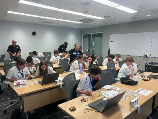
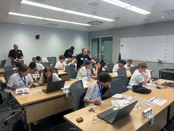
The semiconductor industry is grappling with a critical talent shortage, both globally and within the United States. At the same time, the workplace landscape for high school and college graduates is changing. These dual pressures present an opportunity: to cultivate early career awareness by introducing K–12 students to dynamic, real-world learning experiences that open their eyes to emerging industries—like semiconductors—and the meaningful roles they could play in them.Investing in this early exposure strengthens the long-term talent pipeline for the semiconductor industry and prepares students to meet the demands of a rapidly evolving workforce. However, realizing this vision requires intentional, cross-sector collaboration among educators, industry leaders, workforce boards, and policymakers.One example of this type of collaboration is the ChipWorks Series in Idaho. Boise State University partnered with Micron, the Idaho Workforce Development Council, and the Idaho Digital Learning Alliance to design, develop, and launch the learning experience for middle and high school students in 2024. The ChipWorks Series consists of three courses: Chip, Chip, Hooray!; Introduction to Electrical and Computer Engineering; and Materials Science and Engineering. With the first course launching in Fall 2024, the program has already reached over 220 learners across Idaho – and it’s just getting started. Camille Platts-McPharlin is the Project Manager at the Microelectronics Education and Research Center helping Boise State prepare to expand their programming to a national audience in 2025.The origin of the ChipWorks Series began through a grant with the Idaho Workforce Development Council. “The Council and Boise State University saw an opportunity to address the growing workforce gap by building a pipeline that begins in middle school and goes through adulthood,” said Platts-McPharlin. Development began in 2023 and was shaped by more than 300 voices from industry, academia, and K–12 education. This cross-sector group of stakeholders worked collaboratively to ensure that the lessons were responsive to real-world industry needs and compatible with classroom delivery best practices. Furthermore, the courses are aligned with State and National learning standards as well as ABET standards. Overcoming logistics challenges around open-source resources and existing structures in formal education led to two of the programs being dual credit, setting high school students up for early success in post-secondary. There has been an enthusiastic response from learners across Idaho, and more learners are expected to engage this year, as the third and final course is launched in the fall. Students enroll at their home school, have the support of local teachers, and receive online instruction synchronously from a dedicated teacher through the Idaho Digital Learning Alliance. This model enables a broader group of learners to access the training, regardless of educator understanding of the content. Students learning ChipWorks Series lessons at Micron Chip Camp.The ChipWorks Series is now expanding its reach beyond Idaho. In collaboration with Micron, Platts-McPharlin and the MERC team are working to bring the courses to students in New York. Educators from Syracuse and surrounding districts participated in a week-long professional development event to learn the curriculum and begin the work of bringing it into their local school districts. Teacher training for educators from Idaho and New York. Platts-McPharlin offered words of wisdom for other educators, training providers, or partners who are trying to create industry awareness opportunities earlier in the learning journey. “The key to success is listening closely to stakeholders and balancing the various perspectives. This will result in a quality product,” she said. Her other suggestion: trust the process. While it was challenging to build entirely new programs, the impact it is having on students, their teachers and their families to make them aware of their potential is immense. Programs like ChipWorks offer a powerful solution to the semiconductor industry’s workforce crisis, but they cannot stand alone. For sustained progress, industry leaders, workforce development councils, and educational institutions must work together to co-design scalable, inclusive solutions. This means sharing expertise, investing in infrastructure, and championing long-term talent development—starting in the earliest years of education. For more information on the ChipWorks Series, or to learn how to bring it to your students, please contact Camille Platts-McPharlin: [email protected]. To learn about what the SEMI Foundation is doing to bring together cross-sectoral groups for similar projects, contact Anissa Hamdon-Morison: [email protected] Hamdon-Morison is Training and Curriculum Manager at SEMI Foundation.
Read More
“Critical minerals our world needs for electric vehicles and semiconductors can be found here. Clean energy we need to power artificial intelligence data centers and economic growth can be built here.”[1] This statement was made by former US President Joseph Biden during his visit to Angola in December 2024 to support a US-funded railroad project called the Lobito Corridor. The railroad would connect mining areas in the Democratic Republic of Congo (DRC) and Zambia to a port on the western coast of Africa, an important step towards expanding access to critical minerals needed for growth of the semiconductor and energy industry in the west. According to the Intergovernmental Forum on Mining, Minerals, Metals and Sustainable Development (IGF), “there is no universally agreed upon definition of what ‘criticality’ means…criticality is also very country- and context-specific, particularly with respect to mineral endowment, the relative importance of the minerals to industrial and economic development, and a strategic assessment of supply risks and volatility.”[2] In other words, the term “critical mineral” may vary by location, application, and current events. Many countries have generated their own lists of critical minerals to help guide legislation, budgetary allocations and diplomatic efforts. For example, the United States Geological Survey released a list of “50 mineral commodities critical to the US economy and national security” in 2022 which included 10 minerals that were directly linked to semiconductors and electronics.[3] These included arsenic, dysprosium, gallium, lutetium, rhodium, ruthenium, tantalum, terbium, tin, and tungsten. Other lists might include cobalt, copper, and sometimes uranium. For most countries that make chips and electronics, critical minerals are both essential for supporting their industry and also hard to find within their own borders.While downstream electronics and semiconductor manufacturers are often located in countries with robust labor protections, the extraction of raw minerals too often takes place under less humane circumstances. In April 2024, the UN Secretary General launched the Panel on Critical Energy Transition Minerals to address the challenges associated with responsible extraction of critical minerals. One of the motivations for the formation of the panel was the concern about human rights violations related to mineral extraction. “Mining, at all scales, large and small, has too often been linked with human rights abuses, environmental degradation and conflict.”[4] The term “conflict mineral” has a much narrower definition than critical mineral, and usually only refers to tin, tantalum, tungsten and gold, also known as ‘3TG’. This definition is often used in policy frameworks, such as the US Dodd-Frank 1502 Act[5] and the European Union (EU) Regulation 2017/821[6]. These four minerals were identified as a major source of income for armed groups in the DRC, fueling a decades long war that has claimed more than 6 million lives since the start of the Second Congo War in 1996.[7] For example, in May 2024, armed groups from Rwanda captured a town in the Congo with the largest coltan mine in the country, which is the second largest producer in the world of the ore that is refined to make tantalum - a key component of capacitors. The incursion helped to finance the armed group, collecting at least $800,000 per month in taxes.[8] Over the past 15 years, several frameworks have emerged to address the conflicts and tensions stemming from extraction of critical minerals. A common framework within the semiconductor industry was written by the Organization for Cooperation and Development (OECD), which is an intergovernmental economic organization founded in 1948 (then known as OEEC) to “build better policies for better lives.” The organization publishes several guidelines, including the OECD Due Diligence Guidance for Responsible Business Conduct[9] (see suggested measures in Figure 1) and the OECD Due Diligence Guidance for Responsible Supply Chains of Minerals from Conflict-Affected and High-Risk Areas with focuses specifically on 3TG minerals.[10] These guidelines provide a structure through which companies and organizations might address human rights and environmental issues that may arise from their or their suppliers’ operations. Figure 1: Due Diligence Process and Supporting Measures from the OECD Due Diligence Guidance for Responsible Business Conduct (2018)Several regulations have been implemented by governing bodies to prevent financing of armed groups through procurement of conflict minerals. In the United States, Section 1502 of the Dodd-Frank Wall Street Reform and Consumer Protection Act requires certain companies to “publicly disclose their use of conflict minerals that originated in the Democratic Republic of the Congo or an adjoining country.”[11] Also known as the “Disclosure Rule,” a company must file a report to the Securities and Exchange Commission (SEC) describing the source and chain of custody of its conflict minerals, and must also conform to a nationally or internationally recognized due diligence standard such as the OECD guidelines. Similarly, the EU Regulation 2017/821 refers to the OECD Due Diligence Guidelines and calls on companies within the EU to monitor, audit and disclose procurement of conflict minerals. In 2024, the EU furthered its efforts to address human rights and environmental issues by adopting the EU Corporate Sustainability Due Diligence Directive (EU CSDDD). This directive will require all companies that do business within the EU, regardless of country of origin, to monitor their supply chains for labor and environmental violations or risk penalty.Given the tremendous effort by the industry to address the conflict associated with 3TG minerals, it is unclear whether these efforts have had an effect. The U.S. Government Accountability Office (GAO), which serves as the federal government’s watchdog agency and is tasked with providing Congress with independent, nonpartisan information, has been reporting on issues related to conflict minerals in the DRC since 2010. Kimberly Gianopoulos, Managing Director of GAO’s International Affairs and Trade Team, has led this body of work over time, including GAO’s most recent report, which was published in October 2024. Gianopoulos stated that, “although it has been over a decade since the SEC issued its conflict minerals disclosure rule in 2012, GAO’s most recent report found that there is no empirical evidence that the rule has decreased violence in the eastern DRC, where many mines and armed groups are located, and that a majority of companies that conduct due diligence on their mineral supply chains continue to report being unable to determine the origins of minerals used in their products.” The 2024 Conflict Minerals report can be found here: https://www.gao.gov/products/gao-25-107018.Regulatory approaches are only one way in which the semiconductor industry interacts with conflict mineral issues. Many companies and industry associations have implemented their own initiatives and formed associations to share resources to trace materials and collect supplier information. One such industry association is the Responsible Business Alliance’s Responsible Minerals Initiative (RMI). Jennifer Peyser, the executive director of the RMI, stated that the initiative “supports over 500 downstream, midstream, and upstream member companies with a suite of due diligence standards and tools, data, guidance, training, and other resources for global responsible sourcing and regulatory compliance. Our facility and supply chain due diligence standards are rooted in longstanding international norms while reflecting emerging corporate and stakeholder priorities for regulatory compliance, managing sustainability risks and impacts, and fostering responsible mineral supply chains.” More information about the RMI can be found here: www.responsiblemineralsinitiative.org.Recently, SEMI has formed a new Responsible Supply Chain (RSC) working group under its Supply Chain Management initiative to provide a platform for enabling traceability and provenance across the supply chain to meet government regulations on conflict minerals and unfair labor practices. This new working group aims to bring together SEMI member companies to raise awareness of key issues, share resources, and advocate effective regulations and standards. The working group is comprised of SEMI member company employees from a wide range of backgrounds, including sustainability managers, supply chain experts and process engineers. If you are interested in joining our discussions, please visit our website for more information: https://semi.huihuidehui.workers.dev/en/industry-groups/supply-chain-management. On July 9 at 8am Pacific/11am Eastern, the SEMI Responsible Supply Chain working group will host a webinar featuring a roundtable discussion with Jennifer Peyser, Executive Director of the Responsible Business Alliance’s Responsible Minerals Initiative, and Kimberly Gianopoulos, Managing Director of the International Affairs and Trade Team at the US Government Accountability Office, including Q A for attendees to join the discussion. Visit https://semi.huihuidehui.workers.dev/en/event/critical-minerals-due-diligence-and-semiconductor-supply-chain to register.Other upcoming events include a panel discussion at SEMICON West, October 7-9, 2025 in Phoenix, Arizona!Author Bio:Dr. Kimberly Harrison Ph.D is a Senior MEMS Designer with AMFitzgerald Associates, a design firm located in the Bay Area California. She has a doctoral degree in mechanical engineering from Stanford University, and has worked as a designer and process engineer in the semiconductor industry for 10 years. She was nominated as a 2022 MEMS Sensors Industry Group Emerging Leader. As a founding member and leader of the SEMI Responsible Supply Chain Working Group, she hopes to bring SEMI members together to discuss solutions to human rights issues in the semiconductor supply chain.References:[1] Remarks by President Biden Participating in the Lobito Corridor Trans-Africa Summit in Benguela, Angola (December 4, 2024). https://bidenwhitehouse.archives.gov/briefing-room/speeches-remarks/2024/12/04/remarks-by-president-biden-participating-in-the-lobito-corridor-trans-africa-summit-benguela-angola/[2] Critical Minerals: A Primer (November 1, 2022). https://www.igfmining.org/resource/critical-minerals-primer/[3] https://www.usgs.gov/news/national-news-release/us-geological-survey-releases-2022-list-critical-minerals[4] Resourcing the Energy Transition: Principles to Guide Critical Energy Transition Minerals Towards Equity and Justice (April 11, 2024). https://www.un.org/en/climatechange/critical-minerals[5] https://www.sec.gov/resources-small-businesses/small-business-compliance-guides/conflict-minerals-disclosure[6] https://eur-lex.europa.eu/eli/reg/2017/821/oj/eng[7] Conflict in the Democratic Republic of Congo (March 20, 2025). https://www.cfr.org/global-conflict-tracker/conflict/violence-democratic-republic-congo[8] The Evidence that Shows Rwanda is Backing Rebels in DR Congo (January 29, 2025) https://www.bbc.com/news/articles/ckgyzl1mlkvo[9] OECD Due Diligence Guidance for Responsible Business Conduct (February 1, 2018). https://www.oecd.org/en/publications/oecd-due-diligence-guidance-for-responsible-business-conduct_15f5f4b3-en.html[10] OECD Due Diligence Guidance for Responsible Supply Chains of Minerals from Conflict-Affected and High-Risk Areas, 3rd edition (April 6, 2016). https://www.oecd.org/en/publications/oecd-due-diligence-guidance-for-responsible-supply-chains-of-minerals-from-conflict-affected-and-high-risk-areas_9789264252479-en.html[11] https://www.sec.gov/resources-small-businesses/small-business-compliance-guides/conflict-minerals-disclosure
Read More
Under the Greenhouse Gas Protocol (GHGP), all companies are required to calculate and report their emissions, including those of all members of their downstream and upstream supply chains. These are called Scope 3 emissions, and are divided into 15 Categories, including Category 11 - Use of Sold Products, a heavy lift for many small (and often large) companies. Measurement and improvements in vendor Scope 3 emissions are already influencing vendor selection and sourcing decisions, and experts agree that this will continue to increase. Upstream suppliers have typically relied on broad GHGP guidance to follow in making their calculations. For the semiconductor sector, and its well-documented, incredibly complex supply chain, there was no guidance accounting for the nuances within the industry to standardize calculations. Work began a year-and-a-half ago to change that.The Semiconductor Climate Consortium (SCC)’s Scope 3 Working Group compiled, verified and published a guidance document for calculating Scope 3, Category 11 emissions. The guidance document helps standardize emissions reporting and calculation methods and accounts for the unique requirements and circumstances of the semiconductor value chain.The SCC 3.11 guidance explicitly highlights where it maintains consistency with the existing guidance (e.g., GHG, SBTi, US EPA) and where it expands on that guidance to close a gap relevant to one or more of the semiconductor industry segments. The document was developed with the help of the Sustainability Consulting Group ERM, as well as excellent participation from the Scope 3 Working Group members, including representation from every segment of the semiconductor value chain from IDMs to foundries, fabless companies, chemical gas and materials companies, OSATS, and equipment manufacturers.Some of the significant areas considered while compiling the guidance included:Boundaries, especially around products and direct use-phase emissionsProduct lifespan, especially across the different sectors of the value chainMarket based emissions guidanceIncorporating grid decarbonization into the inventory and calculationsThe document includes several useful calculation examples, including direct use phase emissions and direct and indirect energy consumption. The examples help to make the guidance more tangible and practical in real world application.We were pleased to collaborate with our industry colleagues on developing this guidance as we work to align with others in the industry and minimize our reporting via efforts by the SCC. Download the Guidance Document.For further insights into the Guidance, the authors, including experts from ERM recently hosted a webinar. Register to watch the recording. Sara Turner is Climate Program Manager at Lam Research, and Mike Halblander is Product Marketing Manager at Teradyne. Both Turner and Halblander lead the SCC’s Scope 3 Working Group.
Read More
The SEMI Startups for Sustainable Semiconductors (S3) program, now in its 4th year of inviting startups to apply, is pleased to announce the 35 startups chosen to move to the semi-finalist virtual pitch event happening July 31 and August 1. From this pool, 10-12 finalists will be chosen and invited to pitch to a live audience at SEMICON West 2025 in Phoenix, AZ, October 7-9, 2025. The committee, made up of experienced Corporate Venture Capitalists (CVCs) from the global semiconductor industry, received impressive submissions in all three categories identified for 2025:Sustainable Semiconductor ManufacturingSustainable Data CenterGen AI for Sustainable DesignLed by Applied Materials this year, the program’s strongest feature is the exposure to the CVCs, as well as the personal mentoring each semi-finalist receives. The mentoring topics are tailor made to align with the greatest need of the startup and can range from basic introduction to semiconductor manufacturing, to connecting them to funding sources. A full analysis of the program kicked off this year’s efforts. The program saw a 100% increase in applications to 145 this year and thus the pool of semifinalists expanded from 30 to 35. While geographically diverse, the semi-finalists all share their solutions for the building and use of more sustainable electronics. Are you an investor and would like to receive notice of the virtual and live pitch events around S3? Register your interest here.2025 S3 Semifinalists3D Architech, Inc.Boston, MA, USA 3D Architech develops and commercializes advanced cooling devices for AI chips using a proprietary gel-based metal 3D printing technology. Unlike conventional methods limited to 100-micron structures, our technology enables highly complex microstructures at 10-micron precision, achieving up to 60% improvement in cooling efficiency. Actasys Inc.Brooklyn, NY, USAActasys has developed a precision cooling solution designed for thermal bottlenecks in semiconductor-driven systems such as networking cards (NICs), DPUs, switches, and optical transceivers. Instead of cooling entire racks or server rooms ActaJet™ targets localized hotspots at the device level, delivering scalable, high-efficiency airflow through a compact, adaptive, and electronically controlled actuator system. AlixLabs ABLund, SwedenAlixLabs AB is developing a disruptive semiconductor manufacturing technology based on Atomic Layer Pitch Splitting (APS). It enables cost-effective and environmentally sustainable scaling of transistor architectures by doubling pattern density without requiring advanced lithography. The core product includes both the APS process and customized etching equipment that integrates into existing semiconductor fab workflows, reducing complexity, cost, and environmental impact.AllonniaBoston, MA, USAAllonnia™ Surface Active Foam Fractionation (SAFF) unit is a turnkey PFAS remediation system engineered for on-site deployment. The system employs foam fractionation to physically separate PFAS from contaminated water streams, including both long- and short-chain compounds. SAFF arrives in a standard container and requires only electrical power, influent, and effluent hookups, and is telemetry-enabled for remote monitoring and control.Alloy EnterprisesBurlington, VT, USAAlloy Enterprises develops and manufactures cold plates, manifolds, and integrated thermal solutions for liquid cooling GPUs, CPUs, and other high-performance components in data centers and semiconductor equipment. Alloy utilizes a patented Stack Forging® process to enable direct-to-chip cooling to improve thermal performance and reduce pressure drop by up to 40 times, enabling data centers to run 44°C water and reduce pumping power.AlsemySeoul, South KoreaAlsemy is building an AI-powered platform that bridges Manufacturing Execution Systems (MES) and EDA domains enabling fabless engineers to reflect manufacturing data characteristics in their chip designs, while process engineers can make data-driven decisions to optimize manufacturing processes for maximum chip performance. By connecting these traditionally siloed areas, a feedback loop is created to drive efficiency and innovation across the semiconductor value chain.Arieca IncPittsburgh, PA, USAArieca's adaptable Liquid Metal Embedded Elastomer (LMEE) technology, which blends liquid metal and polymer, delivers both thermal performance and mechanical reliability. LMEEs are a cost-effective, dispensable emulsion that is compatible with existing high volume manufacturing tools and allows for low pressure spreading and excellent wetting. Atomos 3DWest Lafayette, IN, USAAtomos 3D offers low temperature transistor technology for monolithic 3D chip integrationCoflux Purification, IncHouston, TX, USACoflux Purification is developing a modular, point-of-use reactor system that both captures and destroys PFAS in semiconductor wastewater using our patent-pending Covalent Organic Frameworks (COFs). These materials serve as photocatalytic adsorbents, combining high surface area, tunable porosity, and chemical stability to enable efficient PFAS adsorption and UV-driven degradation within a compact, modular system ensuring smooth operational deployment. CoolSem TechnologiesEindhoven, The NetherlandsCoolSem is developing a breakthrough thermal management technology for semiconductor devices. The Wafer Level Thermal Interface Stack (WLTIS) enables 1) up to 15x better thermal management; 2) 25-55°C lower chip temperatures; 3) 2-4° increase in device performance, reliability, and lifespan; and 4) up to 30-50% reduction in cooling energy needs. CoolSem help handle the exploding demand for AI training and inference without proportional increases in power usage or carbon footprint.CuspAICambridge, UKCuspAI is building an engine that combines Gen AI models, virtual twins, and active learning pipelines for simulation to develop sustainable materials solutions that address critical environmental challenges, including, environmentally-friendly etching reagents, specialized sorbents for emissions capture, and novel catalysts for manufacturing waste remediation. The engine has already proven successful in designing metal-organic frameworks (MOFs) for carbon capture and PFAS removal from water.FlexiramicsEnshede, The NetherlandsFlexiramics® is a flexible, 100% ceramic fiber material engineered as a drop-in replacement for PCB substrates. It dramatically improves heat dissipation and signal integrity in high-performance electronics, enabling faster, cooler, and more reliable semiconductor systems.FluorityxWatertown, MA, USAFluorityx is commercializing a portable low-cost polymer sensor for PFAS. This fast and efficient system will be able to measure low concentrations of PFAS and replace expensive equipment and does not require highly trained staff to operate and maintain the equipment.Forever AnalyticalSouth Bend, IN, USAForever Analytical is developing a field-deployable sensor capable of providing real-time total fluorine (TF) mass-balance information. The company is also developing a mass-spectroscopy based solution that can be coupled with the sensor to provide information on the specific PFAS molecules present in the waste stream and can be adapted to measure other contamination of interest, such as heavy metals, lead, and copper.Gallox Semiconductors Inc.Ithaca, NY, USAGallox Semiconductors is dedicated to commercializing beta-gallium oxide (Ga2O3)-based transistors and diodes. Our patented device topologies take advantage of Ga2O3's large bandgap (~4.8 eV), which enables lower conduction losses and higher voltage handling compared to SiC. Higher voltage operation means greater power densities and system-level efficiency, effectively generating less waste heat and reducing both energy loss and cooling burdens.IC Recovery, a Division of Greene Lyon Group, Inc.Beverly, MA, USAIC Recovery's multi-patented CHIP-RENEW® technology uses a proprietary process to apply a unique thermal fluid to the surface of PCBs until the solder alloy attaching chips and other components to the board substrate reaches temperature liquidus. At that point, we can selectively recover functionally valuable chips for renewal and reuse, and/or harvest all other chips and components on the board in order to concentrate their content for subsequent, sustainable refining.icspiKitchener, ON, CanadaIcspi has created a complete atomic force microscope (AFM) scan head on a 1 mm x 1 mm chip - 1 million times smaller than traditional AFMs and the future of nanoscale semiconductor metrology and inspection powered by arrays of thousands of micro-AFM devices. The technology boosts wafer coverage and speeds time-to-yield and reduces scrap. Kelvin Cooling Inc.Berkeley, CA, USAKelvin Cooling introduces high-efficiency nano-film evaporation cooling technology - enhancing thermal management by increasing heat transfer efficiency while reducing power consumption. This thin-film evaporation system enables direct-to-chip cooling, in a compact, scalable, and energy-efficient platform.LinqueMunich, GermanyLinque provides an integrated photonic switch (IPS) enabling AI-capable network nodes with reconfigurable all-optical routing for high data-rate channels with ultra-low latencies suitable for scale-out and scale-up layers of data center networks.Makr MicrosystemsBangalore, IndiaMakr Microsystems has developed a novel approach to AcousticAtomic Force Microscope (AFM) that uses common AFM instrumentation and simplifies interpretation, with a modified probe geometry that enables both acoustic transduction and sensing. We have demonstrated nanometer scale imaging from samples with shallow and deep subsurface structures.MatnexLondon, UKMatnex platform uses AI to rapidly scan the periodic table, allows input of objectives (functional electronic, optical, or mechanical properties) and constraints (element exclusions, intrinsic price, emission limits, etc.), and then searches a proprietary database to identify suitable stable candidates and their production methods. This provides fit-for-purpose materials that reduce environmental impact, improve the bottom line, and open new markets with technological breakthroughs.Mixx Technologies, Inc.San Jose, CA, USAMixx Technologies is a deep-tech startup building next-generation optical interconnect solutions to deliver non-blocking, energy-efficient data movement. The advanced 3DS platform enables petabit level end-to-end connectivity for AI workloads resulting in sustainable, efficient, and cost-effective scaling. The 3DS platform comprised of the engine, package and system, enables seamless deployment of the optical IO chiplet.Nano Performance Technologies Ltd.Coquitlam, BC, CanadaNano Performance Technologies (NPT) is developing next-generation nanomaterials, specifically, Tellurene and Bismuthene (2D materials) and ultra-pure gold nanoparticle, for use in semiconductors, quantum computing, and advanced biosensing. The innovation is the scalable production and commercialization of these materials. The platform combines IP from Purdue University with in-house lab capabilities, enabling a supply of application-ready nanomaterials to R D and manufacturing partners.NextGO EpiBerlin, GermanyNextGo Epi delivers high-quality and large-scale Gallium Oxide epiwafer for high-voltage (up to 10kV-level) applications that are durable in high-temperature operations and environments with high radiation levels.NextoarBangalore, IndiaNextoar is a deeptech AI startup, focused on using AI to train the frontline fab technicians, equipment engineers, maintenance engineers, test engineers, service engineers, etc., and others closest to the action. The system will make them part of the innovation engine by, augmenting frontline workers, amplifying their business impact and creating continuously innovating organizations.PhysicsXNew York, NY, USAThe PhysicsX platform is an AI-driven simulation software stack designed to speed up traditional numerical simulations, optimizes components within defined constraints, and generate innovative geometries using generative Large Geometry Models (LGMs). The technology seamlessly integrates into enterprise engineering workflows, driving tangible improvements in product design, manufacturing, and operations and has several successful implementations in the electronics ecosystem.Point2 TechnologySan Jose, CA, USAPoint2 designs and manufactures mixed-signal interconnect SoCs for terabit data transmission, to overcome the barriers of copper and optical cabling to accelerate AI interconnect in GPU cluster scale-up. e-Tube technology uses an RF Transmitter SoC to convert data from the electrical to the RF domain for transmission over plastic waveguides, with the RF Receiver SoC converting the data from the RF domain back to the electrical domain.PROUDLausanne, SwitzerlandPROUD's patented diamond-layer technology with the highest heat dissipation capacity ( 1000 W/m.K) of any existing material, deposited on chips, allows a direct upgrade in heat extraction, power output and efficiency.Scrona AGZurich, AustriaScrona has developed a scalable multi-nozzle electrohydrodynamic (EHD) inkjet printhead for additive microfabrication in semiconductor and electronics manufacturing. This MEMS-based 128-nozzle printhead enables sub-10 nm resolution, ultra-low material use, and wide material compatibility, including metals, dielectrics, and polymers. It replaces wasteful lithography and etching with direct-write precision printing, significantly reducing energy, water, and chemical consumption in an automation-ready format.SKYRE, Inc.East Hartford, MA, USASKYRE develops and manufactures products for on-site purification and pressurization of process hydrogen and makes it available for reuse at the fab facility. The hardware is highly reliable with low maintenance costs with equal or better quality and lower cost than merchant hydrogen or onsite hydrogen generation.SyentaSydney, AustraliaSyenta has developed LEM - Localized Electrochemical Modelling - a process for depositing metal patterns using a local electrochemical process. The pattern is created on a stamp, which then prints the pattern on the substrate in an additive process.Terecircuits CorporationMountain View, CA, USATerecircuits develops advanced material solutions for heterogeneous assembly of small, fragile, and thinned components, Chiplets, sensors, power devices, and passives. The process is ideal for achieving scale with reduced waste; while meeting critical assembly challenges such as 3D assembly, silicon carbide die attach, flexible circuits, and optics. Vertical HorizonsCambridge, MA, USAVertical Horizons is a fabless semiconductor company commercializing vertical gallium nitride (GaN) power transistors to revolutionize energy efficiency. Vertical GaN reduces energy losses by up to 30% and doubles power density, enabling a 50% reduction in system footprint. This innovation tackles the urgent need for a new generation of power infrastructure designed to scale AI, and high-density and high-power applications.Vionano Innovations IncSt. Paul, MN, USAVioNano Innovations is building a patterning platform to enable advanced feature scaling using self-assembling polymer brush materials. The system enables polymers over 193 nm DUV lithography patterns to double feature density without requiring ALD/CVD or etch steps. The result is a low-energy, high-resolution process for sub-20 nm features using existing infrastructure.XLYNX MaterialsVictoria, BC, CanadaXLYNX designs and manufactures a revolutionary family of polymer crosslinkers. These reagents are uniquely able to cure virtually ANY aliphatic polymer, by harnessing high-yielding insertions to carbon-hydrogen bonds. Curing can be triggered thermally (at temperatures as low as 80°C) or photochemically (using either UV or blue light). Heidi Hoffman is Senior Director, Marketing Sustainability at SEMI.

Read More
The semiconductor industry faces an uncomfortable contradiction. Markets are expanding and demand continues rising, but the talent pool is shrinking.By 2030, the industry will need to add 1 million skilled workers globally, with shortages of over 100,000 engineers in Europe and more than 200,000 engineers in Asia-Pacific. This expansion requires at least 100,000 second-line leaders and 10,000 third-line leaders—many of whom must come from outside the industry.Markets Keep Growing, Leadership Doesn'tThe industry's outlook remains optimistic. Nearly one in five (19%) semiconductor executives anticipate continued demand growth without inventory excess in the next four years. Global sales hit $627.6 billion in 2024—a 19.1% increase driven by AI advancements, consumer electronics demand, 5G adoption, and automotive innovation.Governments are backing this growth with large investments too. The European Chips Act aims to double the EU's production share to 20% by 2030 with €43 billion. Companies like NXP Semiconductors, Infineon Technologies, and STMicroelectronics are expanding. Taiwan Semiconductor Manufacturing Company (TSMC) remains the world's largest contract chipmaker. The UK government unveiled a £1 billion strategy over 10 years, while the CHIPS and Science Act allocated $52.7 billion for US manufacturing and research.But there aren't enough semiconductor leaders to manage this growth.The Education CrisisThe talent shortage begins in universities. Electrical engineering and computer science enrollment has been declining for years. Germany saw 6.5% fewer STEM students in 2021 than the previous year.An analysis of recent data shows concerning patterns. While Germany had 81,934 electrical engineering students in 2018, Ireland had only 742 new electrical engineering students in 2017. The United States awarded just 13,767 bachelor's degrees in electrical engineering in 2018.Retirement and Skills GapsWhile universities produce fewer graduates, experienced leaders are retiring. One-third of US semiconductor employees are 55 or older. In Germany, one-third of the workforce will retire within the next decade.The job itself is also changing. Artificial intelligence and machine learning have surpassed systems architecture as the most sought-after skills in European markets. Software engineers specializing in embedded programming are becoming more important than traditional design engineers.Competition and TurnoverThe semiconductor industry competes with other tech sectors for talent, and ninety-two percent of tech leaders report challenges finding skilled workers.Employee turnover is accelerating as well. Fifty-three percent of semiconductor workers were expected to resign in early 2024, compared to 40% in 2021. Top reasons include lack of career development (34%) and insufficient workplace flexibility (33%).Geographic ChallengesManufacturing concentration creates additional problems. Taiwan handles 65% of global manufacturing, China 15%, South Korea 12%, and the US 12%. Despite this, U.S.-based companies hold roughly 46.3% of global market share.Each region has developed different skill sets, making it difficult to move leaders across markets.What Companies Are DoingAbout 60% of senior executives believe semiconductor companies have weak employer brands compared to higher-profile tech companies. Many are working to change this through competitive compensation, improved work-life balance, and better career opportunities.Some companies are expanding their search beyond traditional candidates, too. Seventy-three percent now use skills-based hiring, focusing on capability rather than traditional backgrounds. Others target adjacent tech sectors for executives with transferable skills.Retention has become more important as well. With the tech industry's 13.2% attrition rate, companies are investing in career progression and workplace flexibility.Diversity initiatives are also still gaining traction worldwide. Women represent only 17% of semiconductor tech roles, compared to 23% in the industrial sector.The semiconductor industry's future depends on solving this talent paradox. Companies that act decisively to attract, develop, and retain leadership talent will be best positioned to capitalize on market opportunities.About the AuthorJan-Bart Smits is Managing Partner at Stanton Chase Amsterdam and Global Subsector Leader for the Semiconductor industry.
Read More
Congress has committed billions of dollars to expand America’s domestic advanced manufacturing capacity in semiconductors and related technologies. To speed up the reshoring process, President Trump established the office of Investment Accelerator in the Commerce Department to streamline government rules on investment, permitting, and site selection that historically have caused inordinate construction delays. The Investment Accelerator is a major step in rebuilding our nation’s technological manufacturing infrastructure. Equally critical is a skilled workforce to build trusted tech supply chains. The semiconductor industry worries that there won’t be enough workers to fill the supply chains. Shari Liss, Vice President, Global Workforce Development Initiatives, has said “my biggest fear is investing in all this infrastructure and not having the people to work there.” The fear appears warranted. A 2022 McKinsey Company report cited a projected shortfall of 300,000 engineers and 90,000 skilled technicians by 2030. To fill those jobs, workers need to know where to find them. Federal, state, and local governments can help promote such opportunities through various job centers and agency websites. But an essential piece of the puzzle are private-sector staffing firms that know how to find, place, and manage the talent supply chains manufacturers need. The staffing industry is uniquely qualified to meet this challenge. For more than eighty years, staffing firms have been the nation’s premier experts in recruiting, screening, and onboarding trusted talent, both temporary and permanent, in every job category. The last point is important because in addition to engineers and other STEM occupations, the construction and operation of advanced chip manufacturing plants requires large numbers of workers in ancillary and support roles, including managerial, administrative, human resources, legal, finance and accounting, health care, and industrial. The staffing industry has a proven track record of helping businesses quickly gain access to qualified talent. During the COVID-19 crisis, companies turned to staffing firms to supply workers to produce and deliver food, drugs, and other necessities, and nurses to augment overstressed hospital and nursing home staffs. The American Staffing Association partnered with retailers to fill openings for store clerks, warehouse workers, and forklift drivers at essential businesses like grocery stores and pharmacies. The Investment Accelerator will transform our technological infrastructure and create hundreds of thousands of great new jobs. Staffing firms’ demonstrated expertise in finding trusted talent makes them an essential partner in achieving President Trump’s goal of bringing those jobs back home. Matt Vuckov is the founder and CEO of TalentCraft, a strategic staffing partner based in the Chicagoland area, specializing in talent solutions for industries including healthcare, technology, government policy, and life sciences and biotech. With a strong focus on reshoring and semiconductor innovation, TalentCraft connects organizations with top talent to drive digital transformation and workforce development.In addition to leading TalentCraft, Matthew serves as Chair of the Engineering, IT, and Scientific Section Council and leads the ASA Reshoring Task Force, advocating for workforce strategies to support critical manufacturing and technology sectors in the U.S.Passionate about the future of work, Matthew leverages strategic partnerships with organizations like Purdue University’s Krach Institute for Tech Diplomacy to help companies scale through skilled talent that fuels business growth and national impact.
Read More
The semiconductor industry has long followed a well-defined cyclical structure. Typically, price declines lead to a contraction in capital expenditure, followed by inventory normalization and eventual recovery. This repeated pattern—comprising pricing correction, investment pullback, inventory adjustment, and eventual market rebound—continues to offer a relevant lens through which to interpret the current uncertain market environment.As of April 2025, the industry faces a mix of conflicting signals. Concerns are rising that AI-related demand may have already peaked, while cautious optimism persists over a possible rebound in DRAM prices in the second half of the year. These market dynamics are further complicated by rising macroeconomic uncertainty, including renewed trade friction between the U.S. and China, reemerging tariff risks, and persistent inflationary pressure. In such a complex and volatile environment, the importance of cycle-based structural analysis has never been greater.Viewed from a momentum perspective, the recovery in semiconductor equipment investment—marked by a rebound in year-over-year growth (measured on a 12-month moving average basis) beginning in mid-2024—can be interpreted as a potential sign of renewed demand. However, this apparent stability may be misleading. While global companies significantly curtailed their fab investments throughout the second half of 2023 and the first half of 2024, China moved in the opposite direction, intensifying state-led expansion efforts aimed at achieving semiconductor self-sufficiency. This divergence in investment behavior has distorted the global capital expenditure landscape, potentially creating the impression of a broader recovery, while in reality the momentum remains concentrated in a single region driven by policy rather than market fundamentals.Similarly, the recent uptick in DRAM pricing appears to be driven more by production cuts than demand-side momentum. Major suppliers have been deliberately scaling back output to manage inventory and support pricing. In this context, price rebounds not backed by end-market demand are unlikely to sustain a meaningful recovery in wafer procurement. Simulation results—based on second-half projections—suggest that unless DRAM blended ASP increases by more than 20% quarter-over-quarter in both Q3 and Q4 2025, a meaningful upward inflection in the year-over-year pricing trend (on a 12-month moving average basis) remains improbable. This highlights the fragility of the current price recovery suggests that without a meaningful improvement in end-market demand—particularly for DRAM—wafer procurement for DRAM production is unlikely to recover in a sustained manner, regardless of supply-side actions. As SEMI highlights in this Silicon Wafer Market Monitor Report, a deeper understanding of the wafer market requires a close examination of raw material inventory trends. The inventory behavior of memory makers—due to their dominant scale and transparency—is widely regarded as a proxy for broader semiconductor industry trends. Following the pandemic, memory makers' raw material stockpiles surged to levels equivalent to five times their historical average relative to sales. While these ratios were significantly reduced between 2023 and 2024, inventory levels still meaningfully exceed pre-pandemic norms. With leading players signaling further inventory drawdowns, there is little incentive to rebuild raw material stockpiles—including silicon wafers—unless there is clear evidence of sustained demand recovery.This inventory dynamic is closely tied to wafer shipment growth. Historical data reveals a strong inverse relationship between raw material inventory-to-sales ratios at the top three memory makers—Samsung, SK hynix, and Micron—and wafer shipments. When this ratio declines year-over-year, wafer shipment growth typically improves. However, a slowdown in the pace of inventory ratio reduction could result in stagnant or declining wafer shipment growth in subsequent periods.Moreover, even as these inventory ratios continue to decline, wafer average selling prices (ASPs) have yet to show signs of recovery. This decoupling of pricing from inventory adjustments reflects the presence of a structural imbalance in supply and demand. On the supply side, all top five global wafer producers have secured greenfield fab capacity and are prepared to scale production. With depreciation pressures mounting, they face strong incentives to maintain economically viable utilization rates, contributing to ongoing ASP erosion.Meanwhile, chip capacity expansion in China—primarily driven by demand for 200mm applications—is adding further downward pressure. Chinese wafer suppliers, who already hold a meaningful share in China’s 200mm market, are now directing more of their investment toward 300mm wafer production—intensifying price pressure and adding to the longer-term competitive pressures facing global suppliers. This focus aligns with China’s broader push into mature process nodes, even as demand outside the region remains tepid. Accordingly, local Chinese wafer suppliers are competing aggressively on price, weakening the regional competitiveness of established global wafer players.As a result, the competitive landscape is undergoing a structural shift: global wafer suppliers are contending with intensified price-based competition among themselves in non-China markets, while simultaneously coming under mounting pressure from Chinese local players within China. This dual-front competition highlights the threshold point the industry has reached—where traditional pricing models and market dynamics are being fundamentally challenged.Moreover, long-term supply agreements (LTAs), once effective tools for pricing stability, are expected to gradually lose relevance. As semiconductor manufacturers—who purchase wafers under LTAs—move toward shorter-term and more customized purchasing models, and as pricing volatility increases, the incentive to commit to such agreements is projected to steadily diminish. The market, therefore, is not yet in a phase of strong recovery but appears to be undergoing a structural transition defined by persistent imbalances. The full report presents three scenario-based outlooks centered on four key variables—DRAM pricing, inventory normalization, equipment investment, and China’s regional influence. The most probable scenario currently assumes modest growth in 2025–2026, a correction in 2027, and a recovery in 2028. Wafer shipment growth rates under this scenario are projected at +5.1%, +5.4%, –6.2%, and +9.8%, respectively.However, even this base case remains vulnerable to potential macroeconomic disruptions. The large-scale tariff measures announced by the U.S. in April 2025 could trigger cascading effects across the ecosystem—from weakening enterprise demand and delaying infrastructure investments to softening DRAM prices and curbing wafer procurement. In past cycles, leading macro indicators such as the OECD Composite Leading Indicators (CLI) tended to lead DRAM price movements. If macro momentum slows, the market could deviate from the base case and move closer to the downside scenario. This downside scenario assumes weak or negative growth through 2026, a moderate recovery in 2027, and a stronger rebound by 2028 as supply-demand conditions begin to normalize.The current market trajectory suggests limited room for either sharp declines or sharp rebounds. The next phase will depend on how four forces interact: DRAM price momentum, inventory rebalancing pace, regional investment activity, and policy risks. A clear inflection point will only emerge when these factors begin to align. In other words, a meaningful shift—either upward or downward—will only occur when these forces move in the same direction and reinforce one another. Ultimately, any directional shift—whether delayed or accelerated—will still unfold within the broader framework of the semiconductor cycle previously discussed. In that sense, these indicators do not reverse the cycle itself; they merely influence the timing and pace at which it plays out.This article presents a summary of key insights from the Q1 2025 Market Update section of the SEMI’s Silicon Wafer Market Monitor Report, which is compiled in PowerPoint format and distributed as a PDF. In this edition, scenario-based analysis was used to navigate growing macroeconomic uncertainty and assess potential turning points in wafer demand. To support this analysis, the Market Update section presents 10 core quantitative charts and long-term data series dating back to 2000—particularly curated to visualize and analyze semiconductor revenue, investment, and pricing cycles in a single view. Separate from this focused section, the full SEMI’s Silicon Wafer Market Monitor Report includes a much broader array of charts and indicators, providing a multi-dimensional analysis of how fundamental variables interact to shape the future of the silicon wafer industry. Rather than simply offering background explanation, the full report is intended to provide clear, data-driven insights that can support strategic thinking amid market uncertainty.For more information on the report or to subscribe, please contact the SEMI Market Intelligence Team at [email protected]. Details on SEMI market data are available at SEMI Market Data. Sungho Yoon is a Principal Analyst on the SEMI Market Intelligence team.
Read More
The semiconductor industry is at the forefront of technological innovation, with rapid advancements in recent years. As a result, the need for high-quality products and technologies has become increasingly important. To address this challenge, SEMI has launched the Quality Benchmarking Consortium (QBC), a new initiative dedicated to advancing quality best practices across the global semiconductor industry. Quality is a fundamental requirement for all semiconductor products and technologies. Over the past decade, state-of-the-art quality practices have evolved significantly to keep pace with rapid innovation and technological advancements. However, new challenges have emerged, including qualifying increasingly complex systems, advanced packaging and 2.5/3D integrated systems, and the growing role of AI/ML in manufacturing. Company-to-company benchmarking is a powerful tool for enhancing quality practices. By sharing information, input, and feedback, companies can establish best-known methods (BKMs) to elevate quality best practices across the entire industry. This approach can save time and money, while also driving innovation and improvement. The QBC is open to multinational corporations, including device manufacturers, fabless device makers, and foundries, that ship over 100 million units per year and have a high-caliber quality organization. The consortium operates on a "Give-to-Get" philosophy, requiring members to actively participate in discussions and activities. Permitted topics for discussion include working processes, management systems, approaches, and KPIs, driven by global customer trends or internal development. However, off-limit topics include IP and patent-protected quality technical solutions embedded in technologies, packages, design, testing, and software.Figure 1: (From Right to Left) - Georg Talut (Global Foundries), JensLuepke (Infineon), Rutger Wijburg (Infineon), Roberto Lissoni (ST Microelectronics), Marcus Richter (Bosch), Bill Lechten (Micron), Georg Georgakos (Infineon) Mark da Silva (SEMI)The first in-person consortium meeting was hosted by Infineon at its Campeon campus in Munich, Germany, and brought together representatives from Infineon, STMicroelectronics, Bosch, GlobalFoundries, and Micron. The event commenced with a warm welcome from Jens Luepke, Senior Director of Quality Management at Infineon, who introduced the company's global operations, history, and employee support initiatives. Rutger Wijburg, COO at Infineon, outlined the company's strategic focus on decarbonization, digitalization, and revenue growth across key business segments. He shared Infineon's investments in new facilities and emphasized the critical role of quality management in navigating industry challenges such as accelerated qualification cycles, increasing product complexity, and mounting cost pressures. Wijburg encouraged participants to leverage insights from the consortium to enhance quality processes within their own organizations and deliver greater value to customers. In preparation for the first in-person meeting, consortium members were organized into three teams, each addressing a core area of quality management: Design Quality (Robustness), (Quality) Organization Structure and Supplier Quality Management.The Design Quality session at the QBC focused on integrating design quality into the New Product Introduction (NPI) process, covering topics such as accountability, quality metrics, and bug tracking systems. Subject matter experts shared strategies on design quality methodologies, metrics, and verification processes, including the use of generative AI. The Organization Structure session shared existing quality organizational structures and management strategies, including reporting lines, functional responsibilities, and employee training programs. The Supplier Quality Management session addressed procurement practices, inventory management, and supplier qualification, with companies sharing best practices for mitigating material fluctuations and advancing sustainable procurement. Overall, the sessions aimed to share knowledge and best practices to improve design quality, organizational structure, and supplier quality management in the semiconductor industry.The meeting concluded with formal nomination of Roberto Lissoni (STM) and Jens Luepke (Infineon) as QBC co-chairs. The meeting wrapped up with a call to action: Expanding the consortium, planning the next in-person meeting (targeted July’25), and amplifying industry engagement. We're excited to welcome new members to the Quality Benchmarking Consortium! If you're interested in joining the conversation, contact Mark da Silva ([email protected]) or Sarah Shen ([email protected]) to learn more.Sarah Shen is Senior Coordinator, MEMS Sensors Industry Group at SEMI.
Read More
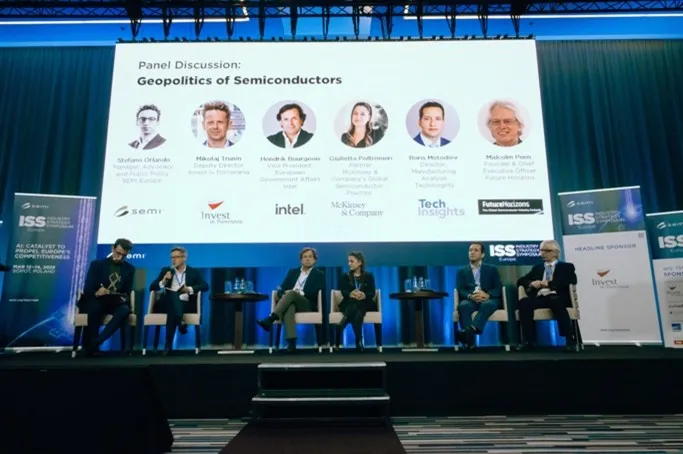
As geopolitical dynamics continue to influence global industries, the semiconductor sector finds itself at a pivotal crossroad. During the SEMI Industry Strategy Symposium (ISS Europe) held in Sopot, Poland, a high-level panel on the Geopolitics of Semiconductors brought together leaders from across the ecosystem to explore Europe’s role in an increasingly fragmented world shaped by strategic dependencies and evolving alliances.Moderated by Stefano Ramundo Orlando, Advocacy Manager at SEMI Europe, the panel convened industry executives, strategic advisors, and policy experts for a forward-looking dialogue on the challenges and opportunities shaping Europe’s semiconductor future.The session opened by acknowledging the rapidly changing geopolitical landscape and its impact on the global semiconductor supply chain. Export controls, investment screening mechanisms, and economic security strategies are no longer abstract policy discussions — they are reshaping investment decisions, manufacturing strategies, and even workforce planning across the globe. While these disruptions present undeniable challenges, panellists underscore that they also mark a pivotal opportunity. For Europe, this is not a moment to retreat but a call to adapt with purpose.Closing the Gaps: Building on Europe’s Strategic AdvantagesGiulietta Poltronieri, Partner at McKinsey Company, mapped out Europe’s strategic position in the global value chain. While Europe boasts global leadership in intellectual property (IP), lithography, and research and development (R D), key gaps remain in foundry capabilities and backend manufacturing. The solution lies not only in plugging these gaps but in securing Europe’s existing strengths — a balancing act between resilience and competitiveness.Giulietta Poltronieri, Partner, McKinsey Company’s Global Semiconductor PracticeMalcolm Penn, Founder CEO of Future Horizons, echoed this sentiment and emphasized that success in semiconductors requires long-term vision and a global mindset. Penn argued that Europe must look beyond its local market, citing Taiwan’s TSMC as a model of how small domestic markets need not constrain global leadership, “The excuse of having no end market in Europe is just an excuse.” Europe, Penn contended, must have the courage to think big and act boldly.Malcolm Penn, Founder Chief Executive Officer, Future Horizons Corporate Strategy Amid UncertaintyHendrik Bourgeois, Vice President of European Government Affairs at Intel, offered insight into how geopolitical risk has become an embedded factor in corporate strategy. Intel’s decision to expand manufacturing in both the U.S. and Europe was directly influenced by a recognition of over-reliance on certain global regions.Bourgeois stressed that while business can adapt to restrictive policy, uncertainty remains the greatest challenge to long-term decision-making. Consistency, trust, and engagement with governments are crucial — and businesses must invest in building political capital just as they do in infrastructure or talent.Hendrik Bourgeois, Vice President, European Government Affairs, Intel China: Partner, Competitor, and Geopolitical PuzzleBoris Metodiev, Director at TechInsights offered a balanced view of China’s role — acknowledging it as both a vital market and a strategic competitor. With nearly 40% of global semiconductor demand and significant state backing, China presents both irresistible opportunity and real systemic risks.Key concerns include technology transfer, the impact of heavy subsidization, and growing market concentration. Addressing these issues, Metodiev suggested, will require a balanced approach focused on diversifying supply chains, protecting intellectual property, and reinforcing trade enforcement — all while maintaining open channels for cooperation and avoiding the pitfalls of full decoupling.Boris Metodiev, Director, Manufacturing Analysis, TechInsights Talent: The Silent BottleneckPanellists identified talent shortages as one of the most yet under-discussed threats to Europe’s semiconductor future. Europe lacks the scale of skilled STEM graduates to meet current and projected demand.Companies like Intel are investing heavily in partnerships with universities and training institutions. However, regulatory obstacles — especially for intra-European mobility of non-EU nationals — remain significant. The call to action was clear: Europe must rethink migration and education policy through the lens of economic strategy, not just under traditional policy frameworks, aligning policy with industrial goals and scaling efforts to match future workforce needs.Central and Eastern Europe: Emerging Pillars of European StrategyThe panel explored how Central and Eastern Europe are increasingly integral to Europe’s semiconductor strategy. Mikołaj Trunin, Deputy Director at Invest in Pomerania, noted that despite geopolitical headwinds, the region continues to attract strong foreign direct investment (FDI). Poland has emerged as a trusted investment destination and a budding semiconductor hub, with Pomerania positioned as a key region for advanced packaging.With nations like Poland taking on higher political and industrial profiles—such as upcoming leadership of the EU Council— the region is positioned to serve as a strategic bridge between Europe’s industrial core and frontier markets. This momentum underscores the importance of embedding these regions more fully into the broader semiconductor ecosystem.Mikołaj Trunin, Deputy Director, Invest in Pomerania A Call for Coordinated ActionThe panel concluded on a note of clarity: geopolitical disruption is not a temporary deviation, but a defining characteristic of the coming industrial era. With semiconductors positioned at the intersection of technology, security, and sovereignty, Europe must act decisively. Companies must continue to evolve, engage politically, and remain agile. To ensure long-term competitiveness and resilience, policymakers and industry leaders must work hand in hand to shape an integrated European semiconductor ecosystem. The stakes are high — but so is the potential.SEMI ContactIranda Chaki, Senior Policy CoordinatorEmail: [email protected]
Read More