

Featuring Executives from Industry Leaders Arm, Cadence, D2S, Keysight, Siemens EDA
MILPITAS, Calif. — March 21, 2022 — Key executives from leading semiconductor EDA and IP companies will gather to discuss the latest industry trends, challenges and opportunities Thursday, April 28, in Santa Clara, California at the annual CEO Outlook hosted by the Electronic System Design Alliance (ESD Alliance), a SEMI Technology Community. Registration is open.
CEO Outlook Panelists
- Anirudh Devgan of Cadence Design Systems
- Niels Fache of Keysight Technologies

- Aki Fujimura of D2S
- Joe Sawicki of Siemens EDA
- Simon Segars of Arm
Semiconductor Engineering editor-in-chief Ed Sperling will moderate the panel.
The in-person event, co-sponsored by Keysight Technologies, will be held at Agilent’s Building 5 at 5301 Stevens Creek Blvd. in Santa Clara, California, beginning at 5:30 p.m. with networking, food and beverages. The hour-long panel starts at 6:30 p.m. and is free for ESD Alliance and SEMI members. Pricing for non-members is $49 per person.
The ESD Alliance Annual Membership meeting for members will be held prior to the start of the CEO Outlook beginning at 5 p.m. Non-members are welcome after registering for the event.
About the Electronic System Design Alliance
The Electronic System Design (ESD) Alliance, a SEMI Technology Community representing members in the electronic system and semiconductor design ecosystem, is a community that addresses technical, marketing, economic and legislative issues affecting the entire industry. It acts as the central voice to communicate and promote the value of the semiconductor design ecosystem as a vital component of the global electronics industry. Visit semi.huihuidehui.workers.dev/en/communities/esda to learn more.
Follow the ESD Alliance
ESD Alliance Bridging the Frontier blog
Twitter: @ESDAlliance
LinkedIn
Facebook
About SEMI
SEMI® connects more than 2,500 member companies and 1.3 million professionals worldwide to advance the technology and business of electronics design and manufacturing. SEMI members are responsible for the innovations in materials, design, equipment, software, devices, and services that enable smarter, faster, more powerful, and more affordable electronic products. Electronic System Design Alliance (ESD Alliance), FlexTech, the Fab Owners Alliance (FOA), the MEMS & Sensors Industry Group (MSIG) and SOI Consortium are SEMI Strategic Technology Communities. Visit semi.huihuidehui.workers.dev to learn more, contact one of our worldwide offices, and connect with SEMI on LinkedIn and Twitter.
All trademarks and registered trademarks are the property of their respective owners.
Association Contact
Nanette Collins
Public Relations for the ESD Alliance
Email: [email protected]
 Wafer fabrication materials and packaging materials revenues in 2021 totaled $40.4 billion and $23.9 billion, respectively, for year-over-year increases of 15.5% and 16.5%. The silicon, wet chemicals, chemical-mechanical planarization (CMP), and photomask segments showed the strongest growth in the wafer fabrication materials market, while packaging materials market growth was largely driven by the organic substrates, leadframes, and bonding wire segments.
 “With hardware security critically important to the semiconductor industry, this project is a great step toward strengthening manufacturing cybersecurity to enable a safe and secure digital life,” said Laith Altimime, president of SEMI Europe. “SEMI welcomes the findings and will address these cybersecurity issues with our members. We thank the SSG research team for its invaluable support and are pleased to have partnered with it on this strategic initiative.”
 Expected to draw hundreds of attendees from across the industry, the 33rd annual ASMC will feature discussions on the global COVID-19 pandemic’s impact on manufacturing leadership, semiconductor market trends, heterogenous integration and quantum computing.







 WiS 2022 builds on the strength of past events with themes including mentorship, career networking and the critical role of companies in promoting gender diversity in the workplace. Industry stakeholders ranging from company leaders, team members and developers of internal programs supporting women will benefit from expert insights, open discussion and networking opportunities at WiS 2022. University STEM students and faculty attending WiS 2022 will learn more about these key workforce development issues and network with industry professionals as the chip industry continues to build its talent pipeline.


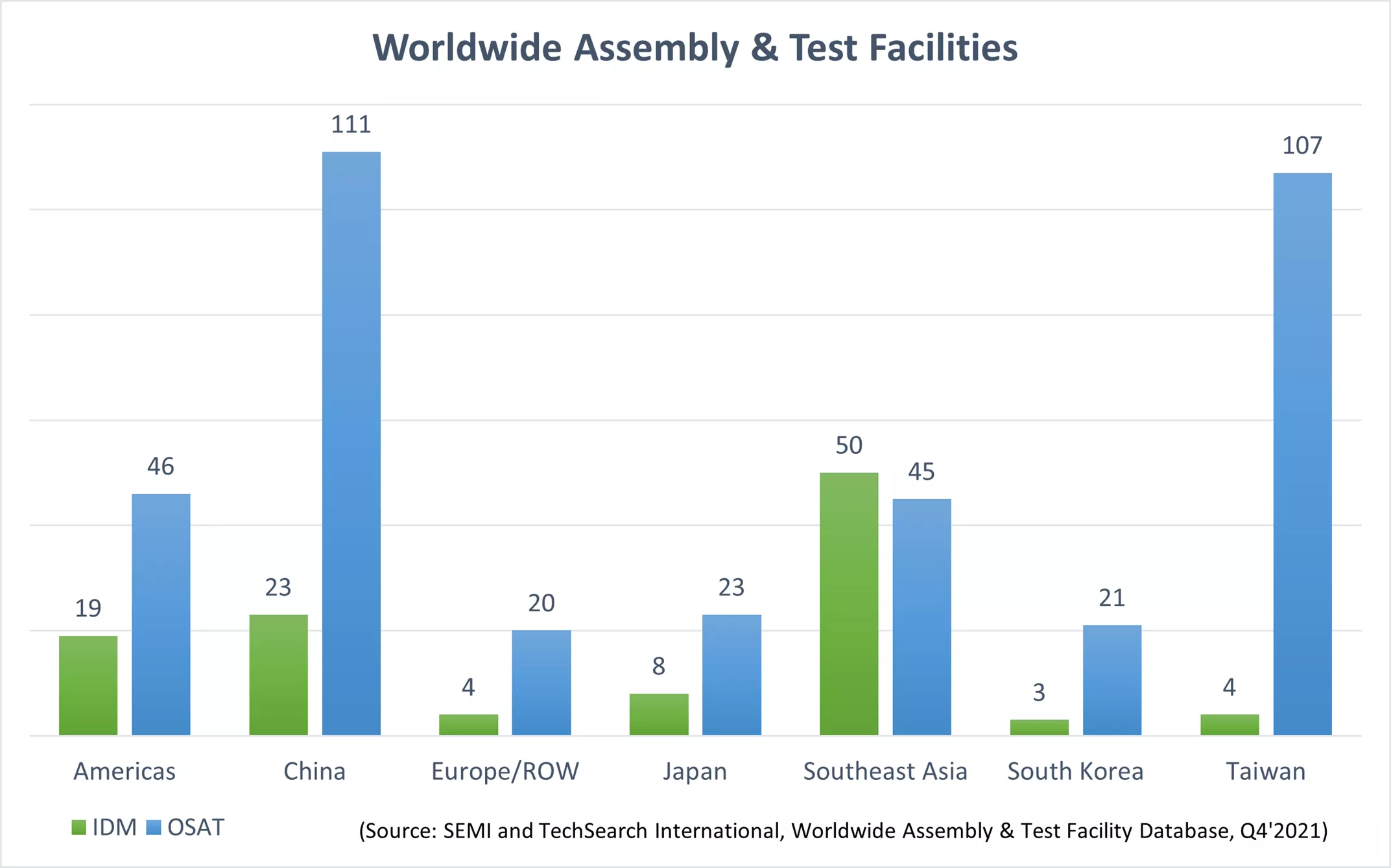
 Formerly known as the Worldwide OSAT Manufacturing Sites Database, the comprehensive database now includes more than 100 updates spanning packaging technology, product specialization and ownership/shareholder. With more than 100 new test facility additions to bring the total number of facilities tracked to 475, the database helps semiconductor manufacturers identify service offerings around the globe, an increasingly important task in supply chain management.
 Sponsored by the SEMI


 Under the act, the European Commission is called to step up investments in Europe’s capabilities to innovate in the design, production and packaging of advanced chips. Additionally, the act aims to strengthen the European Union’s R&D leadership and to address the skills shortages in the region.