downloadGroupGroupnoun_press release_995423_000000 copyGroupnoun_Feed_96767_000000Group 19noun_pictures_1817522_000000Member company iconResource item iconStore item iconGroup 19Group 19noun_Photo_2085192_000000 Copynoun_presentation_2096081_000000Group 19Group Copy 7noun_webinar_692730_000000Path
Skip to main content
Default Banner Image

United States

Regular Pricing

SEMI Members: $75

Non-Members:  $149

SEMI Members: Use your corporate email address during log in to be recognized as a SEMI Member.

Students:  Free

Contact Andreia Smith-Moritz ([email protected]) with a picture of your student ID to receive your discount code.

Belgium France Germany Ireland Italy Japan Taiwan United States masterclass26_recorded_updated.png Business Executive
Highlighted content

In this engaging two-hour Masterclass organized by SEMI, we explore the groundbreaking role of magnetic materials, particularly magnetic nanoparticles (MNPs), in biomedical fields. The session commences with an in-depth review of the physics and synthesis of MNPs, including comprehensive discussions on fundamental theories, synthesis methods, and advanced MNP surface functionalization strategies. Attendees will gain insights into the characterization techniques used to analyze the physicochemical properties of MNPs.

The Masterclass transitions to the applications of MNPs in therapeutic and diagnostic contexts. We will review cutting-edge MNP-based therapies, such as magnetic hyperthermia therapy, targeted drug and gene delivery, and magnetic neurostimulation. In addition, we will discuss various MNP-based diagnostic techniques, including magnetoresistive (MR) sensing, nuclear magnetic resonance (NMR), magnetic particle spectroscopy (MPS), magnetic resonance imaging (MRI), and magnetic particle imaging (MPI). A critical focus of this Masterclass will be on safety and biocompatibility issues associated with the use of MNPs in vivo, examining the toxicity of MNPs, immune responses, and their circulation time in the human body.

The latter part of the session will introduce participants to the innovative field of micromagnetic neural stimulation, an infant yet extremely promising field. We will delve into the design and efficacy of micromagnetic devices, such as the Magnetic Pen (MagPen) and Magnetic Patch (MagPatch) Array, which utilize micrometer-sized coils (μcoils) for targeted neural activation. This is particularly for patients with spinal cord injuries (SCI) and for reducing opioid dependency, with insights drawn from current research supported by the NIH Blueprint Medtech Program. By the end of the Masterclass, attendees will have a comprehensive understanding of the potential clinical applications of MNPs and MEMs-based micromagnetic neurostimulators.


ABOUT THE SPEAKER

Dr. Renata Saha, Senior Scientist, Dupont

Dr. Renata Saha is a Senior Scientist at DuPont located in Wilmington, DE. She holds a PhD in Electrical and Computer Engineering from the University of Minnesota, Twin Cities, which she earned in August 2023. Her undergraduate degree in Electronics & Communication Engineering was obtained from the National Institute of Technology in Durgapur, India. During the summer of 2017, she was an undergraduate research intern at Conseil européen pour la Recherche Nucléaire (CERN), located in Geneva, Switzerland working on the ALICE experiment upgrade.

Dr. Saha is the recipient of 3-year College of Science & Engineering Fellowship, Women in Technology Scholarship 2021-2022 from Cadence Design Systems, and the Graduate Neuromodulation Research Fellowship 2022-2023 from MnDRIVE. She was also elected an iREDEFINE Fellow in 2022 by ECEDHA and was named a Rising Star in EECS. She has published over 30 journal articles, 3 US patents, and 2 book chapters.

Her expertise and research interests involve designing and developing microelectromechanical systems (MEMs) devices for neuromodulation and cardiovascular monitoring, characterizing magnetic nanoparticles (MNPs) for potential biomarkers. Outside of her research and work, Dr. Saha is trained in Indian classical dance form, Odissi, and enjoys performing and choreographing the art form.

United States

Renata Saha
Renata Saha
Senior Scientist
Dupont
Gity Samadi
MODERATOR
Gity Samadi
Sr. Director, R&D Programs
SEMI
NBMC Smart MedTech ESD Alliance FlexTech

In this two-hour Masterclass, Dupont Senior Scientist Renata Saha delves into the biomedical applications of magnetic nanoparticles (MNPs), covering their manufacturing, functionalization as well as therapeutic and diagnostic uses including safety considerations such as biocompatability and toxicology. 

10:00 am - 12:00 pm Off Add to Calendar 2025-10-29 10:00:00 2025-10-29 12:00:00 FEMC #26 Innovations in Magnetic Materials: Applications in Biomedical Engineering In this two-hour Masterclass, Dupont Senior Scientist Renata Saha delves into the biomedical applications of magnetic nanoparticles (MNPs), covering their manufacturing, functionalization as well as therapeutic and diagnostic uses including safety considerations such as biocompatability and toxicology.  United States SEMI.org [email protected] America/Los_Angeles public America/Los_Angeles Watch Now!
Event format
Promote in calendar
Off
United States Image Training

Course Description

The instructor discusses the applied aspects of plasma-assisted etching from a general point of view. The emphasis is on mechanistic understanding. The etching of Si and its compounds is covered in detail. The chemistries used in the etching of other technology-related materials such as Al, organics, and III-V compounds are summarized. Other topics presented include selectivity, loading, ARDE and feature scale problems, damage, and issues associated with high-density plasma RIE. A section on plasma diagnostics and ion-beam based etching methods is briefly discussed. 

Learning Objectives

  • Understand the fundamentals of dry etching and the basic concepts of plasma etching
  • Understand the physics of rf glow discharges (both high and low density)
  • Understand the surface science aspects of RIE including the role of energetic ions
  • Recognize the factors which influence etching anisotropy
  • Define the steps of plasma-surface chemistry leading to etching

Topics Covered

  • Fluorocarbon plasma etching of Si and its compounds
  • Selectivity, loading effects, and aspect ratio dependent etching
  • Uniformity of etching, damage, feature charging issues, and particles
  • Etching of other materials (Al, organics, III-V compounds, etc)
  • Plasma diagnostics such as optical emission spectroscopy with actinometry, mass spectrometry and laser-induced fluorescence
  • Issues in high density plasma etching, wall effects, and ion beam-based methods
  • Deep Reactive Ion Etching (DRIE)
  • Applications and processing etching using ALE
  • End point detection

Who Should Attend

This course is intended for scientists, technicians and others working with or interested in the dry etching of materials in reactive gas glow discharges, particularly those who do not have extensive experience in the field. 

Instructor

Richard Beaudry

PT International, LLC

Instructor Bio
 

Testimonials

See what previous course participants had to say about this training!

  • "Instructors' Process and Hardware knowledge were impressive."
  • "I finally gained a clear understanding of the RIE process."
  • "The instructor had a very good knowledge of the content."
  • "I had a great time to learn fundamental concepts of plasma etching course from SEMI."
  • "The aspect of the course that I found most beneficial was the Bosch processing parameter discussions on profile management. This subject was clearly the expertise of the presenter who skillfully addressed my questions regarding the subject."

Important Information

Note that only the person who registered will receive a certificate of completion. This virtual training will not be recorded. Attendees must be present to access course knowledge. 

Can't find the training link day of? After you register, you will receive the link to the live training via the email address you provided. In addition, you will receive email reminders about 24 hours in an advance and an hour before with the same link. Please keep these emails on hand to access the trainings on time. If you do not see any confirmation emails, please check your junk/spam folders before contacting SEMI U for support.

United States

- SEMI U

This course discusses the fundamentals of plasma assisted phenomena and reactive ion etching (RIE) processes. The emphasis is on the physical and chemical processes that determine the consequences of a reactive gas plasma/surface interaction. The role of energetic ions as encountered in RIE systems is discussed in detail and the factors which influence anisotropy of etching are highlighted. Plasma-assisted etching equipment is described including capacitively coupled, inductively coupled and wave-generated plasmas sources. 

Pricing
  • Members: $745
  • Non-Members: $845

* For group orders with 10+ attendees, and for Students/Veterans discounted pricing, please contact [email protected].

8:00 am - 12:00 pm Off Add to Calendar 2025-10-27 08:00:00 2025-10-28 12:00:00 Plasma Etching, ALE, & RIE (Virtual Training, US & EU) This course discusses the fundamentals of plasma assisted phenomena and reactive ion etching (RIE) processes. The emphasis is on the physical and chemical processes that determine the consequences of a reactive gas plasma/surface interaction. The role of energetic ions as encountered in RIE systems is discussed in detail and the factors which influence anisotropy of etching are highlighted. Plasma-assisted etching equipment is described including capacitively coupled, inductively coupled and wave-generated plasmas sources. PricingMembers: $745Non-Members: $845* For group orders with 10+ attendees, and for Students/Veterans discounted pricing, please contact [email protected]. United States SEMI.org [email protected] America/Los_Angeles public America/Los_Angeles Sold Out
Event format
Promote in calendar
Off
Belgium France Germany Ireland Italy Japan Malaysia Singapore South Korea Taiwan United States Vietnam Image Business Training Featured Speakers

Leverage SEMI U learning offerings to wrap up your 2025 professional development journey! Our pledge remains unwavering: providing comprehensive, technical education to equip you with the skills needed for a prosperous journey in the semiconductor sector.

Are you ready to take your semiconductor industry knowledge to the next level? We're thrilled to invite you to our upcoming webinar titled "SEMI University - 2025 and beyond." This webinar promises to be an informative session where you'll gain insights into the latest updates, exciting live trainings at SEMICON West and virtually the remainder of this year and beyond. 

During this webinar, you can expect to:  

  • Discover the latest updates and enhancements to SEMI U's course catalog.  
  • Learn about the exciting live, in-person training courses scheduled for SEMICON West.
  • Review upcoming virtual instructor-led trainings.
  • Gain access to a special 10% discount on ALL on-demand courses.  


United States

Headshot of Naresh Naik
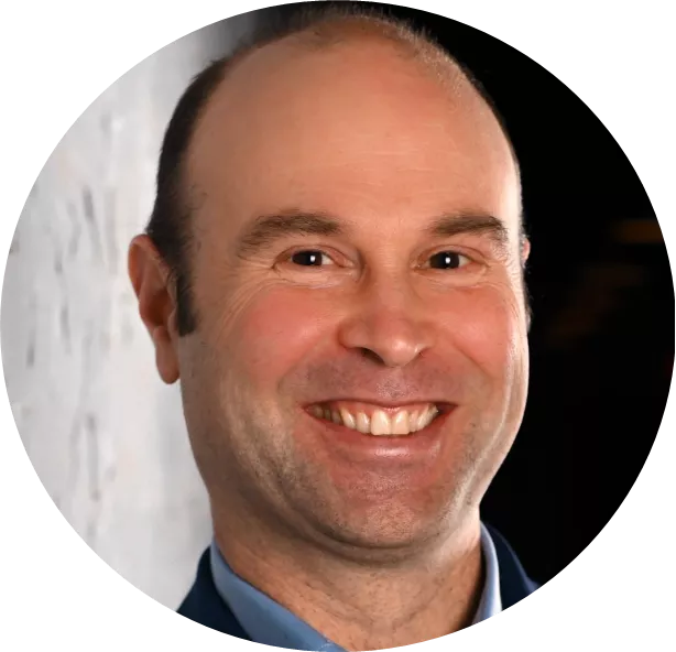
Naresh Naik
Director, SEMI University
SEMI
SEMI U Workforce Development

Join us to discover our current course offerings, upcoming in-person and virtual trainings, and more. Engage in a Q&A session. Plus, by attending this free webinar, you'll receive a 10% discount code for all on-demand courses and will be entered into a raffle to win a FREE course bundle ($100 value). 

Choose your session:

8:00 am - 8:30 am Off Add to Calendar 2025-09-25 08:00:00 2025-09-25 08:30:00 SEMI University - 2025 & Beyond Join us to discover our current course offerings, upcoming in-person and virtual trainings, and more. Engage in a Q&A session. Plus, by attending this free webinar, you'll receive a 10% discount code for all on-demand courses and will be entered into a raffle to win a FREE course bundle ($100 value). Choose your session:US/EU: 8:00 AM – 8:30 AM PT [Register Now]Asia/US: 5:00 PM – 5:30 PM PT [Register Now] United States SEMI.org [email protected] America/Los_Angeles public Register Now
Event format
Promote in calendar
Off

SEMI Members:  $75

Use your corporate email address during log in to be recognized as a SEMI Member.

Non-Members:  $149

Students:  Free

Contact Andreia Smith-Moritz ([email protected]) with a picture of your student ID to receive your discount code.

Belgium Germany Singapore Taiwan United States FEMC 25 Recorded Tile Business Executive Technical
Highlighted content

Graphenea: Graphene Device Manufacturing

Graphene, a two-dimensional material with extraordinary electrical, mechanical, and biocompatible properties, is emerging as a key enabler for the next generation of medical devices. In this presentation, we will explore how Graphenea, through its advanced Graphene Foundry services, is driving the integration of graphene into scalable device manufacturing for biomedical applications. Attendees will gain insight into our end-to-end fabrication capabilities, from graphene synthesis, wafer-scale CVD graphene growth to cleanroom device prototyping and packaging. We will showcase examples of graphene-based biosensors, flexible electronics, and neural interfaces developed through our foundry platform, emphasizing their potential impact in diagnostics, monitoring, and therapeutic applications. The session will also address the challenges of material integration, process scalability, and regulatory pathways for graphene in medical technologies, providing a practical roadmap for researchers and companies looking to bring graphene-enabled devices from lab to market.

INBRAIN: Pioneering Precision Neuroelectronics: From Materials to Scalable Therapies

The convergence of materials science, artificial intelligence, and neuromodulation is transforming the future of neuroscience. This talk explores how high-density graphene-based brain-computer interfaces are enabling real-time decoding and precision modulation of neural circuits. Carolina Aguilar, CEO and Co-Founder of INBRAIN Neuroelectronics, will present the technological and clinical journey behind the world’s first graphene neural interface in humans, and how this platform is designed to deliver adaptive, patient-specific therapies for neurological disorders such as Parkinson’s disease. The session will highlight the translational path from research to regulated medical devices, and the role of Europe in leading responsible innovation in neurotechnology

ABOUT THE SPEAKERS:

Jesús de la Fuente

Jesús de la Fuente is the founder and CEO of Graphenea, a leading graphene production company established in 2010. Before founding Graphenea, he served as a Manager at Arthur Andersen, Director at PricewaterhouseCoopers in advisory professional services, and Managing Director at an industrial materials distribution company. He holds a Bachelor of Science in Engineering from Deusto University and an Executive MBA from IESE Business School. Under his leadership, Graphenea has become a world-leading graphene producer, contributing to the development of graphene applications across various sectors in over 60 countries.

Carolina Aguilar

Carolina Aguilar is the CEO and Co-Founder of INBRAIN Neuroelectronics, a neurotechnology company pioneering the use of graphene-based brain-computer interfaces for precision neuromodulation. With over 20 years of experience in healthcare, including 13 years at Medtronic where she led global businesses in brain modulation and diabetes, she has built a career at the intersection of innovation, neuroscience, and impact. Under her leadership, INBRAIN achieved the first-in-human implantation of a graphene neural interface and received FDA Breakthrough Device Designation. Carolina is also a 2025 World Economic Forum Technology Pioneer and a strong advocate for responsible, human-centric deep tech in Europe for the world.

United States

Jesús de la Fuente
Jesús de la Fuente
CEO
Graphenea
Carolina Aguilar
Carolina Aguilar
CEO and Co-Founder
INBRAIN
Gity Samadi
MODERATOR
Gity Samadi
Sr. Director, R&D Programs
SEMI
NBMC Smart MedTech FlexTech

Join us for this exciting Master Class with Jesús de la Fuente, Founder and CEO of Graphenea, and Carolina Aguilar, CEO and Co-Founder of INBRAIN, as they showcase their pioneering efforts of integrating graphene into scalable medical devices highlighting advancements in various medtech applications including biosensors and neural interfaces.

9:00 am - 11:00 am Off Add to Calendar 2025-09-10 09:00:00 2025-09-10 11:00:00 FEMC#25 Enabling Next-Generation Medical Devices: Graphene Device Manufacturing Join us for this exciting Master Class with Jesús de la Fuente, Founder and CEO of Graphenea, and Carolina Aguilar, CEO and Co-Founder of INBRAIN, as they showcase their pioneering efforts of integrating graphene into scalable medical devices highlighting advancements in various medtech applications including biosensors and neural interfaces. United States SEMI.org [email protected] America/Los_Angeles public Watch Now!
Event format
Promote in calendar
Off
United States Image Training

Don't miss this chance to grow your knowledge, build your network, and accelerate your journey in the semiconductor industry.  


Course Options: 

PFAS Compounds in Semiconductor Environment: Half Day Course

  • Per- and Polyfluoroalkyl substances (PFAS) are a group of over 15,000 compounds which have been used in a variety of different industries due to their unique properties. Over the past two decades, their presence in water and the human body has become of increasing concern, with studies linking certain PFAS to adverse effects in the organisms studied. This has led to increasing consumer awareness, litigation, and the regulation of PFAS compounds. This course provides an in-depth review of PFAS compounds, their history, market drivers, regulations, current uses in the semiconductor industry, and methods for sampling and analysis, over the entire semiconductor value chain.

Semiconductor Device Manufacturing in a Cleanroom (Best Practices to Improve Product Reliability and Yield)

  • This course is designed for people who utilize cleanrooms. Semiconductor device manufacturing is a complex process that involves working in a cleanroom with a wide range of specialized equipment and materials. Many challenges must be overcome to meet production goals. This course provides the fundamentals and thought processes to improve your production reliability and yield. This course is intended for mechanical engineers, process engineers, test engineers, quality assurance engineers, and technicians.

Overview of Semiconductor Manufacturing

  • This course offers a solid foundation in semiconductor manufacturing, from basic concepts to advanced techniques, providing practical insights into the tools, processes, and technologies driving the industry.

Phoenix Convention Center
100 N 3rd St
Phoenix, AZ 85004
United States

SEMI U

Finish your show experience with SEMI U training sessions! 

Learn from experienced industry leaders across a wide range of topics. Choose a course that aligns with your goals and gain valuable insights to advance your role in the dynamic world of semiconductors.

Following the overwhelming success of last year’s inaugural trainings—where 125+ industry professionals, both seasoned and new, participated in five pre-show sessions—we’re expanding! This year, we’re offering three sessions the last day of the show to meet the growing training demand as the industry’s talent gap continues to widen. 


8:00 am - 4:00 pm Off Add to Calendar 2025-10-09 08:00:00 2025-10-09 16:00:00 Trainings at SEMICON West Finish your show experience with SEMI U training sessions! Learn from experienced industry leaders across a wide range of topics. Choose a course that aligns with your goals and gain valuable insights to advance your role in the dynamic world of semiconductors.Following the overwhelming success of last year’s inaugural trainings—where 125+ industry professionals, both seasoned and new, participated in five pre-show sessions—we’re expanding! This year, we’re offering three sessions the last day of the show to meet the growing training demand as the industry’s talent gap continues to widen.   Phoenix Convention Center 100 N 3rd St Phoenix, AZ 85004 United States SEMI.org [email protected] America/Phoenix public America/Phoenix Register Now
Event format
Promote in calendar
Off
United States Image Training

Don't miss this chance to grow your knowledge, build your network, and accelerate your journey in the semiconductor industry.  


Course Options: 

Advanced Packaging (Chiplets, WLP, Flip Chip, 3D Stacking)

  • This 1-day course addresses IC packaging, assembly, and package/substrate interconnections. It stresses the impact of the IC and end product requirements, i.e., “smaller, better, cheaper” their influence on the manufacturing processes. Topics include area packaging- ball grid arrays, flip chip, fanout, stacking die and chip scale packages, and the assembly technologies – chip & wire, tape automated bonding, and flip chip, as is emerging technologies namely, 3-D and stacked die, and packaging reliability issues.

Basic Electronics & Troubleshooting

  • This course provides students with a fundamental understanding of electronics and troubleshooting techniques. Topics covered include current, voltage, resistors, capacitors, inductors, diodes, and transistor fundamentals. Students will learn to differentiate between AC and DC power, understand digital and analog circuits, and interpret electronic component datasheets.  The course offers a comprehensive overview of the theory, operation, and applications of essential testing equipment, including the Volt-Ohm-Meter, Digital Multi-Meter, and Oscilloscope. Through hands-on training, students will build breadboard circuits and develop troubleshooting skills using multi-meters.

Fundamentals of Atomic Layer Deposition (ALD)

  • Discover how atomic-scale precision is revolutionizing semiconductor manufacturing with Atomic Layer Deposition (ALD) and Etching (ALE). This course provides a practical introduction to Atomic Layer Deposition, an essential technique in semiconductor manufacturing. You'll learn about ALD foundational concepts including growth, advantages, measurements, and more, chemical precursors for use in ALD, selected ALD processes, area-selective deposition, and atomic layer etching. Overall, the applications and chemistry used in semiconductor processing as it relates to ALD and ALE are heavily discussed.

Fundamentals of EUV

  • This course provides attendees with an overview of the fundamentals, current status, and technical challenges of EUV Lithography. The course will begin with a review of lithography in general drawing parallels between EUV and DUV lithography. The course will then go on to review EUV specific challenges/solutions including sources (lithography and metrology), optics, metrology, masks, and patterning materials. Two areas where EUV specific challenges are particularly significant are patterning materials and photomasks; this course will cover these two areas in more detail including topics such as resist stochastics, radiation chemistry, reflective thick masks, off-axis mask illumination, phase shift masks, and mask stochastics.

Fundamentals of Microsystems (MEMs) Fabrication and Applications

  • This introductory course is designed to educate people from any background that are new to Microsystems Fabrication and Applications, no prior knowledge is expected. We begin with some historical applications to set the stage for diving into how these devices are made.

Plasma Etching, ALE, & RIE

  • This course discusses the fundamentals of plasma assisted phenomena and reactive ion etching (RIE) processes. The emphasis is on the physical and chemical processes that determine the consequences of a reactive gas plasma/surface interaction. The role of energetic ions as encountered in RIE systems is discussed in detail and the factors which influence anisotropy of etching are highlighted. Plasma-assisted etching equipment is described including capacitively coupled, inductively coupled and wave-generated plasmas sources. The instructor discusses the applied aspects of plasma-assisted etching from a general point of view. The emphasis is on mechanistic understanding. The etching of Si and its compounds is covered in detail. The chemistries used in the etching of other technology-related materials such as Al, organics, and III-V compounds are summarized. Other topics presented include selectivity, loading, ARDE and feature scale problems, damage, and issues associated with high-density plasma RIE. A section on plasma diagnostics and ion-beam based etching methods is briefly discussed.

Understanding Semiconductor Technology & Business

  • The first part of the course provides a brief overview of semiconductor design and fabrication steps, encompassing IC design techniques, all wafer processing steps, assembly, and packaging. It delves into semiconductor jargon in laypeople terms, and various substrate types such as Si, SiGe, FDSOI, GaAs, SiC, GaN. Additionally, it discusses different types of transistors like pMOS, nMOS, Bipolar, BiCMOS, CMOS, FinFets, and GAA and their evolution and what applications they are used in. The second part of the course focuses on semiconductor business aspects such as silicon economics, wafer processing costs, semiconductor revenue forecasts, driving forces in the industry, top semiconductor IDMs, market competitors based on market share, OEMs, foundries, top tool vendors, and Fabless companies. Addresses the fastest-growing semiconductor markets based on geographic locations and applications, identifies semiconductor competitors/customers, and discusses major semiconductor markets like Automotive, PC, Mobile, Memory, Wireless, Cell phones, Consumer, Gaming, AI, IoT, Digital TV, Radio, Automotive, MEMS, and Emerging Technology & Impact on Industry.

Wet Processing in the Semiconductor Industry

  • This one-day course provides a working knowledge of surface conditioning and cleaning techniques used in the manufacture of integrated circuits. Fundamentals of the techniques used for cleaning the wafer surface will be discussed. Practical applications and methods for cleaning will be presented. Upon completing this course participants will have an understanding of all types of cleaning processes used in IC manufacturing; surface conditioning for pre-diffusion clean, in particular pre-gate oxide clean, post-etch and post-implant photoresist removal, particle removal, post-CMP clean. Participants will be able to understand the cleaning roadmaps and limitations of clean technologies as the node sizes decrease. The course participant should be able to make informed decisions on the surface conditioning and cleaning processes and techniques to utilize for IC manufacturing. Course topics include surface conditioning and cleaning technologies, processes and equipment, wet, plasma, and dry cleaning, surface conditioning and cleaning techniques, cleaning technologies, effects, and challenges.

Phoenix Convention Center
100 N 3rd St
Phoenix, AZ 85004
United States

SEMI U

Start your show experience with SEMI U training sessions! 

Learn from experienced industry leaders across a wide range of topics. Choose a course that aligns with your goals and gain valuable insights to advance your role in the dynamic world of semiconductors.

Following the overwhelming success of last year’s inaugural trainings—where 125+ industry professionals, both seasoned and new, participated in five pre-show sessions—we’re expanding! This year, we’re offering eight sessions the day before the show to meet the growing training demand as the industry’s talent gap continues to widen. 


8:30 am - 5:30 pm Off Add to Calendar 2025-10-06 08:30:00 2025-10-06 17:30:00 Pre-Show Trainings at SEMICON West Start your show experience with SEMI U training sessions! Learn from experienced industry leaders across a wide range of topics. Choose a course that aligns with your goals and gain valuable insights to advance your role in the dynamic world of semiconductors.Following the overwhelming success of last year’s inaugural trainings—where 125+ industry professionals, both seasoned and new, participated in five pre-show sessions—we’re expanding! This year, we’re offering eight sessions the day before the show to meet the growing training demand as the industry’s talent gap continues to widen.   Phoenix Convention Center 100 N 3rd St Phoenix, AZ 85004 United States SEMI.org [email protected] America/Phoenix public America/Phoenix Register Now
Event format
Promote in calendar
Off

Pfeiffer Vacuum+Fab Solutions – a member of the global Busch Group – presents the CenterLine CNR series, an expansion to the existing CenterLine family of vacuum gauges, particularly suited for the harsh operating conditions in the semiconductor industry.

Asslar, May 16, 2025 – The CenterLine CNR series consists of analog capacitive vacuum gauges that can measure over four decades in the full scale between 0.1 and 1000 Torr. Available in heated and unheated variants, the CNR series expands the existing CenterLine product family and delivers reliable measurements even under the harshest operating conditions. Just like the other CenterLine gauges, the CNR series provides an optimal cost–performance ratio and allows for easy integration into existing installations with measurement technology from other manufacturers.

CNR gauges are ideally used in combination with pressure control valves and can be employed for a wide range of applications in the semiconductor industry, such as dry etching, CVD and ALD processes. They can also be implemented for analytics, R&D, and various other industries. In this expansion to the product series, five different versions are available: the 36x, 37x, 38x, 39x and 30x. All products in the series are SEMI S2 compliant.

For processes at every temperature

The CenterLine CNR series provides a variety of options for processes at different temperatures. The 36x is an unheated variant for reliable measurements at ambient temperature with an accuracy of 0.2%. Self-heating versions are also available at 45, 100, 160 and 200 °C. The 45 °C variant provides an accuracy of 0.15%, making it excellent for calibration laboratories and high-quality control. With an accuracy of 0.4%, the other self-heating versions allow higher accuracy of readings in high-temperature or hot gas processes than comparable gauges.

Resistance to contamination and corrosion

A diaphragm sensor forms the heart of the measurement device. It is protected by a stable and resistant ceramic shield coated through atomic layer deposition

(ALD). The shield protects the sensor both from exposure to the high temperatures of the process gases and from potential corrosion. This ultimately ensures higher reliability and accuracy as well as a longer sensor life, even under harsh plasma, due to minimized contamination. As sensor drift is also reduced, calibration is required less frequently and thus the overall cost of ownership is lowered.

Pressure control (p-control) filter setting

The gauges in the CenterLine CNR series are equipped with a special filter setting known as “p-control,” or pressure control. This is designed to be fast and adaptive, enabling the gauge to respond more quickly to pressure changes as well as provide accurate and smooth pressure control. This feature is particularly effective in combination with a pressure control valve.

The new CenterLine CNR series of vacuum gauges provides reliable measurement over 4 decades in the full scale of 0.1 – 1000 Torr at various self-heating temperature levels. Source: Pfeiffer Vacuum+Fab Solutions.

About the Busch Group

The Busch Group is one of the world’s largest manufacturers of vacuum pumps, vacuum systems, blowers, compressors and gas abatement systems. Under its umbrella, the group houses two well-known brands: Busch Vacuum Solutions and Pfeiffer Vacuum+Fab Solutions. The gas abatement systems previously offered by centrotherm clean solutions – a former Busch Group brand – are now part of the Pfeiffer portfolio. The extensive product and service offer includes solutions for vacuum, overpressure and abatement applications in all industries, such as food, semiconductors, analytics, chemicals and plastics. This also includes the design and construction of tailor-made vacuum systems and a worldwide service network. The Busch Group is a family business that is managed by the Busch family. More than 8,000 employees in 44 countries worldwide work for the group. Busch is headquartered in Maulburg, Baden-Württemberg, in the tri-country region of Germany, France and Switzerland. The Busch Group manufactures in its 23 own production plants in China, the Czech Republic, France, Germany, India, Romania, South Korea, Switzerland, the United Kingdom, the USA and Vietnam. The Busch Group has an annual consolidated revenue of close to 2 billion Euro.

Media Contact Pfeiffer Vacuum+Fab Solutions Sandra Thirtle-Höck Head of Internal Communications Berliner Strasse 43 35614 Asslar, Germany

+49 (0)6441 802 – 1460 [email protected]

www.pfeiffer-vacuum.com www.buschgroup.com

Test Research, Inc. (TWSE: 3030), the leading test and inspection systems provider for the electronics manufacturing industry, is proud to announce its successful partnership with Bosch in the development of an AI visual check solution for MEMS packaging.

Bosch has recognized TRI's valuable contribution to their success in MEMS packaging in 2025 with a Certificate of Appreciation. The certificate acknowledges the successful completion of the AI visual check for MEMS packaging, highlighting the strong cooperation and partnership between the two companies.

This collaboration demonstrates TRI's expertise in AI-driven inspection solutions and its commitment to providing valuable solutions for the electronics manufacturing industry. TRI's AI-powered solutions include the AI Defect Detection, AI Smart Programming, AI Verify Host, AI training tool, AI Station, and more.

Please visit the following link to learn more about TRI's AI Solutions:
https://www.tri.com.tw/en/about/about-107-2-2.html

Learn more about the Bosch Group by following the link below:
https://www.bosch-presse.de/pressportal/de/en/company-page.html

###

About Test Research, Inc. (TRI)

TRI (TWSE: 3030), offers the most robust product portfolio in the industry for Automatic Test and Inspection solutions. Learn more at http://www.tri.com.tw. For sales and service information, please write to us at [email protected] or call +886-2-2832 8918.

Stanton Chase is pleased to announce that Sundar Rajan Ramalingam has joined the firm as a Partner in North America. His addition strengthens the firm's executive search and leadership consulting capabilities for the semiconductor sector at a time of rapid transformation.

Sundar brings nearly three decades of leadership experience across manufacturing and global technology sectors. He has scaled a multi-billion-dollar global engineering division and supported the growth of several Global Capability Centers (GCCs). Within the semiconductor ecosystem, he has played a pivotal role in building and advising leadership teams across chip design, chip-to-cloud platforms, semiconductor fabs, and foundry operations.

This deep operational and strategic background gives Sundar a unique perspective on the evolving talent needs of semiconductor organizations.

"The semiconductor industry is entering a pivotal era—what I call a 'perfect leadership storm'—driven by generative AI, strategic autonomy imperatives, and breakthroughs like 3nm and advanced packaging," said Sundar. "While these trends are accelerating innovation, the industry also faces a growing talent gap. Companies need capable leaders who can navigate complexity, scale innovation, and build resilient teams. I plan to use my experience in technology and manufacturing to help semiconductor companies find executives who deliver results and foster sustainable growth."

Sundar's career spans both strategic HR leadership and general management with P&L responsibility, offering clients a rare blend of technical insight and leadership development expertise.

"Sundar fits well with our North American team and fills a specific need in our practice," said Mickey Matthews, Managing Director at Stanton Chase in North America and Chair of the Governance Committee. "His time working across borders gives him a genuine understanding of how global teams function. Blending this multicultural understanding with Sundar's deep technology products and services vertical expertise matters a lot to the clients we serve and specifically in the semiconductor space."

Jan-Bart Smits, Managing Partner at Stanton Chase Amsterdam and Global Sector Leader for Semiconductors, added: "Sundar joins us when the semiconductor industry sits at a turning point. Firms in this sector are looking for something different in their executives—people who understand both market forces and engineering details. Sundar knows this world and will further enhance our ability to serve chip makers and their suppliers."

As the semiconductor industry moves into a new chapter—marked by AI-driven demand, geopolitical shifts, and the race toward next-gen nodes—Sundar's appointment signals Stanton Chase's commitment to helping clients lead with confidence and clarity.

Sundar holds an MBA from XLRI Jamshedpur (India) and completed executive education programs, including the Chief Human Resource Officer Program at Wharton, University of Pennsylvania.

He will serve clients from Stanton Chase offices in Baltimore and Raleigh, USA, as well as Bangalore, Hyderabad, and Chennai, India—locations near semiconductor business centers.

Click here to learn more about Sundar.

Click here to learn more about Stanton Chase's semiconductor expertise.

About Stanton Chase

Stanton Chase ranks among the top global retained executive search firms with more than 76 offices in 45 countries and a worldwide team of senior consultants. Stanton Chase serves clients across multiple industry specialties and places C-suite executives, senior managers, and board members for companies ranging from global corporations to emerging businesses. Stanton Chase belongs to the Association of Executive Search and Leadership Consultants (AESC), adhering to the highest industry standards of professionalism and ethics.

United States noel tech graphic Technical
Highlighted content


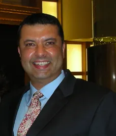
Ardy Sidhwa, Ph.D., CTO, Noel Technologies

Dr. Sidhwa has over 25 years of innovative contributions to semiconductor device manufacturing and processing development.  His expertise includes Mergers and Acquisitions, Semiconductor processing and characterization, Nanotechnology, R&D, Capital equipment sourcing, Devices Characterization and Yield Enhancement, Semiconductor Fab constructions, Semiconductor silicon wafer reclaim, Equipment parts cleaning using novel surface cleaning methods, Lean manufacturing, Quality control, Materials characterization, Sustainability, Design of Solar Cells and Composite Armor Manufacturing for the US government.  In addition, he is proficient in technology development for strategic alliances and multiple joint ventures.  Dr. Sidhwa has 7 U.S. patents issued, two pending applications in multidisciplinary fields, and over 100 publications.

Dr. Sidhwa has led teams to successfully deliver numerous technologies through a complete product development lifecycle, from early R&D to end customer deployment and qualification. He excels at troubleshooting endemic technical manufacturing process integration and reliability issues through systematic and thorough investigation. His hands-on problem-solving skills have repeatedly been demonstrated at startups and established companies by rapidly delivering qualified products to the market.

United States

MSIG

Hosted by SEMI MSIG

Innovative Lab to Fab Semiconductor Processes: Advancing sensing, smart manufacturing, and biomedical applications

Emerging MEMS and sensor technologies demand both advanced process capabilities and robust pathways to volume manufacturing. NOEL Technologies, a Silicon Valley MEMS foundry, brings decades of expertise in microfabrication – from state-of-the-art lithography and deep etching to thin-film deposition and multi-layer integration. Its versatile fabrication facility supports wafer diameters ranging from 50 mm up to 300 mm, enabling prototyping on small substrates as well as scale-up to full 300 mm production. NOEL’s engineers excel at integrating novel materials and processes to create structures that often lack a conventional manufacturing path, while handling complex builds with multiple mask layers with both wet and plasma etching of silicon, dielectrics, and metals. Through a proven “Lab-to-Fab” approach, NOEL serves as a vital bridge from R&D to high-volume fabrication, accelerating the transition of innovative designs from the laboratory to the fab floor.

Recent collaboration through Pure Wafer’s acquisition of NOEL Technologies has further expanded these capabilities. Pure Wafer, a leading U.S. provider of high-purity silicon wafer solutions, adds in-house supply of prime silicon substrates (50 mm–300 mm) and an extensive portfolio of exotic dielectric and metal thin films. By coupling NOEL’s proprietary MEMS processes with Pure Wafer’s materials expertise, the combined team delivers a “complete silicon solution” that enhances device performance and yield for next-generation sensors. This synergy is enabling cutting-edge sensor technologies in IoT, biomedical, and industrial applications, supported by faster prototyping cycles and a streamlined path to market. Equally important, the integration provides key business advantages – from cost efficiencies via comprehensive on-shore services (e.g., wafer reclaim and reuse) to improved supply chain resilience through a domestic source for critical materials and fabrication.

This presentation will showcase how the NOEL–Pure Wafer partnership supports next-generation sensor innovation in alignment with the key industry tracks driving future advancements in IoT, Intelligent Sensing, Advanced embedded system Technologies, Multi-Sensor capabilities, Smart Manufacturing, and biomedical applications. By leveraging Pure Wafer and NOEL Technologies' expertise, MEMS and sensor innovators can achieve superior device performance, faster prototyping, and scalable production solutions. This collaboration is paving the way for next-generation innovative sensing solutions that drive technological breakthroughs across industries.

8:00 am - 9:00 am Off Add to Calendar 2025-06-11 08:00:00 2025-06-11 09:00:00 Innovative Lab to Fab Semiconductor Processes: Advancing sensing, smart manufacturing, and biomedical applications Hosted by SEMI MSIGInnovative Lab to Fab Semiconductor Processes: Advancing sensing, smart manufacturing, and biomedical applicationsEmerging MEMS and sensor technologies demand both advanced process capabilities and robust pathways to volume manufacturing. NOEL Technologies, a Silicon Valley MEMS foundry, brings decades of expertise in microfabrication – from state-of-the-art lithography and deep etching to thin-film deposition and multi-layer integration. Its versatile fabrication facility supports wafer diameters ranging from 50 mm up to 300 mm, enabling prototyping on small substrates as well as scale-up to full 300 mm production. NOEL’s engineers excel at integrating novel materials and processes to create structures that often lack a conventional manufacturing path, while handling complex builds with multiple mask layers with both wet and plasma etching of silicon, dielectrics, and metals. Through a proven “Lab-to-Fab” approach, NOEL serves as a vital bridge from R&D to high-volume fabrication, accelerating the transition of innovative designs from the laboratory to the fab floor.Recent collaboration through Pure Wafer’s acquisition of NOEL Technologies has further expanded these capabilities. Pure Wafer, a leading U.S. provider of high-purity silicon wafer solutions, adds in-house supply of prime silicon substrates (50 mm–300 mm) and an extensive portfolio of exotic dielectric and metal thin films. By coupling NOEL’s proprietary MEMS processes with Pure Wafer’s materials expertise, the combined team delivers a “complete silicon solution” that enhances device performance and yield for next-generation sensors. This synergy is enabling cutting-edge sensor technologies in IoT, biomedical, and industrial applications, supported by faster prototyping cycles and a streamlined path to market. Equally important, the integration provides key business advantages – from cost efficiencies via comprehensive on-shore services (e.g., wafer reclaim and reuse) to improved supply chain resilience through a domestic source for critical materials and fabrication.This presentation will showcase how the NOEL–Pure Wafer partnership supports next-generation sensor innovation in alignment with the key industry tracks driving future advancements in IoT, Intelligent Sensing, Advanced embedded system Technologies, Multi-Sensor capabilities, Smart Manufacturing, and biomedical applications. By leveraging Pure Wafer and NOEL Technologies' expertise, MEMS and sensor innovators can achieve superior device performance, faster prototyping, and scalable production solutions. This collaboration is paving the way for next-generation innovative sensing solutions that drive technological breakthroughs across industries. United States SEMI.org [email protected] America/Los_Angeles public America/Los_Angeles Register
Event format
Promote in calendar
Off