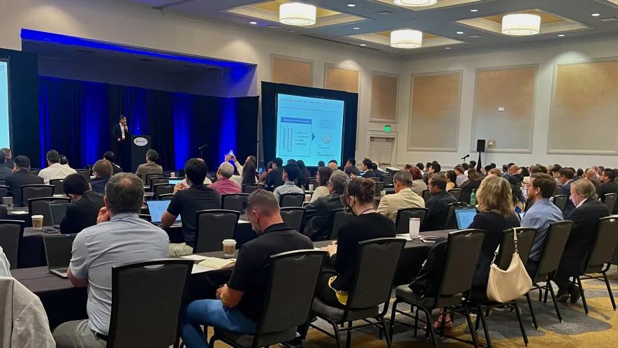
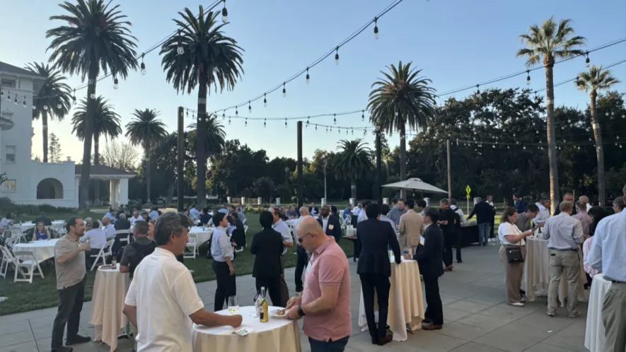
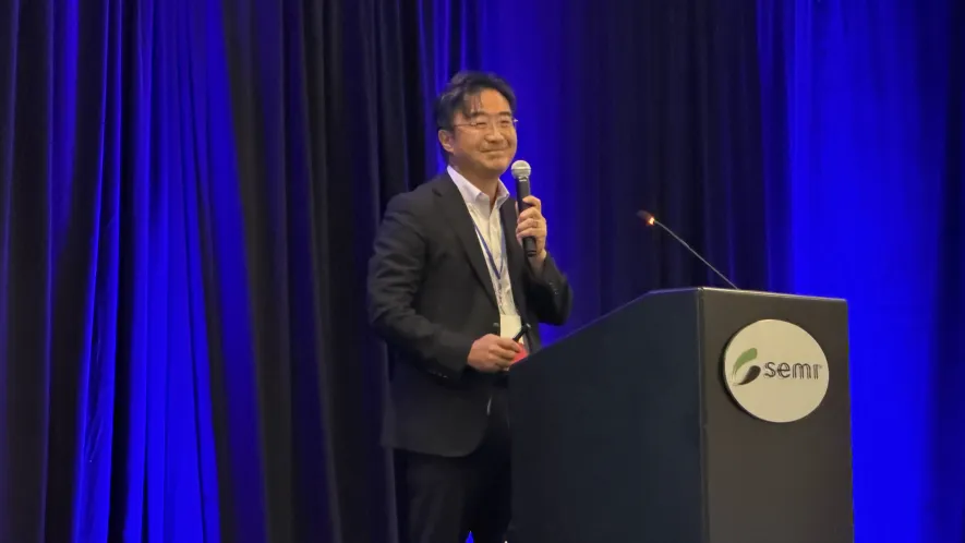
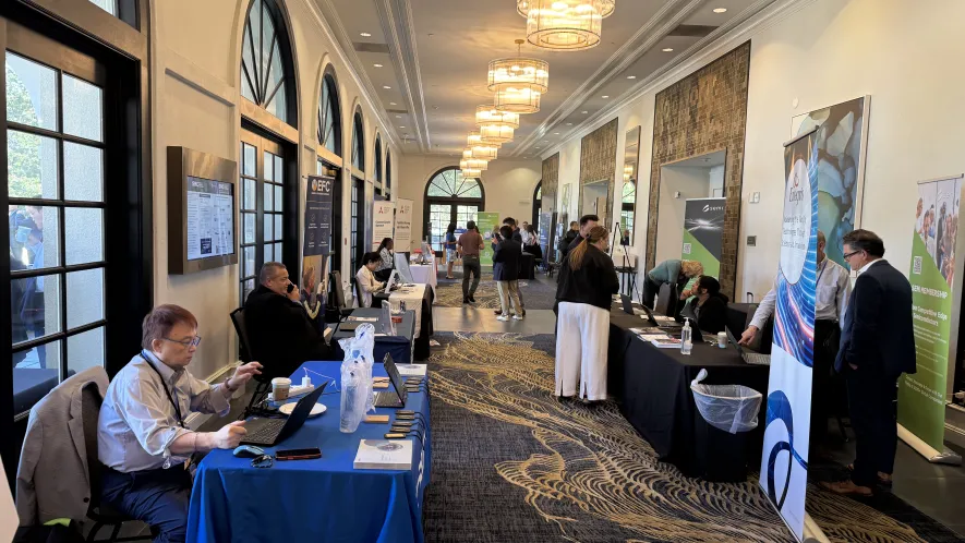
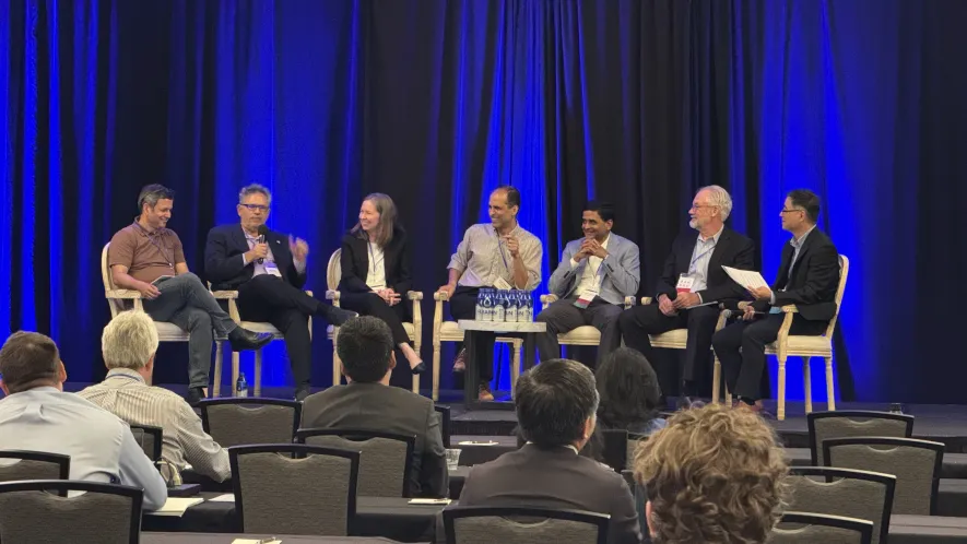
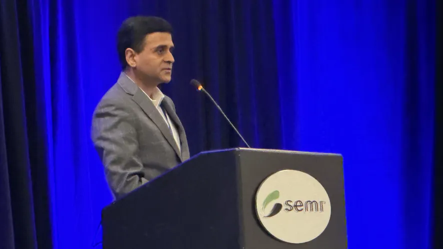
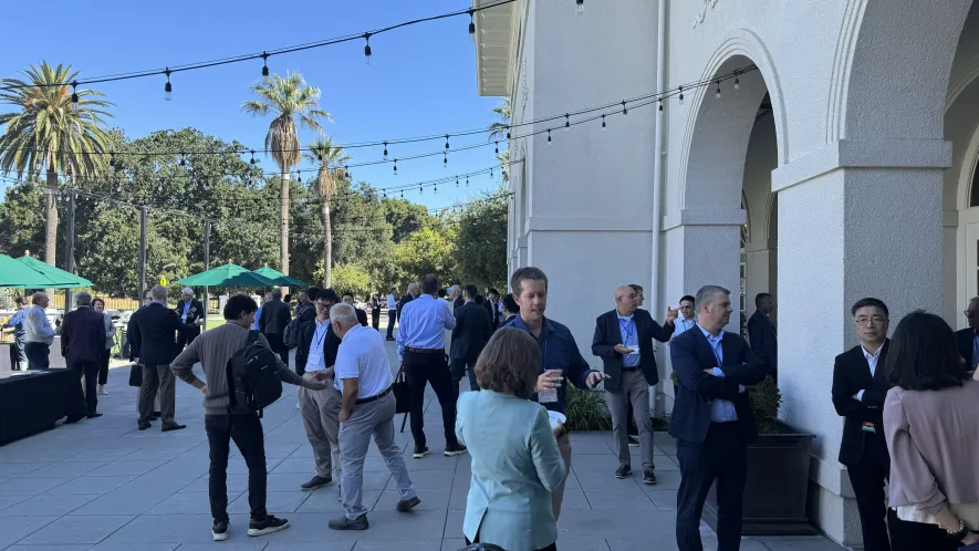
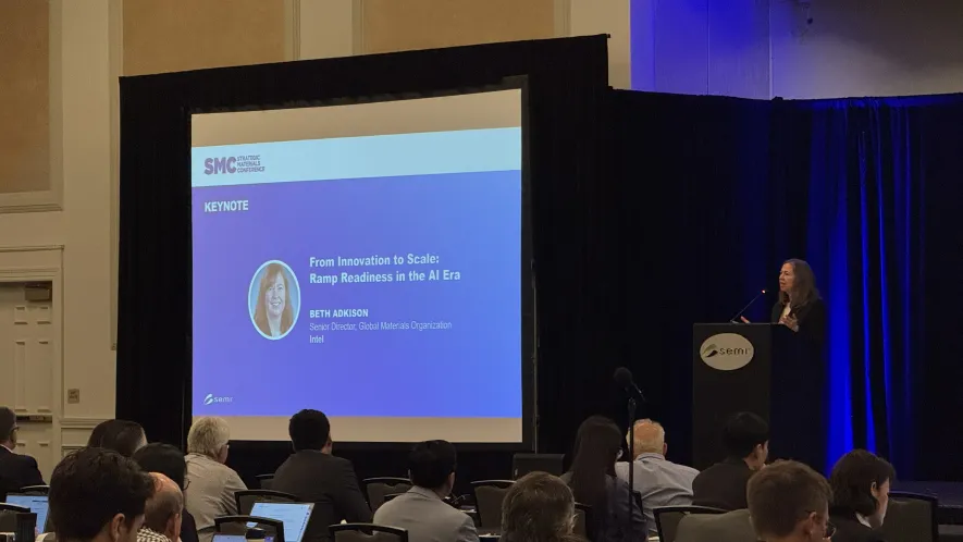
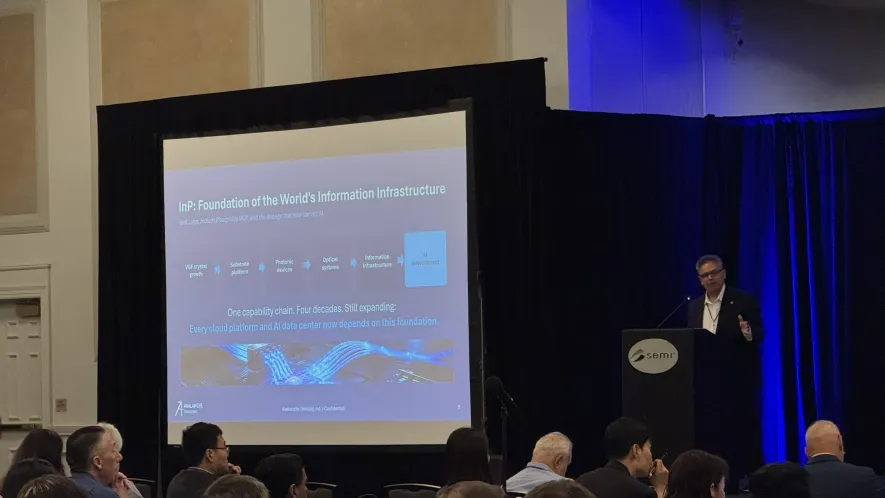
Align your company with the ASMC, one of the most highly respected semiconductor manufacturing conferences in the industry. The attendees are an excellent audience to expand your brand image to new and existing markets.
CONTACT
Shane Poblete Director, Sales & Business Development - Expo and Events, SEMI Tel: +1 202-847-5983 Email: [email protected]
Media Sponsors
SEMI is proud to partner with the following media to bring you news about this event. Click below to visit their website to learn more about each of them.
Save the dates for ASMC 2027—June 14–17!
Advancing Semiconductor Manufacturing Excellence
ASMC is the leading international technical conference for discussing solutions that improve the collective manufacturing expertise of the semiconductor industry. Solving the challenges presented by semiconductor manufacturing is a combined effort by device makers, equipment and materials suppliers, and academics. ASMC provides an unparalleled platform for semiconductor professionals to network and learn the latest in the practical application of advanced manufacturing strategies and methodologies. Technical presentations at ASMC highlight industry innovations with specific results and select ASMC manuscripts are published in the ASMC Special Section of IEEE Transactions on Semiconductor Manufacturing.
The ASMC Committee is composed of industry professionals representing the microelectronics supply chain. All papers presented at the conference are peer-reviewed by the ASMC Technical Committee.
ASMC brings together manufacturers, equipment and materials suppliers, and academia to solve manufacturing challenges with innovative strategies and methodologies.
SMC3 - Register 3: 15% off (must register all 3 on same order)
SMC5 - Register 5: 20% off (must register all 5 on same order)
SMC10 - Register 10: 25% off (must register all 10 on same order)
NOTE: For Group Discounts, Attendees must be registered within the same order.
For more information, please contact Karen Popp, Senior Program Manager, at [email protected].
Registration is final. Cancellations will not be accepted. No refunds provided. Substitutions are only accepted with written permission from the original registrant.
HAYES MANSION 200 Edenvale Avenue San Jose, CA, CA 95136
HEALTH & SAFETY
Your health and safety are our top priority. The personal preference of the attendees to wear masks is respected at all SEMI events. SEMI Americas (“SEMI") monitors developing federal, state, and local health and safety recommendations as well as requirements regarding COVID to determine the most appropriate safety protocols for our in-person events.
Sponsorship opportunities can be tailored to meet your specific branding and marketing objectives. Become a sponsor and brand your company to an influential audience at SMC.
CONTACT
Shane Poblete Director, Sales & Business Development - Expo and Events, SEMI Tel: +1 202-847-5983 Email: [email protected]
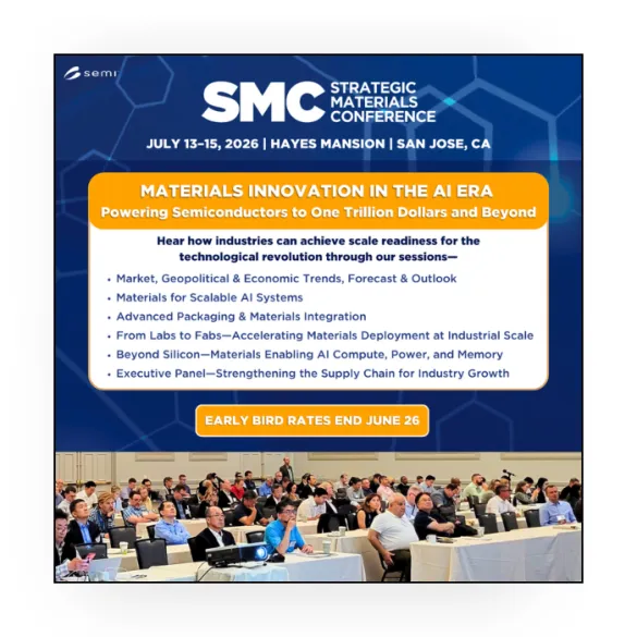
Materials Innovation in the AI Era: Powering Semiconductors to One Trillion Dollars and Beyond
Beyond the AI boom lies a challenge—and opportunity—that is far more foundational: ensuring the materials ecosystem underpinning a $2.5 trillion industry is resilient enough to support the next era of innovation. As artificial intelligence accelerates demand for advanced hardware, energy infrastructure, and high‑performance components, the pressure on global materials supply chains has never been greater.
This year, SMC explores how industries can achieve scale readiness through smarter design, diversified sourcing, sustainable processes, and breakthrough materials science. It invites leaders to look past the excitement of AI itself and toward the essential building blocks that will determine whether this technological revolution is secure and sustainable.
Sessions
Market, Geopolitics & Outlook
Materials for Scalable AI Systems
Advanced Packaging & Materials Integration
From Labs to Fabs—Accelerating Materials Deployment at Industrial Scale
Quantum & Emerging Devices
Executive Panel–Strengthening the Supply Chain
REGISTRATION INCLUDES
Approved speaker PDF presentations
Breakfast, lunch, coffee breaks
Two networking receptions
Tabletop exhibits
WHO SHOULD ATTEND
SMC offers valuable content and unprecedented networking opportunities for semiconductor industry professionals who share common strategic objectives on materials innovation, management, and business success.
CEO ● CTO ● Presidents & General Managers ● Executive VP & Senior Executives ● Engineering & Fab Managers ● Academia ● Startup Founders ● Financial Analysts ● Market Researchers ● Consulting Firms ● Consortiums
Off
Add to Calendar2026-07-13 00:00:002026-07-15 00:00:00SMC 2026—Strategic Materials Conference Hayes Mansion 200 Edenvale Avenue San Jose, CA, CA 95136 United StatesSEMI.org[email protected]America/Los_Angelespublic
America/Los_Angeles
1
Rapid advances in electronics, sensors, computation, wireless systems, artificial intelligence, and neurotechnology are creating a new generation of medical solutions that interact directly with the body’s electrical and physiological control systems. Collectively described as bioelectronic medicine, these technologies offer the potential to complement—and in some applications overcome important limitations of—traditional pharmaceutical approaches by providing interventions that can be spatially targeted, dynamically adjusted, continuously monitored, and personalized to an individual patient’s physiology.
This Master Class will provide a broad introduction to the rapidly evolving field of bioelectronic medicine from the perspective of electrical and computer engineering. It will examine how technologies familiar to engineers—including low-noise sensing, embedded computing, signal processing, machine learning, wireless communications, miniaturized stimulation electronics, wearable devices, and closed-loop control—are being translated into new diagnostic and therapeutic platforms. Examples will range from cardiac pacemakers and cochlear implants to deep-brain stimulation, vagus nerve stimulation, spinal cord stimulation, transcranial stimulation, peripheral nerve interfaces, and digital biomarkers. Particular attention will be given to the transition from open-loop stimulation toward sensor-guided, closed-loop bioelectronic medicine, in which physiological measurements provide real-time feedback for optimizing stimulation parameters and tracking therapeutic responses. The Master Class will also explore why engineers are increasingly central to the future of medicine. Biological systems present unusual engineering challenges: signals are weak and noisy, anatomy and physiology vary substantially between individuals, neural systems are nonlinear and adaptive, and successful devices must operate safely at the interface between electronics and living tissue. These challenges are generating opportunities for innovation across semiconductor technology, MEMS and wearable sensors, electrode design, power management, computational modeling, AI, cybersecurity, human-machine interfaces, and systems engineering.
The Master Class will conclude with a look toward the next generation of bioelectronic medicine: intelligent therapeutic systems and digital twins capable not simply of measuring disease or delivering predetermined stimulation, but of continuously sensing physiological state, interpreting changes in biological function, and adapting interventions to promote recovery and maintain health. For electrical and computer engineers, this emerging field represents an opportunity to apply core engineering disciplines to some of the most consequential challenges in human health.
ABOUT THE SPEAKER
John Ralston, PhD, CEO and Co-founder, Neursantys Inc. John Ralston is a pioneer in the development of non-invasive bioelectronic devices and adaptive neuroplastic treatments for neurosensory, neuromotor, and neurocognitive impairments that have limited pharmacological treatment options.
At Neursantys, John is collaborating with healthcare researchers, providers, and payers to restore motor and cognitive functions that have been impaired by both normal aging and accelerated aging caused by head trauma, disease, and spaceflight.
With a career spanning public and private R&D organizations and entrepreneurial ventures in Canada, Europe, and the U.S., John has authored/co-authored over 250 professional publications, presented over 150 talks and seminars, and has 16 issued patents. John earned B.Sc. degrees in Physics and Electrical Engineering from M.I.T., a PhD in Electrical Engineering from Cornell University, and the MSc in Management of Technology from the MIT Sloan School of Management.
Join Dr. John Ralston, Founder and CEO of Neursantys, a pioneering bioelectronics company developing non-invasive neurostimulation and wearable technologies for diagnosing and treating neuromotor conditions, for an engaging Master Class on the rapidly advancing field of bioelectronic medicine.
Learn how innovations in sensors, AI, embedded systems, neural interfaces, and closed-loop therapies are enabling personalized, real-time treatments that interact directly with the body’s physiological systems and are shaping the future of healthcare.
Recent Advances in Bioelectronics Medicine
Flexible Electronics Master Class #32
10:00 am - 12:00 pm
Off
Add to Calendar2026-11-18 10:00:002026-11-18 12:00:00FEMC#32 Recent Advances in Bioelectronics MedicineJoin Dr. John Ralston, Founder and CEO of Neursantys, a pioneering bioelectronics company developing non-invasive neurostimulation and wearable technologies for diagnosing and treating neuromotor conditions, for an engaging Master Class on the rapidly advancing field of bioelectronic medicine. Learn how innovations in sensors, AI, embedded systems, neural interfaces, and closed-loop therapies are enabling personalized, real-time treatments that interact directly with the body’s physiological systems and are shaping the future of healthcare.United StatesSEMI.org[email protected]America/Los_Angelespublic
America/Los_Angeles
Register Here
Leverage SEMI U learning opportunities to accelerate your professional development in 2027. Our commitment remains focused on delivering comprehensive technical education that helps you build the knowledge and skills needed to thrive in the semiconductor industry.
Join us for our upcoming, "Kickstart 2027 with SEMI University," where you'll get an exclusive preview of new learning opportunities, upcoming training events, and special savings available to learners.
During this webinar, you will:
Discover the latest updates and enhancements to SEMI U's on-demand course catalog.
Explore upcoming virtual and in-person instructor-led training programs scheduled for the first half of 2027.
Learn how to maximize your professional development with SEMI U resources and learning pathways.
Receive access to a special 10% discount on all on-demand courses.
Don't miss this opportunity to plan your learning journey and stay ahead in a rapidly evolving industry. Register today to reserve your spot.
Join us to explore SEMI U's current course offerings and upcoming virtual and in-person training opportunities designed to support your professional growth in the semiconductor industry. You'll also have the chance to engage directly with our team during a live Q&A session. As a thank you for attending this free webinar, you'll receive:
A 10% discount code valid on all SEMI U on-demand courses.
Entry into a raffle to win a complimentary course bundle valued at $100.
Kickstart 2027 with SEMI University - ASIA
Webinar (PM session)
January 28, 2027
9:00 am - 9:30 am
Off
Add to Calendar2027-01-28 09:00:002027-01-28 09:30:00Kickstart 2027 with SEMI University - ASIAJoin us to explore SEMI U's current course offerings and upcoming virtual and in-person training opportunities designed to support your professional growth in the semiconductor industry. You'll also have the chance to engage directly with our team during a live Q&A session. As a thank you for attending this free webinar, you'll receive:A 10% discount code valid on all SEMI U on-demand courses. Entry into a raffle to win a complimentary course bundle valued at $100. United StatesSEMI.org[email protected]Asia/Singaporepublic
Asia/Singapore
Leverage SEMI U learning opportunities to accelerate your professional development in 2027. Our commitment remains focused on delivering comprehensive technical education that helps you build the knowledge and skills needed to thrive in the semiconductor industry.
Join us for our upcoming, "Kickstart 2027 with SEMI University," where you'll get an exclusive preview of new learning opportunities, upcoming training events, and special savings available to learners.
During this webinar, you will:
Discover the latest updates and enhancements to SEMI U's on-demand course catalog.
Explore upcoming virtual and in-person instructor-led training programs scheduled for the first half of 2027.
Learn how to maximize your professional development with SEMI U resources and learning pathways.
Receive access to a special 10% discount on all on-demand courses.
Don't miss this opportunity to plan your learning journey and stay ahead in a rapidly evolving industry. Register today to reserve your spot.
Join us to explore SEMI U's current course offerings and upcoming virtual and in-person training opportunities designed to support your professional growth in the semiconductor industry. You'll also have the chance to engage directly with our team during a live Q&A session. As a thank you for attending this free webinar, you'll receive:
A 10% discount code valid on all SEMI U on-demand courses.
Entry into a raffle to win a complimentary course bundle valued at $100.
Kickstart 2027 with SEMI University - US/EU
Webinar (AM session)
January 27, 2027
8:00 am - 8:30 am
Off
Add to Calendar2027-01-27 08:00:002027-01-27 08:30:00Kickstart 2027 with SEMI University - US/EU Join us to explore SEMI U's current course offerings and upcoming virtual and in-person training opportunities designed to support your professional growth in the semiconductor industry. You'll also have the chance to engage directly with our team during a live Q&A session. As a thank you for attending this free webinar, you'll receive:A 10% discount code valid on all SEMI U on-demand courses. Entry into a raffle to win a complimentary course bundle valued at $100. United StatesSEMI.org[email protected]America/Los_Angelespublic
The workshop will focus on recent advances in analytical methods and instrumentation that address near-term particle metrology challenges identified in the 2024 IRDS Roadmap.
Near-Term Metrology Challenges
Challenge
Description
#5 — Slurry Particle Characterization
Insufficient metrology capability and other impurity monitoring.
Need reliable LPC metrology that can measure targeted particle sizes and concentrations that ignore MPS sizes and do not require sample dilution to obtain the measurement.
#9 — Post-CMP (pCMP) Cleans Particles
Some pCMP cleans have volatile or highly reactive ingredients that form bubbles, requiring new metrology to differentiate bubbles from real particles. Cleans containing surfactants form micelle particles that must be distinguished from foreign particles.
#16 — Particle Precursor Metrology < 10nm
Need better understanding of particle precursors and critical concentrations to form particles, and the relationship between species/concentration and particle size.
Moscone Center South Hall, Level 3, Room 314 San Francisco, CA United States
8:30 am - 12:15 pm
Off
Add to Calendar2026-10-14 08:30:002026-10-14 12:15:00SEMI Liquid Chemicals Analytical ForumSEMI StandardsLiquid Chemicals Analytical ForumMoscone Center South Hall, Level 3, Room 314 San Francisco, CA United StatesSEMI.org[email protected]America/Los_Angelespublic
Contact
For any questions about the event, please contact:
Laura Nguyen Sr. Coordinator, International Standards
Subhadra Sampathkumaran, M.S. in Computer Science, is a Software Engineering Manager at Intel Corporation with over 20 years of experience leading digital transformation, data engineering, and automation across global semiconductor fabs. She has built and scaled solutions spanning software architecture, advanced analytics, manufacturing operations, big
data integration, IoT, workflow automation, and agentic AI, helping improve efficiency, reduce costs, enhance operational resilience, strengthen compliance, and enable predictive maintenance, lights-out manufacturing, and real-time decision support. Passionate about orchestrating intelligence across facilities and sub-fabs, she envisions a future where maintenance and operations evolve from reactive, time-based models into adaptive, anticipatory ecosystems that redefine reliability engineering.
Sean Tropsa
Sean Tropsa began his career as an engineer in the semiconductor manufacturing industry, where he developed expertise in large-scale data analysis, root cause analysis, and process optimization. As Head of Technical Solutions, Growth Markets at Seeq, he helps semiconductor customers use analytics and AI to turn data into business value, supporting sustainability goals while improving reliability, yield, and quality. Sean earned BS and MS degrees in Chemical Engineering from Arizona State University.
United States
Learn how Intel is using agentic AI-supported workflows in Seeq to transform maintenance operations across its global semiconductor manufacturing footprint. With thousands of critical assets across multiple sites, Intel is projecting 30% faster anomaly detection in ultrapure water systems, a 15-20% reduction in technician workload through autonomous work order generation, and more than 120,000 labor hours saved annually.
These results are powered by a shift from time-based and alarm-driven maintenance to condition-based operations. Intel leverages Seeq to continuously monitor asset health, detect abnormal conditions earlier, forecast maintenance needs, generate work orders, and provide engineers with actionable context. By codifying the expertise of its global engineering and operations teams into scalable workflows, Intel is extending institutional knowledge across facilities, improving consistency, and accelerating action. With human oversight built into every step, Intel is on a practical, governed journey toward semi-autonomous maintenance operations.
This session will explore real-world applications in ultrapure water and compressor maintenance and share practical lessons for implementing agentic AI at scale, including governance, repeatability, and scaling AI-driven reliability programs across a global manufacturing enterprise.
Scaling Smarter Maintenance in Semiconductor Facilities with AI Agents
9:00 am - 10:00 am
Off
Add to Calendar2026-09-29 09:00:002026-09-29 10:00:00Scaling Smarter Maintenance in Semiconductor Facilities with AI AgentsLearn how Intel is using agentic AI-supported workflows in Seeq to transform maintenance operations across its global semiconductor manufacturing footprint. With thousands of critical assets across multiple sites, Intel is projecting 30% faster anomaly detection in ultrapure water systems, a 15-20% reduction in technician workload through autonomous work order generation, and more than 120,000 labor hours saved annually.These results are powered by a shift from time-based and alarm-driven maintenance to condition-based operations. Intel leverages Seeq to continuously monitor asset health, detect abnormal conditions earlier, forecast maintenance needs, generate work orders, and provide engineers with actionable context. By codifying the expertise of its global engineering and operations teams into scalable workflows, Intel is extending institutional knowledge across facilities, improving consistency, and accelerating action. With human oversight built into every step, Intel is on a practical, governed journey toward semi-autonomous maintenance operations.This session will explore real-world applications in ultrapure water and compressor maintenance and share practical lessons for implementing agentic AI at scale, including governance, repeatability, and scaling AI-driven reliability programs across a global manufacturing enterprise.United StatesSEMI.org[email protected]America/Los_Angelespublic
America/Los_Angeles
Register
High-temperature materials are critical for applications in harsh-environment circuitry, where devices must operate reliably under extreme thermal, chemical, and mechanical stress. In this Master Class, Dr. Shenqiang (Shen) Ren will present a high-throughput ink materials development strategy enabled by non-equilibrium processing and hybrid additive manufacturing. This approach enables rapid synthesis, combinatorial screening, and direct integration of functional materials onto diverse substrates. The resulting materials exhibit strong electrical performance, robust adhesion, and long-term stability under harsh operating conditions. This high-throughput framework accelerates the discovery and deployment of printable materials for interconnects, heaters, and EMI shielding, providing a versatile pathway toward next-generation printed electronics designed for extreme environments.
ABOUT THE SPEAKER
Shenqiang (Shen) Ren, PhD Dr. Shenqiang Ren is a Professor of Materials Science and Engineering at the University of Maryland, College Park, with research interests in emerging functional and structural materials. He received his Ph.D. in Materials Science and Engineering from the University of Maryland, College Park, and subsequently completed postdoctoral training at the Massachusetts Institute of Technology (MIT).
United States
Shenqiang (Shen) Ren , PhD
Department of Materials Science and Engineering, Professor
Join us for a focused Master Class with Dr. Shenqiang (Shen) Ren, exploring the development of high‑temperature materials for harsh‑environment printed and flexible hybrid electronics (FHE). This session will examine how devices can be engineered to operate reliably under extreme thermal, chemical, and mechanical stress—conditions where conventional materials and processes often fail.
The Master Class will also highlight how this high‑throughput framework accelerates the discovery and deployment of printable materials for interconnects, heaters, and EMI shielding, offering a versatile pathway toward next‑generation printed electronics designed for extreme conditions.
High Throughput Material Development for Extreme Environment Printed Electronics
Flexible Electronics Master Class #30
10:00 am - 12:00 pm
Off
Add to Calendar2026-08-26 10:00:002026-08-26 12:00:00FEMC#30 High Throughput Material Development for Extreme Environment Printed ElectronicsJoin us for a focused Master Class with Dr. Shenqiang (Shen) Ren, exploring the development of high‑temperature materials for harsh‑environment printed and flexible hybrid electronics (FHE). This session will examine how devices can be engineered to operate reliably under extreme thermal, chemical, and mechanical stress—conditions where conventional materials and processes often fail.The Master Class will also highlight how this high‑throughput framework accelerates the discovery and deployment of printable materials for interconnects, heaters, and EMI shielding, offering a versatile pathway toward next‑generation printed electronics designed for extreme conditions.United StatesSEMI.org[email protected]America/Los_Angelespublic
America/Los_Angeles
watch on-demand
※ Group registration fee applies to groups of five or more from the same company. ※ For group registration inquiries, please contact SEMI Korea Program Team at [email protected].
Making 3DIC Manufacturable for AI: From Vertical Integration to Scalable Production
As AI systems push requirements for higher bandwidth, lower power, and increased integration density, 3D integrated circuits (3DIC) are moving rapidly from development to production. However, scaling 3DIC introduces complex application challenges across the manufacturing flow, where process interactions and control become critical.
This talk examines key 3DIC applications and process challenges, including high aspect ratio TSV etch, void free TSV fill, and dielectric deposition, required for reliable wafer and die level stacking. Emerging applications such as inter die gap fill for advanced chiplets integration and plasma dicing for improved yield, edge quality, and die strength further increase integration complexity and productivity demands.
The presentation highlights Lam Research innovations across etch, deposition and clean processes that enable tighter process windows, improved uniformity, and higher throughput. In addition, equipment intelligence and data driven control are increasingly essential to enhance yield learning and manufacturing productivity. Together, these advances are enabling scalable, high volume 3DIC manufacturing for next generation AI systems.
The future of compute will not be defined by silicon alone. As AI reshapes industries and economies, advanced packaging has become the foundation of the next era of innovation, enabling unprecedented gains in performance, efficiency, and scale. During his keynote, Yin Chang will explore how breakthroughs in heterogeneous integration, chiplets, and advanced manufacturing are transforming bold AI ambitions into deployable systems, and why AI leadership will depend not only on compute power, but on the ability to integrate and manufacture at scale.
The rapid electrification of automotive and industrial systems is placing increasingly stringent demands on power semiconductor devices in terms of voltage capability, thermal performance, reliability, and system integration. This presentation reviews recent trends in power devices and power module packaging technologies aimed at improving performance while addressing cost and manufacturability constraints.
First, the fundamental differences between digital and power devices are outlined, followed by an overview of power device applications based on silicon (Si), silicon carbide (SiC), and gallium nitride (GaN) technologies, together with Amkor’s product portfolio.
Next, power module packaging technologies are discussed with a focus on key electrical and thermal challenges. Representative solutions, including advanced interconnects, cooling architectures, and embedded power modules, are introduced, along with a brief overview of Amkor’s technology roadmap.
Finally, the role of the Amkor Technology Japan R&D Center in supporting open innovation and global collaboration is briefly discussed.
The presentation explores advanced packaging technologies designed to meet the escalating performance and power efficiency demands of AI and High-Performance Computing (HPC). To overcome the limitations of traditional semiconductor architectures, System Technology Co-Optimization (STCO) is introduced as a critical framework for managing thermal crosstalk and enhancing heterogeneous integration. The discussion highlights key innovations, including Customized HBM (cHBM) for optimized base-die performance and Samsung's 2.xD packaging portfolio, which encompasses Cube S, Cube E, and Cube R. Specifically, the 2.3D Cube E leverages panel level packaging to enable larger interposers and increased HBM integration, significantly improving productivity and reducing silicon fab burdens. The technical achievements in PLP—such as precise warpage control and the realization of fine RDL patterns (2/2μm)—are detailed to demonstrate their viability for large-scale AI chips. Furthermore, the roadmap extends toward 3D integration and Co-Packaged Optics (CPO) to maximize bandwidth and energy efficiency. Finally, the importance of an ecosystem-wide collaboration is emphasized as the driver for future innovation in "More than Moore" technology. These advancements collectively provide a scalable path toward the next generation of AI hardware acceleration.
Corporate Officer, GM(General Manager) of R&D Div.
SHINKO ELECTRIC INDUSTRIES
Latest Development Status of Glass Core Build-up Substrate
Glass core substrates exhibit low CTE and significantly higher rigidity than conventional organic substrates and are therefore regarded as promising core materials for next-generation build-up packages. However, a major challenge lies in the occurrence of SeWaRe defects (delamination in glass), which arise from thermal stresses induced by the mismatch in the coefficients of thermal expansion (CTE) between the glass material and the build-up resin.
To mitigate this issue, we proposed a structure in which the corner regions of each individual piece are formed from resin. However, considering the thermal history during chip mounting, it became evident that the suppression effect was insufficient. Therefore, an edge‑protection material was applied to relieve the stress concentrated at the edges of each individual piece. As a result, it was confirmed that SeWaRe defects could be effectively suppressed even under thermal loading.
Through these efforts, we successfully developed a glass core build-up package substrate incorporating 11 layers of single‑sided copper wiring (22 layers in total).
Beyond Moore's Law: How Silicon Photonics and Advanced Packaging Are Redefining HPC
AI and data-intensive workloads are outpacing what conventional semiconductor technology can deliver. Two innovations are stepping in to close the gap: Silicon Photonics, which brings optical-speed, low-power data transmission into the data center, and Advanced Packaging, which uses chiplets and 2.5D/3D integration to maximize performance and efficiency at the chip level.
This talk examines how these complementary technologies are reshaping HPC architecture—covering their current state, how they work in tandem, and the key technical and commercial barriers to large-scale adoption.
Co-packaged optics (CPO) is emerging as a key enabler for scaling bandwidth while containing power and cost in next-generation AI and cloud infrastructure. By moving optical engines closer to the switch ASIC and shortening high-speed electrical reaches, CPO can reduce SerDes power, ease signal-integrity constraints, and increase overall front-panel bandwidth density. However, delivering these benefits at volume requires new approaches across package architecture, manufacturing, and system integration.
This presentation reviews the main packaging challenges that must be solved to industrialize CPO, including thermal management and heat spreading near high-power silicon, fiber attach and optical alignment tolerances, photonics/laser integration choices, high-density optical and electrical I/O, substrate and interposer selection, and reliability risks such as warpage, CTE mismatch, and contamination control. Test and rework strategy, yield learning, and supply-chain readiness (materials, assembly, and metrology) are highlighted as practical barriers to adoption.
The talk also outlines opportunities created by CPO packaging innovations—such as modular optical tiles, standardized fiber interfaces, advanced lid/heat-sink concepts, and co-design of electrical, mechanical, and optical domains—to unlock higher radix switches and lower system power. Attendees will leave with a structured view of technology tradeoffs, a roadmap of near-term versus long-term packaging options, and actionable considerations for bringing CPO from prototypes to deployable products.
Advanced Packaging Summit 2026, under the theme “Packaging the Future of AI – From Silicon to Photon,” will examine the evolution of packaging technologies in the AI era and their broader implications for the semiconductor industry. Featuring presentations by leading industry experts, the summit will explore market shifts driven by the growing demand for AI semiconductors, along with key technologies enabling advanced packaging. The program will also highlight the innovation journey from silicon-based integration technologies to photonics-based interconnects, which are essential to enhancing packaging productivity and scalability. Panel discussions in each session will further provide opportunities to exchange insights on real-world applications, technical challenges, and possibilities for cross-industry collaboration, while exploring new business opportunities and strategic perspectives created by advanced packaging technologies in the AI era.
ADVANCED PACKAGING SUMMIT 2026
July 15(Wed), 2026 | Convention Hall 1, 3F, Suwon Convention Center
8:30 am - 5:00 pm
Off
Add to Calendar2026-07-15 08:30:002026-07-15 17:00:00ADVANCED PACKAGING SUMMIT 2026Advanced Packaging Summit 2026, under the theme “Packaging the Future of AI – From Silicon to Photon,” will examine the evolution of packaging technologies in the AI era and their broader implications for the semiconductor industry. Featuring presentations by leading industry experts, the summit will explore market shifts driven by the growing demand for AI semiconductors, along with key technologies enabling advanced packaging. The program will also highlight the innovation journey from silicon-based integration technologies to photonics-based interconnects, which are essential to enhancing packaging productivity and scalability. Panel discussions in each session will further provide opportunities to exchange insights on real-world applications, technical challenges, and possibilities for cross-industry collaboration, while exploring new business opportunities and strategic perspectives created by advanced packaging technologies in the AI era.Convention Hall 1, 3F, Suwon Convention Center South Korea South KoreaSEMI.org[email protected]Asia/Seoulpublic
Asia/Seoul
Setting the Stage: Industry Drivers & SCC Initiative Context
• Semiconductor Industry Decarbonization Challenges
• The Need for Quantified Business Cases
• SCC Initiative Background & Development Journey
• Vision for Industry Adoption & Collaboration
• Tool Architecture & Methodology
• Key Inputs & Assumptions
• Understanding the Outputs & Metrics
• Live Demonstration & Example Scenario
• Current Limitations & Future Development Opportunities
9:36 am
-
9:50 am
Jeff Rudnik
Director of Environmental Sustainability & Net Zero
ASM
Industry Use Cases & Practical Applications
• Evaluating Decarbonization Projects
• Comparing Alternative Mitigation Strategies
• Supporting Internal Investment Decisions
• Lessons Learned from Early Applications
• Opportunities for Industry Collaboration
The semiconductor industry is under increasing pressure to decarbonize its operations, particularly with regard to Scope 1 emissions — direct greenhouse gas emissions (GHG) from owned or controlled sources. Yet many companies face a persistent challenge: how to make a clear, consistent, and financially credible case for emissions reduction investments. To help address this need, the Semiconductor Climate Consortium (SCC) has developed a Cost-Benefit Calculator — a simplified and flexible tool that offers a structured starting point for evaluating carbon emissions reduction projects. The calculator enables users to estimate the Net Present Cost (NPC) per ton of CO₂ equivalent emissions reduction, helping to translate environmental impact into business-relevant terms.
Join SEMI's Semiconductor Climate Consortium (SCC) Scope 1 Working Group and document authors for a webinar discussing their journey creating the Cost-Benefit Calculator and outlining the use cases for this tool. The Cost-Benefit Calculator is a functional spreadsheet with built in report creation tools. For business managers who need to calculate emissions for Scope 1.
Building the business case for emission reductions
9:00 am - 10:00 am
Off
Add to Calendar2026-06-16 09:00:002026-06-16 10:00:00SCC: Cost Benefit Calculator WebinarThe semiconductor industry is under increasing pressure to decarbonize its operations, particularly with regard to Scope 1 emissions — direct greenhouse gas emissions (GHG) from owned or controlled sources. Yet many companies face a persistent challenge: how to make a clear, consistent, and financially credible case for emissions reduction investments. To help address this need, the Semiconductor Climate Consortium (SCC) has developed a Cost-Benefit Calculator — a simplified and flexible tool that offers a structured starting point for evaluating carbon emissions reduction projects. The calculator enables users to estimate the Net Present Cost (NPC) per ton of CO₂ equivalent emissions reduction, helping to translate environmental impact into business-relevant terms.Join SEMI's Semiconductor Climate Consortium (SCC) Scope 1 Working Group and document authors for a webinar discussing their journey creating the Cost-Benefit Calculator and outlining the use cases for this tool. The Cost-Benefit Calculator is a functional spreadsheet with built in report creation tools. For business managers who need to calculate emissions for Scope 1.SCC members can download the Cost Benefit Calculator Report here.SEMI United StatesSEMI.org[email protected]America/Los_Angelespublic
America/Los_Angeles
Register Today!