downloadGroupGroupnoun_press release_995423_000000 copyGroupnoun_Feed_96767_000000Group 19noun_pictures_1817522_000000Member company iconResource item iconStore item iconGroup 19Group 19noun_Photo_2085192_000000 Copynoun_presentation_2096081_000000Group 19Group Copy 7noun_webinar_692730_000000Path
Skip to main content
Default Banner Image

Technology and Trends

This article is the fourth in a series highlighting the vital importance of SEMI Standards to commemorate the publication of the 1000th SEMI Standard in July 2019. Find the entire series here.Computer prices have plunged over the years even as desktop and laptop PC performance has skyrocketed thanks to the semiconductor industry, giving users much more bang for their buck. The chip industry stands in a stark contrast to healthcare and education with their exponentially rising costs.What distinguishes the semiconductor industry from healthcare and education in the capacity to deliver so much for so much less over time? After all, even in other parts of the technology sector that are heavily regulated, such as cable television, we have not witnessed the same price decreases as in microelectronics.Some pundits claim that the difference among sectors is tied to their degree of regulation. Does greater regulation somehow degrade product value? The reality is far more nuanced. But one thing is clear: Smart self-regulation (i.e. standards) in the semiconductor industry has contributed mightily to its success.The recipe for success has been simple. Standards have been rocket fuel for competition, which in turn has sparked innovation, driving down device prices while boosting performance. Computer prices fell dramatically between 1997-2015 while the cost of cable TV and internet services rose. Myth of unregulated competitionA semiconductor fab might actually be the most regulated place on earth. Fabs hew to a much higher standard of air quality and cleanliness than even uber-sterile hospital operating rooms. Manufacturing processes are voluntarily regulated not to millimeters, but to nanometers. While some standards are proprietary with limited reach, others span the supply chain. Regulation has worked so well in this sector that the semiconductor industry isn’t moving toward less standardization. It’s moving toward more. Secret is smart standards The gap between regulation and self-regulation is more like a chasm. We typically view regulation as a series of top-down directives that more often focus on the interests of the producer than the consumer. Healthcare regulation, for example, may improve quality of care, but it’s often insurers, big pharma and hospitals that benefit most from regulation, rather than consumers.The semiconductor industry, on the other hand, uses self-regulation to improve business operations and make better products for consumers. Falling prices and rising performance are natural byproducts.Semiconductor industry self-regulation is an ecosystem-wide effort, where input isn’t just top-down, but also bottom-up or even side-to-side. The first SEMI Standard, which specified wafer sizes, exemplifies this approach.The SEMI Standards Committee formed in 1973 to address silicon wafer dimensional specifications. At the time, wafer specifications proliferated. Numbering more than 2,000, the various specifications led to major inefficiencies just when the industry was just getting underway. Wafer suppliers banded together under SEMI to solve this problem and rapidly developed consensus specifications for 2- and 3-inch wafers. By the mid-1970s, over 80% of wafers conformed to these new standards.Standardized wafer sizes freed equipment companies to focus on innovations that reduced cost and increased performance. It also allowed manufacturers to focus on product differentiation without having to worry about device fabrication process and cost. Since that first SEMI Standard made possible the modern semiconductor equipment industry, original equipment manufacturers (OEMs) have competed to deliver amazing innovations. For example, lithography systems routinely use light to design chips with feature sizes smaller than the wavelength of light.SEMI’s 1000th standard on energetic materials demonstrates how smart standards are also pragmatic. This standard is not about banning materials or assigning blame when things go awry. It is about creating practical guidelines that companies will follow, enabling them to realize greater innovation. Guidelines that reduce accidents and risks will spur more, not less, energetic materials’ exploration. Industry suppliers will be the big winners.The 1st to the 1000th SEMI standard all represent examples of cooperation making more sense than competition.Standards for the real worldCreating a business-friendly standard that still gets the job done is a process. As SEMI Standards Task Force and Committee members, materials, equipment and manufacturing companies take part in defining best practice guidelines that support safe and practical use of materials and equipment. Task force and committee members assign particular responsibilities and associated costs to the most logical segments of the supply chain. They also develop information-sharing practices around competitive process recipes and purity standards.Andy McIntyre, CIH, a member of the energetic materials task force and an executive vice president and managing principal at BSI EHS Services and Solutions, summarized what makes SEMI standards smart.“SEMI standards are pragmatic,” said McIntyre. “They take into account the need for implementation in a real-world business environment. They embrace an engineering approach to problem-solving to create practical solutions, and they define specifications and performance goals in ways that allow engineers — in collaboration with EHS professionals — to identify practical solutions for reducing risk in R D, pilot line and manufacturing operations.“SEMI standards employ a holistic process that considers all the important points of view throughout the supply chain, from materials selection, installation, use, recycling and/or disposal,” said McIntyre. “The breadth of SEMI EHS Guidelines, for example, is also very comprehensive as the SEMI EHS Committee and task forces work to ensure that standards keep pace with dynamic technology developments. Energetic materials is a prime example where the industry recognized the need for a new safety guideline to document safe usage of pyrophoric, water-reactive and unstable reactive materials, which have become increasingly important in semiconductor and advanced materials R D and manufacturing.”This is the real secret to the success of the semiconductor industry. Smart self-regulation allows industry players to cooperate in the development and implementation of standards that are pragmatic, comprehensive and dynamic. Participants in SEMI Standards have a voice in the semiconductor industry because they are the voice of the semiconductor industry.While innovation in semiconductors may not always keep pace with Moore’s Law, we can depend on one truth: As long as collaboration and cooperation are the rule and not the exception, we will continue to advance technology in amazing and unprecedented ways. You, me and all other consumers will continue to reap the rewards of innovation. Use your voice to affect standardization in and around the semiconductor industry. Learn about SEMI Standards – and become part of the solution.Heidi Hoffman is senior director of technology communities marketing at SEMI. Hoffman and her team shine a spotlight on the work of the more than 20 technology communities under the SEMI electronics manufacturing supply chain collaboration platform. Actively engaging community members in marketing programs that showcase their unique value, Hoffman’s team helps companies to grow and prosper through the power of connection, collaboration and innovation.
Read More
ASN had a chance to talk to François Brunier of Soitec, who’s leading this important project.Advanced Substrate News (ASN): Can you tell us briefly about OCEAN12?Francois Brunier (FB): OCEAN12 stands for Opportunity to Carry European Autonomous driviNg further with FD-SOI technology up to the 12nm node.Francois Brunier, Partnership Program Manager, Soitec.OCEAN12 deals with “Ultra-low power computing solutions for automotive and aeronautics using all the range of FDSOI technologies”. This project with a budget of 103M€ brings together 27 partners from 7 different countries. The project received the ECSEL JU* label under the 2017 call. ECSEL is an EU-driven public-private partnership enabling the co-financing of innovation in electronic components and systems both by Member States and the European Union.ASN: Why is this project needed?FB: As of today a car has around 500 million transistors. These electronic components represent already an important vector of valorization and differentiation for the automotive industry and for the consumer. The increased autonomy of the vehicles will require a very strong build-up of computational capacities. 50 to 100 times more transistors could be required for a level 5 (fully autonomous car). Following this trend an autonomous car will require power consumption equivalent to 50 to 100 computers running continuously (without taking into account the car propulsion).The OCEAN12 partners.The power consumption of these components becomes a key element in the choice of technologies. We believe that our technologies on SOI present the best assets to meet this challenge.The FD-SOI substrates, technologies and designs developed in OCEAN12 offer a palate of different solutions to this challenge: increased performance for data processing (including Artificial Intelligence); much higher energetic efficiency; and smaller form factors to fit in embedded systems like autonomous cars with higher integration and reliability, and enabling safe connectivity.The OCEAN12 project will demonstrate that SOI technologies are able to meet these challenges through relevant demonstrators in the targeted fields.ASN: What are the project goals?FB: OCEAN12 will bring concrete solutions to the main challenges of smart connectivity and low power consumption in the automotive industry.As such, OCEAN12 will build awareness around the key enabling technologies in substrate development, transistor behavior, and the design and fabrication of integrated circuits up to the system and end-user application levels. We will show that the technology is advantageous for automotive and aerospace applications, which are strategic sectors for Europe. Having the whole supply chain in Europe means having trusted and secured components made in Europe.The OCEAN12 project goals stand on three pillars:First: Confirming the technology foundation. Ocean12 puts the FD-SOI substrate and device developers in direct contact with the full value chain of suppliers and end users. This gives the entire ecosystem visibility into current and future needs, and ensures that substrate and device solutions are both technically feasible and correctly aligned with actual system requirements.Second: Creating concrete, innovative demonstrators in automotive (Audi, Bosch) and aeronautics (Airbus, Thales). These demonstrators are a first step in defining the context and environment to prove the advantages of these technologies in real application cases, showing they are useful and as such prefigure a final system and a potential future product roadmap. Demonstrators should be as close as possible to the final application.Third: Broadening the design ecosystem, with the big companies, the small- and medium-sized companies (SMEs) and the research organizations (universities, RTOs). We have a critical mass of 16 design ecosystem partners focusing their efforts on FD-SOI. The project leverages that dynamic FD-SOI design ecosystem for IC product migration to FD-SOI and the creation of new IP. Inventing the future components in Europe is also key.ASN: Can you tell us more about the demonstrators? When will we see them?FB: There are four demonstrators. All these demonstrators will be delivered by the end of the project in 2021:Always-on wake-up systems (Audi, Bosch, Leti). With such a system we can imagine an application to monitor our car when it is parked in a parking lot for a long time. The sensors would remain aware of everything that goes on around the car. Based on sensor observations, the car can make decisions on further actions to take. This can be used in many future car applications like intrusion detection or vehicle access systems. But you will not have to worry about battery drain: even though all the sensors are always on, they go right back into a very low-power sleep mode thanks to FD-SOI technology.mm-Wave integrated radar SOCs (Bosch and Audi), which will benefit from all the innovations of FD-SOI thanks to its low consumption properties, but also the optimization of the sensors. The performance gain is made over the entire system with adaptations between analog and logic.High-performance video processor for aeronautics. (Airbus, Thales, Kalray). Kalray, a French SME working on Massively Parallel Processor Arrays (MPPA) aims to demonstrate an ultra-low power, low-cost, high-performance neural processor on FD-SOI technology. This demonstrator would be key for Airbus and drones with high-performance, low-power cameras. Airbus and Audi have partnered on air and ground mobility services.Microcontroller plug-and-play board. This demonstrator lead by ST will allow for the development of new solutions in the domain of GNSS/GPS.ASN: Can you tell us more about the partners?FB: The OCEAN12 consortium of 27 partners involves 8 large groups, 9 SMEs and 10 universities/RTOs. These partners come from 7 different European countries.The eight large groups include: Soitec, the world’s leading provider of FD-SOI substrates; EVG, a leading global equipment supplier; GlobalFoundries and STMicroelectronics, the two major European FD-SOI foundries; and Bosch, as a Tier 1 automotive supplier. At the top of the value chain, high-end European automotive manufacturer Audi, the avionics industrial giant Airbus, and Thales for security issues, will develop product demonstrations.Ten highest-level research institutes support the industrial consortium. They include CEA-Leti (FR), Fraunhofer(GE), IMS (FR), INP Grenoble (FR), TU Dresden (GE), U. Paderborn (GE), Bundeswehr U. Munich (GE), Eberhard Karls U. Tübingen (GE), Instituto de Telecomunicações (PT), and Warsaw UT (PL). They increase the competitiveness through technological innovation and transfer of technical know-how while gaining new expertise working with global leaders.In addition, OCEAN 12 has a very strong SME consortium covering the supply chain in the fields of new equipment, IP, system integration and fabless companies. They include: IBS, UnitySC (HSEB), MunEDA, Kalray, AED Engineering, ISD, EVOTEL, M3 Systems and Design Reuse.All these partners have longstanding experience of cooperation in various national and international frameworks and are specialists in their fields of activity. Their contributions are essential for the success of the project.ASN: What is the timetable?The OCEAN12 kick-off event at Soitec’s headquarters near Grenoble.FB: The project started on April 1st 2018. The kick off with all the partners was held at Soitec on 29 September 2018. It was a great success. The project runs through December 2021, by which point everything has to be demonstrated.ASN: Can you clarify the funding structure?FB: The budget is about €103.6M. If the project succeeds, we get European Commission funding. In that case, just over 20% of the eligible cost – about €23M – is subsidized at the European level. The seven countries with companies or organizations participating in the project will then roughly match the European subsidies, contributing about €27M. These ECSEL-type public-private projects are a tried and true model in Europe, maximizing synergy across ecosystems. To conclude, in the name of the consortium I’d like to thank the ECSEL JU, the European Commission and our National Funding Agencies from France (DGE), Germany, Portugal, Greece, Spain, Austria and Poland. Such a project would not exist without them.______*ECSEL JU: Electronic Components and Systems for European Leadership Joint Undertaking
Read More
Flexible hybrid electronics (FHE) is innovation and modern technology at their best, giving rise to lighter, more malleable sensors that better conform to the human body while breeding new applications across a number of markets. For the semiconductor industry, FHE technology is enabling the development of a new generation of chips with the high performance, light weight, scalability, softness and flexibility usually seen in printed electronics. The technology is a boon to chipmakers, giving them novel ways to innovate for the Internet of Things (IoT) market.“The global printed electronics market is expected to garner 14.9% GAGR from 2018 to 2023,” said Stanley Wong, Director of Asia Business Development, Brewer Science, said in his presentation at FLEX Taiwan 2019 in late May. Representatives from industry, government, academia and research institutions gathered at the event in Taipei to explore flexible electronics innovation and growth opportunities.One shining star of FHE innovation is the foldable smartphone. So bright is the future of the bendable devices that not even recent trade tensions between the United States and China have dimmed prospects for the fledgling industry.“While the US-China trade war might slow down shipments of Huawei’s phones, the industry remains bullish on foldable phones,” said Stacy Wu, Principal Analyst at IHS Markit. “When the first generation of flexible AMOLED displays was launched in 2016, the rolling radius was 3mm and it could be folded 200,000 times.”For foldable phones, the 200,000 mark was a major milestone – the industry’s consensus standard for foldable phone display reliability. The industry reasoned that phones capable of being folded and unfolded 200,000 times without distorting color or images or the display itself cracking was a safe bet for consumer adoption. Earlier this year, both Samsung and Huawei announced foldable phones using the thin-film-display technology, ushering in the era of mass-market availability of the devices. Steve Chiu, Division Director for Electronics, IC package, Industrial Technology Research Institute (ITRI), believes that breakthroughs in the next generation of flexible AMOLED technology will allow thin films to be folded 100,000 times with a rolling radius up to 30mm and electric resistivity of less than 10 percent. The rolling radius of 30mm, 10 times higher than today’s phones, will give foldables a higher bending radius, while the lower electric resistivity will help maintain the brightness of the AMOLED panel after tens of thousands usages and extend the service life of foldable smartphones.The biggest challenge facing the foldable phone industry remains developing new materials that are flexible yet durable, stressed Francesco Lemmi, Business Development Director, Flexible Display, at DuPont. Today, the prevailing practice is to layer polyimide (PI) and hard coating on the display module. These stacked protective films replace traditional glass panels but present technical challenges related to impact resistance and the durability of the display as it is folded and unfolded over time.Smart clothing market is another hot market, with 33 percent global growth annually and revenue expected to reach US$ 3.26 billion in 2026. Yet for all the promise of smart clothing, reliability and accuracy remain a big challenge chiefly due to a lack of industry standards. Another gap is the unanswered question of whether consumers will embrace light and energy-efficient products.FLEX Taiwan 2019 speaker Satoshi Maeda of Toyobo is confident they will, pointing out that in the future consumers will enjoy a wide selection of comfortable smart clothing products and applications. The industry is still working to better understand how to develop human-machine interfaces, the essential seam between the human body (the outer layer of skin) and electronics, said Dr. Reinhold H. Dauskardt of Stanford University. Still, he sees great promise in an innovative somatosensory communications platform involving human skin. Human-computer interactions have historically been defined by human touch and vision (for example, typing at a computer keyboard and checking our monitor for the accuracy of our inputs). Dauskardt believes that, in the future, electrical impulses from the skin (conductance) will interact with signals from electronic devices to establish a more intimate human-machine interface that could be adapted one day to extend the visual and auditory abilities of humans.David M. Yeung, co-founder and CEO of Lionrock Batteries, pointed to another challenge in wearables: battery size. Today, large and heavy batteries account for 50 percent to 70 percent of the space in wearable devices, making many of the products too cumbersome to wear. Nanofiber lithium-ion batteries now under development can be as small as ultra-thin 2mm with a rolling radius of up to 20mm in radius and support for high electrical currents, significantly lightening their weight and improving comfort.Nardev Ramanathan, Lead Analyst, Digital Health and Wellness at Lux Research, predicts that, of all flexible electronics products, smart watches will win the largest market share and with the fastest rate of adoption. The devices will get a boost when they shrink as flexible batteries are integrated with the bands. The next wave of smart wearables will feature devices for exercise or medical monitoring. Already, FHE materials have led to advances in medical devices. One example is that smaller hearing aids are now possible thanks to flexible electronics and dressings used to promote skin regeneration, reduce wrinkles and remove scars.Gillian Ewers, VP Marketing at PragmatIC, sees fertile ground for FHE applications in IoT solutions. As FHE manufacturing costs drop, she believes IoT technologies will significantly deepen their penetration into a broad range of industries. For example, the number of electronic tags used in convenience stores worldwide will exceed 100 billion in 2025. Thinner than human hair and more durable than traditional wafers, these tags are expected to spawn a host of new business opportunities. FLEX Taiwan attracted more than 270 attendees from more than 30 fields including smart healthcare, e-paper, displays, system integration, automotive electronics, textiles, wearables, and avionics. On the first day of the event, industry, academia and research center representatives from the United States, Japan, China, Singapore and Taiwan gathered to discuss common goals on a range of FHE-related issues and deepen cross-regional cooperation. Like the FHE industry itself, SEMI-FlexTech remains focused on the future by strengthening cross-border cooperation to help manufacturers find killer applications and test profit-making models. For Taiwanese companies, the event will continue to provide insights on market trends, equipment, materials, advanced manufacturing technologies, product applications and new business opportunities, helping the organizations hone their competitive edge in the global market.Emmy Yi is a marketing specialist at SEMI Taiwan.

Read More
This article is the third in a series highlighting the vital importance of SEMI Standards to commemorate the publication of the 1000th SEMI Standard in July 2019. Find the entire series here.SEMI Standards are the bedrock of the modern microelectronics industry. Without standards for wafer dimensions – which SEMI Standards first defined through a collaborative process involving semiconductor manufacturers and wafer suppliers in 1972 – the semiconductor equipment industry as we know it would not exist today. The late Robert Noyce of Intel noted in this 1992 video “being good at producing semiconductors will mean we have better, more consistent, better controlled equipment than we have in the past. Standards are going to play a vital role in that. Standards saves money and time for everyone.” Noyce also called standards a bellwether to surges of innovation in critical process technology. This is still true today as, for example, important standards-setting activity is afoot in panel-level packaging, electron microscopy and energetic materials. Will a surge of innovation follow?Panel-level packaging: a chicken-egg scenarioFrom advanced materials to more efficient production tools, one hallmark of the microelectronics industry is our fearless exploration of new technologies that will spawn change across the industry by improving performance and reducing cost. Advanced packaging techniques, such as panel-level packaging (PLP) – which moves semiconductor packaging to a larger-panel format – is one of those critical catalysts. Citing PLP’s potential to shrink costs by improving efficiency and economies of scale, research firm Yole Développement predicts a remarkable 63% CAGR for PLP from 2017-2023.[i]It’s no stretch to say that we are close to realizing a burst of innovation in packaging. With a just-published SEMI Standard (SEMI 3D20) specifying panel sizes, equipment companies will find it economically viable to invest more in developing the much-needed production tools that enable PLP. “It is really important to create standards so we come together and work much more efficiently. Creating those fundamentals allows you to be more productive in the long term,” said Christina Chu, ASM Semiconductors, and co-leader of the Panel Level Packaging Task Force, and one of five industry leaders recognized for their outstanding accomplishments in developing SEMI Standards for the electronics and related industries at the recent 1000 SEMI Standards reception during SEMICON West 2019. “This effort came up from the trenches,” said Richard Allen, NIST Quantum Measurement Division, and a co-leader of both SEMI’s 3D Packaging and Integration Committee and its Panel Level Packaging Task Force. “Equipment vendors told us that they wanted to serve the market, but they couldn’t do so without some standards. To respond to their request, our committee surveyed the market and discovered at least 15 different panel sizes in development.”“As no vendor is going to make over a dozen unique tools for the same process, we worked with the manufacturers and tool companies to write a specification that standardizes on two of the most widely accepted sizes,” Allen said. “For the first time, the industry will have a real market for panel-level packaging tools, and that will spur commercialization of new technologies that never would have seen the light of the day without standardization.”Allen pointed out that evolution of standards in microelectronics reflects the dynamism of the microelectronics industry itself. “Given the rate of technology advancement in microelectronics, SEMI Standards committee and task force members know that a newly-published standard is often just a starting point, and change will likely follow,” he said. “The Panel Level Packaging Task Force, for example, is currently determining how to best support this packaging technology, whether through possible enhancements to 3D20 or by creating new PLP standards.”Process automation is key for TEMTransmission electron microscopy (TEM) is another area where industry cooperation will fuel progress.“People throw around the phrase ‘exponential growth,’” said James Amano, senior director, International Standards at SEMI. “It’s usually a gross exaggeration, but not when it comes to TEM data. That’s because demand for more TEM data, which uniquely enables innovations around smaller feature sizes, has exploded. At the same time, TEM data is a bottleneck in the fab. Operators literally use tweezers to carry around electron microscope samples by hand, and that is untenable.” TEM sampling standards are currently being formulated under the SEMI Standards development process. “Applying a model that we have employed successfully time and time again through SEMI Standards, we are gearing up for process automation in TEM,” Amano said. “We’ll start by establishing a grid carrier standard for electron microscopy. Through ongoing standards efforts, we may realize a fully automated TEM process within just a few years. That achievement will enable exponential growth in shrinking design geometries.”Energetic materials gain safety standardAlong with wafer-level packaging and design shrinks, the push for safety in materials’ usage is a hotbed of innovation. This is especially true with energetic materials, the potentially hazardous process chemicals used increasingly in semiconductor manufacturing to spur advances in materials purity, integrity and quality.“When you’re working with energetic materials, if you don’t get it right, you may face serious yield and cost issues, and most important of all, safety risks,” said Paul Trio, senior manager of strategic initiatives at SEMI. “This isn’t a theoretical concern. Real problems occurring in fabs have made an energetic-materials standard a high priority for the industry.”“After years of collaborating with companies across the supply chain to address this significant challenge, we recently published our 1000th SEMI Standard around safe usage of energetic materials,” Trio said. “Now manufacturers can turn to a new standard – which will evolve dynamically in response to industry changes – as they employ energetic materials in their quest to achieve higher yields while controlling costs and managing safety risks.” Whether it’s packaging, design shrinks, materials or other key innovations, standards are essential to progress in microelectronics. From equipment and materials suppliers that provide the most advanced, efficient and safest tools, materials, and processes to device manufacturers that get products to market, all stakeholders in the microelectronics ecosystem benefit from SEMI Standards. Are you curious about the areas of process technology where innovations are likely to occur? Would you like to get involved in standards efforts that could have an impact on your business? Take a look at the activity of SEMI Standards Committees and Task Forces. Because that’s where innovation, pragmatism and a commitment to harness industry resources come together.Use your voice to affect standardization in and around the microelectronics industry. Learn about SEMI Standards – and become part of the solution. Heidi Hoffman is senior director of technology communities marketing at SEMI. Hoffman and her team shine a spotlight on the work of the more than 20 technology communities under the SEMI electronics manufacturing supply chain collaboration platform. Actively engaging community members in marketing programs that showcase their unique value, Hoffman’s team helps companies to grow and prosper through the power of connection, collaboration and innovation. [i] Status of Panel Level Packaging report, Yole Développement, 2018
Read More
No, that wasn’t a fancy chandelier on the periphery of ES Design West’s exhibit area, the co-located event at SEMICON West. It was IBM’s Q quantum computer, a striking bit of industrial design that looks like a chandelier from a stately ballroom.While it resembled an ornate lighting fixture, IBM Q does much more than illuminate a room. The Q contains 20-quantum bits (20 qubits), equivalent to 2**20 or two to the 20th power classic bits. Impressively, IBM is currently readying (or may already have) a 50-qubit computer.During ES Design West, IBM demonstrated the Q Experience quantum cloud services platform and Qiskit, an open source quantum software framework. IBM’s booth staff showed how Q can solve problems beyond the practical reach of even today’s conventional supercomputers. Examples include the Traveling Salesman Problem (TSP) of finding the shortest route to enable the salesman to visit every city once and return to the starting point. Other examples are chemistry, drug and medicine discovery, weather and climate modeling, and security and advanced cryptography.The demos did even more, highlighting just how far semiconductor design and manufacturing advances have come to make quantum computing architecture possible.We have Dr. Jeffrey Welser, vice president of IBM Research–Almaden, to thank for bringing Q to SEMICON West and ES Design. During his keynote, The Future of Computing: Bits + Neurons + Qbits, he noted that Quantum computing holds the potential to solve problems even the most powerful classical computers cannot and challenges our community to drive innovation from materials to devices to systems. Both he and the booth staffers made the point out that Q will not replace conventional computing but augment it to solve complex problems beyond computational limits and/or the storage capacity of conventional computers.Challenges of Quantum Computing are not insignificant, however, and start with coherence time or the time interval over which the qbit is in a quantum state. The 20-qbit Q shown at ES Design West has a coherence time of 90 microseconds. Noise and variance are other challenges. The IBM booth staff said that a typical program must be run at least 1,000 times. Results are filtered with the extremes removed to get the most consistent result.Fault tolerance is high on the list of challenges as well because a solution for fault tolerance in quantum computing has yet to be discovered. Users like us take fault tolerance for granted in modern classical computers, addressed in hardware and firmware. Programmers don’t need to be concerned about it because the computer takes care of it through error correction.Finally, Q and most other quantum computers require near 0 Kelvin temperatures to operate. The refrigeration systems are large, expensive and not easily portable. Research is ongoing to find materials, such as carbon nanospheres, that will allow quantum computing at room temperature.Most experts agree that we are years away from practical deployment of large quantum computer systems. IBM’s open system for users around the world to access a Q computer to run programs is helping drive the way forward.Robert (Bob) Smith is Executive Director of the ESD Alliance, a SEMI Strategic Association Partner. He is responsible for the management and operations of the ESD Alliance, an international association of companies providing goods and services throughout the semiconductor design ecosystem.
Read More
Every day it seems like a new portable voice-first device is coming to market. From smart speakers small enough to fit in your pocket to tiny wireless earbuds and voice-activated TV remote controls, we are using voice increasingly to play music, select TV shows, turn on the lights or interact with our smart thermostat. While the popularity of voice-first interfaces has spawned massive diversity in device type, as long as these devices are portable, they have one thing in common: They’re battery-powered, and that could be a problem for consumers who are tired of frequently recharging or replacing batteries. Change the Architecture, Reduce the PowerThe issue lies in the traditional hardware architectures of today’s voice-first devices, which are notoriously inefficient when it comes to power consumption. Such devices rely on a “digitize-first” model of processing voice data in which the heaviest power-consumers, like the analog-to-digital converter (ADC) and the digital signal processor (DSP), do all the heavy lifting up front, right at the start of the audio signal chain. They continuously digitize and analyze 100% of the ambient sound data as they search for a wake word, even if speech is not present and the only sound is noise. Because voice is spoken randomly and sporadically, that continuous digitization of sound wastes up to 90% of battery power.To tackle the battery drain in portable voice-first devices, we need look no further than the human brain. Our brain processes sound very efficiently. Imagine that you are outside your house having a conversation with your neighbor. You are able to focus on what your neighbor is saying because your brain can differentiate between sounds that it should send to the deeper brain for speech processing and sounds that it shouldn’t bother processing further (e.g., dog barks, sirens or car traffic). The brain spends minimal energy up front to decide whether it should spend additional energy on processing down the line. In other words, it saves the most power-intensive processing only for the important sounds.We can mimic the brain’s approach to signal processing by enabling a new “analyze-first” architecture for voice-first devices. This analyze-first approach requires ultra-low-power analog processing technology that can differentiate voice from noise before the sound data is digitized. This keeps the higher-power capabilities in a voice-first system, such as the wake-word engine, in a low-power mode when just noise is present. This approach only wakes up the higher-power chips in the system, e.g., the DSP or ADC, when it detects speech. Like our brain, a voice-first system uses an analyze-first architecture to conserve energy most of the time, saving the heavy lifting, i.e., the wake-word listening, for times when speech is present. The analyze-first architectural approach to always-on listening analyzes the analog microphone prior to digitization, saving considerable power in portable voice-first devices that run on battery. This architectural shift to analyze-first is well worth the investment because it reduces the system’s power consumption in a battery-powered voice-first device by up to 10x. That’s the difference between a portable smart speaker that runs for a month on battery instead of a week or smart earbuds that last for a whole day instead of a few hours on a single charge. Longer battery life in portable voice-first devices generates more good will among consumers, creating another key differentiator for manufacturers engaged in the ultra-competitive race for more users.For more information on the analyze-first architectural approach to voice-first devices, please view our video.Tom Doyle is CEO and founder of Aspinity. He brings over 30 years of experience in operational excellence and executive leadership in analog and mixed-signal semiconductor technology to Aspinity. Prior to Aspinity, Tom was group director of Cadence Design Systems’ analog and mixed-signal IC business unit, where he managed the deployment of the company’s technology to the world’s foremost semiconductor companies. Previously, Tom was founder and president of the analog/mixed-signal software firm, Paragon IC solutions, where he was responsible for all operational facets of the company including sales and marketing, global partners/distributors, and engineering teams in the US and Asia. Tom holds a B.S. in Electrical Engineering from West Virginia University and an MBA from California State University, Long Beach. For more information, visit www.aspinity.com. Aspinity is a member of SEMI-MEMS Sensors Industry Group, which connects the MEMS and sensors supply network, allowing members to address common industry challenges and explore new markets.
Read More
This article is the second in a series highlighting the vital importance of SEMI Standards to commemorate the publication of the 1000th SEMI Standard in July 2019. Find the entire series here.Chip traceability. It’s one of the next big things for the technology industry. The benefits are enormous, and the upsides — which include enhancing yields by identifying the sources of reliability issues, fighting counterfeiting, and growing the overall technology market by enabling new applications — are plentiful.But the implementation challenges of chip traceability are also big and will require considerable effort to overcome. Perhaps the biggest hurdle of all is that we need to transcend industry fears by demonstrating that we can secure IP when it is shared across the hardware supply chain. What will drive the technology industry to make the necessary investments in traceability? “Automotive will drive traceability,” asserted Doug Suerich, product evangelist at PEER Group and an active participant in the SEMI Standards Traceability Committee. “If I had to guess, the autonomous car in particular will drive a traceability-standard effort.”Where Reliability is CriticalWhen your laptop crashes, it’s annoying. But when a car crashes because of a system failure, the damages can be severe and catastrophic It’s also one that is poised to get exponentially larger as we see ever greater amounts of silicon content in vehicles.Fortunately, everyone can agree on the nature of the solution. The industry needs to create a standard for traceability throughout the supply chain. When lives are at risk, we must find and fix the manufacturing source of any defects that affect reliability. That’s understood. Now it’s the not-so-small matter of figuring out the details.Of course, it’s not just about cars. Manufacturers and users of medical devices and military platforms also put a premium on extended, high levels of reliability. In the technology industry, however, the automotive market represents such enormous growth potential that we view it as integral to future industry success.At a market size of more than $1 trillion, automotive is steadily becoming a high-tech market as cars transform into advanced technology platforms that offer partially or fully autonomous features. Vehicles are fast becoming semiconductors on wheels. With leaders from Google to General Motors investing heavily in chip advances, the automotive industry will demand a supply chain that requires chip and device traceability from all its participants.The SEMI Technology Communities and Standards Committee have made some inroads toward solving the traceability challenge with their development and publication of a SEMI Standard enabling traceable device-level identification (ID) throughout the IC manufacturing, test, and assembly processes to the point of use in the final system. The standard is a meaningful first step but overcoming the challenges of counterfeiting and information sharing remain and will require greater industry collaboration.“It comes down to a safety issue,” said Suerich. “We need the ability to collect data across the supply chain, so we can trace down the source of a reliability issue, analyze the data and take corrective actions around applications for which safety is critical. Automotive, medical and aerospace devices need to keep working over five, 10 or even more years. For the semiconductor industry, that means redefining yield.”Traceability Roadmap“It’s going to be a major challenge to share data throughout the supply chain, not just technologically, but culturally as well,” added Suerich. “It will take a concerted effort, and we’re just in the early stages of figuring out some of the IP protection issues.”While traceability is new ground for the culture of the semiconductor industry, the automotive industry has long embraced tracing the sources of defects. In some cases, automotive suppliers have issued wide-ranging product recalls due to safety concerns. The Takata airbag defect, for example, resulted in tens of millions of recalled airbags. As the automotive and semiconductor supply chains increasingly overlap, SEMI committees and task forces are in an ideal position to model traceability best practices in after those implemented by the automotive industry.“We’re going to need an organization like SEMI to coordinate and organize this,” observed Suerich. “While we’re still in the early phases of figuring this out, the market potential around automotive has attracted a critical mass of powerful companies who want a solution. We need to standardize a way to tag which information can flow up and down the chain, and which is protected. I think we’re looking at more than five years of hard work around new standards.”Semiconductor companies are understandably cautious about sharing data related to their proprietary processes because the value of the intellectual property and need to protect data is simply higher than in many other industries. “Automotive offers the perfect confluence of factors to drive traceability in semiconductors,” Suerich concluded. “There is increasing silicon content as well as lives and big money at stake, and motivated players at leading companies and within government institutions want to see progress.”Use your voice to affect standardization in and around the microelectronics industry. Learn about SEMI International Standards – and become part of the solution. Learn more about SEMI's traceability activities. Heidi Hoffman is senior director of technology communities marketing at SEMI. Hoffman and her team shine a spotlight on the work of the more than 20 technology communities under the SEMI electronics manufacturing supply chain collaboration platform. Actively engaging community members in marketing programs that showcase their unique value, Hoffman’s team helps companies grow and prosper through the power of connection, collaboration and innovation.
Read More
AI vs. energy. Quantum for everyone. Biofabrication of human organs on a mass scale. Slowing advancements from Moore’s law.In the midst of a market dip, optimism reigned as keynote and AI Design Forum speakers addressed both looming challenges and explosive market opportunities during July 9-10 presentations at SEMICON West 2019 in San Francisco. SEMICON West again proved to be a magnet for visionaries who laid out the path to electronics innovation over the coming years.“The current business environment demands that the industry looks ahead toward issues that need attention sooner, not later – especially since we are approaching a once-in-a-generation inflection point that has the potential to be a $10 trillion opportunity,” observed SEMI Americas president Dave Anderson.Market forecasts punctuate the point: The microelectronics supply chain is on the verge of what has the potential to be the longest-lived electronics era.“Inflection points like this are rare, but not unprecedented,” Anderson added, citing 2007 as the inflection of the growth curve from new technologies that led to last year’s historic high semiconductor sales.SEMICON West squarely focused on the future, with a number of industry leaders noting that chip, tool and materials makers need to look beyond their immediate suppliers and customers in developing strategic partnerships. Dr. Cliff Young, data scientist with the Google Brain Team, for one, invited semiconductor and equipment firms to explore chip codesigning opportunities with his Google.The recently formed Quantum Economic Development Consortium – and its 50 members including Boeing, Google and IBM – debuted roadmapping activities devoted to the pursuit of U.S. leadership in the rapidly emerging global quantum computing industry. IBM’s Jeff Welser showcased the IBM Q Computer model built upon decades of semiconductor industry advances. Markets that could see staggering leaps from a quantum computational capacity include automotive, medical, financial and energy. Today, anyone can dabble with the future quantum computing capabilities by connecting online with IBM’s 16-qubit quantum computer. Dr. Aart de Geus, chairman and co-CEO of Synopsys, suggested that software and other programming tends to develop more quickly if it is open sourced. He recommends an open source model that allows semiconductor and equipment companies to work together in the cloud to speed chip development.Nate Baxter, TEL development and production group general manager, advocated sharing big data with competitors in pre-competitive spaces to ensure data quality, improve measurement and solve problems faster. The key is security. “Yes, we can share data while protecting it,” he said. “We’re quickly seeing opportunities that we didn’t know existed.”Gary Dickerson, Applied Materials president and CEO, said that embedding artificial intelligence (AI) in chips will drive significant long-term industry growth by processing far more big data computations much faster than humans can.That is, if there is enough electricity. Almost invisibly, AI-enabled machines already are crunching massive amounts of data while gulping power in the process. As AI use rapidly expands, current power grids will be stressed as never before. Dickerson added that speed of innovation, societal acceptance, security and safety will guide how well and quickly AI is adopted. A potential hurdle, however, is sustainability. He warned power constraints could be “very high” and a “barrier to AI adoption if we don’t drive innovation” in substantially reducing the power draw of power-hungry AI chips.Of the five members of a venture capitalist panel, four agreed that Moore’s Law as we knew it is dead. The promising news is that the average age of a first-time mobile phone user is 10, more than 40 percent of the world population is now under 25 and about to wield considerable market influence, and 5G is on the cusp of helping connect trillions of devices. AMD CEO Lisa Su noted “there’s a tremendous amount of innovation yet to come” from microarchitectural advances, chiplets and die stacking, and heterogenous platforms.And there’s nothing more innovative – or intriguing – than regenerating human organs in mass volume. Legendary inventor Dean Kamen laid out his well-funded plans to biofabricate the viscera of human existence but warned of two crucial missing pieces – scale and talent. “I’m here at SEMICON West to beg for high-tech’s help in getting artificial human organs out of labs and ramped up for volume manufacturing and widespread distribution,” Kamen said during his keynote. “The basic science already exists, but researchers can’t bring it to scale like Silicon Valley can.”The talent Kamen needs to fulfill his dream will come from the pool of skilled workers the microelectronics industry is feverishly working to recruit to make good on its own ambitions. As if on cue, SEMI endorsed Kamen’s FIRST Global program, establishing a united effort to encourage young people worldwide to pursue engineering careers. “Together, we can better help provide a path to success for generations to come,” SEMI’s Anderson said.Scott Stevens, SEMI
Read More
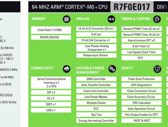
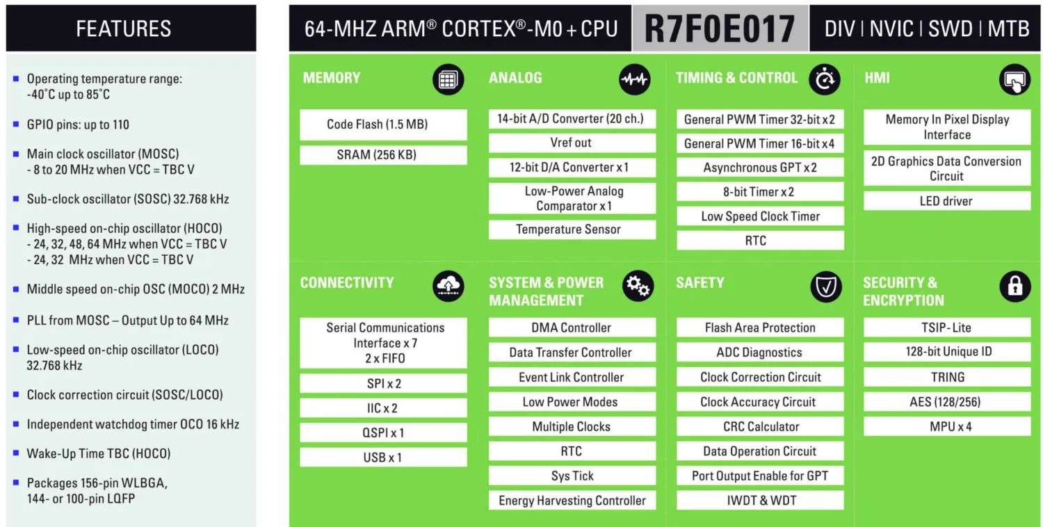
Renesas, one of the world’s very top MCU manufacturers, is heralding its new FD-SOI based R7F0E017 for energy harvesting applications. In an in-depth article in the May 2019 edition of EENews Embedded, Renesas Product Marketing Manager Graeme Clark detailed the new chip, which is sampling this year. It’s a fascinating read, with lots of explanations about how SOI enables the cutting-edge features (like an integrated energy harvesting controller) – you won’t want to miss it. BTW, here at ASN we’ve been covering the origins of this technology since 2005.They call it SOTB, for Silicon On Thin Box, but it is indeed their flavor of FD-SOI. The work started at Hitachi in cooperation with Renesas with a paper that debuted at IEDM 2004, then moved along through the series of mergers that resulted in the offering at what is Renesas Electronics today. Here are some key quotes from the article:“The new SOTB process can now offer active mode current of less than 20 µA/MHz and leakage currents down to 150 nA, while still allowing the development of devices with reasonably high clock rates, large embedded flash memories and SRAMs on chip. This combination of integration and power consumption will make devices developed on this process ideal for energy harvesting applications. The result of this new process is that we can develop a new generation of microcontroller products.” “The use of the Silicon on Thin Buried Oxide technology on this new device has resulted in some unique low power characteristics. The first device has the following features and future devices using this process could offer even lower power consumption. Active current of 20 µA /MHz Standby Current of 200 nAADC operation 3 µA @ 32 kHz256 Kbyte SRAM with 1 nA / Kbyte standby current” “The R7F0E017 is able to run safely from a pure energy harvesting power source due to the operation of the Energy Harvesting Controller. The device can operate from a wide range of potential energy sources including solar power, vibration, pressure and temperature difference, and many others. The integrated energy harvesting controller, supported by very few inexpensive external components, completely manages the cyclic wake-up sequence of the microcontroller, only using the extremely low energy harvesting source current.”Click here to read the full article on the eenewseurope website.
Read More
2019 will be a busy fall for the SOI Consortium and our members.First off are the SOI Consortium events in Shanghai and Tokyo, which are very popular indeed. We now have the dates locations locked in, so you’ll want to mark your calendars:Shanghai: 16 17 September 2019, FD-SOI Forum / RF-SOI Workshop. Both days will be held at the Pudong Shangri-La Hotel in Shanghai. The first day will focus on FD-SOI. The second day is all about 5G and RF-SOI. These are huge events – to get an idea of the magnitude, you can read our coverage of the 2018 event. Tokyo: 30 31 October 2019, Japan SOI Design Workshops. This year both days of workshops will take place in the Yokohama Landmark tower. The first day will be devoted to FD-SOI; the second day turns to More-Than-Moore – especially photonics and MEMS. Last year’s workshops were packed with excellent presentations and panel discussions, which we covered here. The SOI Consortium and members will also be giving talks at Semicon Europa, which is being held 13 – 15 November 2019 in Munich, Germany. The programs are currently being finalized. As soon as they’re ready, we’ll be sure to let you know so you can register and/or share the news with your colleagues and clients. But in the meantime, make sure you save the dates.Would you like to check out the presentations given at Consortium events in previous years? If you hover your cursor over the Events tab at the top of our home page, you’ll get a drop-down menu of events for the last five years (we’re working on adding more – we’ve been doing these events for over a decade!). Click through to any past event and you’ll land on a page where you can download most of the presentations that were given there. Of if you’re looking for past presentations given by any particular company, use the search engine at the bottom of any page on our website. S3SYou’ll also find many of our members at the IEEE/EDS S3S Conference in San Jose, CA, October 14 – 19th. S3S (formerly known as The SOI Conference) has been running in various forms for over 30 years. They always have an excellent line-up of speakers, plus it’s a great opportunity for networking with researchers from across the worldwide SOI ecosystem. BTW, while the deadline for general paper selection has already closed, papers of exceptional merit are currently being accepted for their Late News Sessions. See the 2019 Call for Papers for more information – those Late News papers need to be received by 23 August 2019 for consideration. Also, IEEE S3S Conference will once again host a full-day short course and a half day tutorial. These are very popular. The short course this year will be on SOI Design and Technology for Analog and Mixed Signal. As of this writing, the program is still being finalized, but more will be announced in the next few weeks, so check back on their website soon for updated information.Member EventsAnd finally, don’t forget to learn more about the offerings from and in support of the SOI ecosystem at our members’ events around the globe, including: GlobalFoundries – GTC | Samsung Foundry – SFF | ST – Technology Tour | Synopsys – SNUG | Cadence – CDNLive | Silvaco – SURGE | Arm – TechCon | NXP – Tech Days | Leti – Events | imec -Events |
Read More