downloadGroupGroupnoun_press release_995423_000000 copyGroupnoun_Feed_96767_000000Group 19noun_pictures_1817522_000000Member company iconResource item iconStore item iconGroup 19Group 19noun_Photo_2085192_000000 Copynoun_presentation_2096081_000000Group 19Group Copy 7noun_webinar_692730_000000Path
Skip to main content
Default Banner Image

Technology and Trends

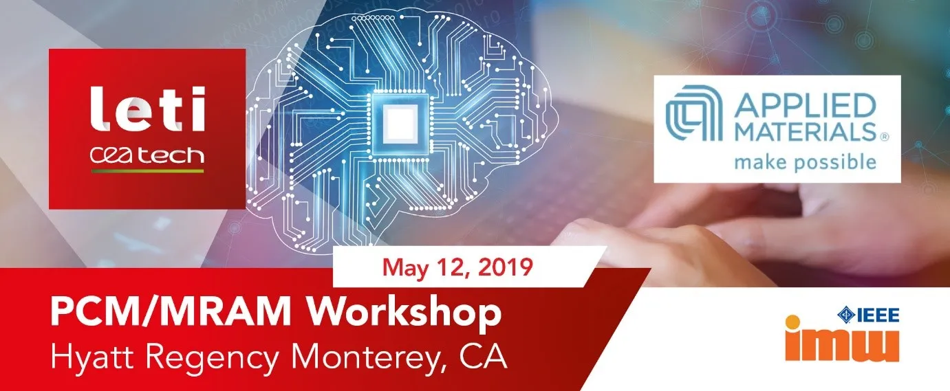
Two of the big, recent breakthroughs in memory technology – eMRAM and ePCM – have gotten their start in volume manufacturing on 28nm FD-SOI. In conjunction with the 2019 IEEE International Memory Workshop, SOI Consortium members Leti and Applied Materials have teamed up to give a technical program to explore short-term and long-term memory solutions. While the workshop is not specific to SOI, given the recent foundry announcements about ePCM and eMRAM for FD-SOI, the organizers predict it will be of particular interest to those following the greater SOI ecosystem. The event takes place at the end of the Sunday IMW tutorial day, starting at 5:30pm at the Hyatt Regency in Monterey, CA. Please see this page for the program and registration information. Here is the program: Emerging Non-Volatile Memory Promises Toward New Energy-Efficient Design and Applications - Michael Tchagaspanian, VP Business Development, CEA-Leti Technologies That Enable MRAM and PCRAM in Volume Manufacturing - Kevin Moraes, Vice President, Metal Deposition Products, Applied Materials Technology Improvements Directions of Emerging Non-Volatile Memory for New Applications Solutions - Etienne Nowak, Head of Memory Laboratory, CEA-Leti Integration Schemes and Challenges for New Memories in a New Artificial Intelligence Era -Michel Frei, Director, Advanced Product Technology Development, Applied Materials Jean-Eric Michallet, Head of Leti’s Microelectronics Components Department, Silicon Component Division is one of the organizers. Here is his overview: FD-SOI is expected to be a long-lived technology. It enables planar CMOS scaling and accommodates a great deal of More-than-Moore developments where its ability for low power and great analog performance can make a difference for IoT, Automotive, Machine Learning or 5G applications. But to do this it requires a high-performance and cost-effective non-volatile embedded memory option. The incumbent Flash cell is reaching the end of its roadmap due to the difficulty of shrinking the bitcell and manufacturing, as well as the finished wafer cost increase. Back-end integrated Random Access Memory in advanced CMOS process has been explored for many years now as a competitive solution for fast-write and low-voltage non-volatile embedded memories. Foundry availability of embedded Magnetic RAM and Phase Change RAM for FDSOI 28nm platforms has been announced recently, showing that these technologies have now reached industrial maturity. CEA-Leti and Applied Materials invite you to attend a technical program to explore short-term and long-term memory solutions, from early research to industrialization. Registration is open, free, and available to all IMW attendees, and others. However, as seating is limited and as we have already several participants pre-registered, registration is by invitation only and early registration is recommended. If you are interested, please email Jean-Eric Michallet. The event is presented in conjunction with the 2019 IEEE International Memory Workshop, to be held on Sunday, May 12th, 2019, Hyatt Regency, Monterey CA, starting at 5:30 pm.
Read More
Takeaway #1: As NXP VP Ron Martino noted in his opening keynote at the recent SOI Symposium in San Jose, FD-SOI is the technology platform for enabling edge computing, and ultra-low power is the sweet spot. Organized by the SOI Consortium with support from our members, the recent SOI Symposium in Silicon Valley was an enormous success. Close to 300 decision makers signed up – more than double what we saw just a couple years ago. Attendees spanned the ecosystem: from end-users to design to foundries and right up to the investment community. The presentations and panel discussions were absolutely terrific, and almost all are now freely available - click here to get them.The focus was heavily on FD-SOI this time, but some very interesting RF-SOI talks were given as well. This was a day packed with presentations by players from across the SOI ecosystem. In this post, we’ll only cover a few. But the others will follow quickly, so watch this page. And now without further ado, let’s dive in.NXP: In the Sweet SpotNXP VP Ron Martino presenting at the 2019 SOI Symposium in San Jose.NXP is designing FD-SOI into many new products, said Martino, GM of the i.MX Processor Application Product Line. There’s a new wave of products – generically you could call them IoT but in fact they’re found throughout the industry. It’s about interacting with the cloud, so edge processing is critical. His presentation, Embedded Processors for Future Applications, is now freely available for downloading from our website.The new i.MX7ULP is a great example of ULP in the sweet spot. From a design standpoint, it leverages IP, power optimization, and what he described as “starter biasing”. That gets them the long battery life with 2D 3D graphics they need for wearables and portables in consumer and industrial applications.NXP slide 10, SOI Symposium, San Jose '19 (Courtesy: NXP)Having deepened their expertise in biasing, NXP has now moved on to “advanced biasing” for the next generation of products. For example, the i.MX RT ULP (real-time, ultra-low-power) series are “cross-over” processors, which Martino says are the “new normal”. They deal with a high number of sensor inputs. The i.MX RT 1100 MCUs, which have been qualified for automotive and industrial applications, are breaking the gigahertz performance barrier with a low-power, 28nm FD-SOI process.Another new product leveraging advanced biasing is the i.MX RT 600. They’ve done hardware acceleration on specific functions and optimized around visionand voice integration at low cost and power.As shown at Embedded World '19, automotive app for NXP'x i.MX 8, which is on 28nm FD-SOI. (Courtesy: NXP)Likewise for the i.MX 8 and 8X subsystems for automotive and industrial applications. At Embedded World, they showed it driving advanced OLED screens, cameras (for parking, for example), V2X, audio, user monitoring (like driver pupil tracking), and integration into the windshield in a heads-up system. This is the high end of the capability of 28nm FD-SOI, he said. It’s a 6 CPU core system with multiple operating systems, about which he said: “It’s the dashboard...it’s amazing.”BTW, in another presentation, CoreAVI, which builds avionics, automotive and industrial products on NXP’s i.MX 8, addressed safety. You can get that here.FD-SOI enables a scalable solution for real-time and general compute with the lowest leakage memory, the best dynamic and static power, Martino concluded. NXP’s leadership in body biasing is enabling edge compute, and we can expect to see more content coming soon.In another NXP presentation later in the day, Stefano Pietri, Technical Director of the company’s Microcontrollers Analog Design Team caught a lot of people’s attention. A wave of cameras went up to capture each of his slides in Analog Techniques for Low Power, High Performance MPU in FD-SOI – but you can get the whole thing now from our website. It’s a very technical presentation, in which he details the many ways FD-SOI makes the analog team’s job easier, enabling them to get performance not available from bulk technologies. They developed a lot of in-house expertise and IP (see slide 16 for a catalog of the IP).Samsung: Enabling LP Endpoint ProductsTim Dry, Samsung Foundry Director of Edge Endpoint, SOI Symposium, San Jose '19Tim Dry, Director of Foundry Marketing: Edge and End Point presented Samsung’s FDS with MRAM: Enabling Today’s Innovative Low Power Endpoint Products. In a telling first, Samsung has made this presentation available on our website.FD-SOI covers the wide range of requirements for intelligent IoT, he explained: from high to low processing loads; and active to dormant processing duty cycles. That includes chips that will last for ten years, and need to be able to wake up fast and kick right into high performance. These products are 50% analog, and packaging is part of the solution (especially for the RF component).Samsung has been shipping 28nm FD-SOI (which they call 28FDS) since 2015, first in IoT/wearables, then in automotive/industrial and consumer. Yields are fully mature. In March 2019, they announced mass production of eMRAM on 28FDS. It’s a BEOL process, adding only 3 masks. It cuts chip-level power by 65% and RF power by 76% over 40nm bulk with external memory. Beyond the fact that it's 1000x faster than eFlash, eMRAM also has other advantages that make it especially good for over-the-air updates, for example.Samsung Foundry FD-SOI IP slide, SOI Symposium, San Jose '19 (Source: Samsung Foundry Keynote at SOI Symposium 2019, USA)Samsung also has RF and 5G mmWave products shipping in 28FDS. The company has a fantastic ecosystem of partners helping here, said Dry. In AI at the endpoint, they’re shipping IoT products for video surveillance cameras: some are high speed, but some are also low speed – it depends on the detection use case. And most importantly for the design ecosystem, the IP is all ready.Next up for Samsung is 18FDS, which will ship this year with RF, then in 2020 with eMRAM. 18FDS, Dry said, is optimized for power reduction. Compared to 28FDS, it’s got 55% lower power consumption, 25% less area and 17% better performance at the same power. You’ll hear more about it as well as their design services if you’re at the Samsung Foundry Forum in May (registration info here).ARM’s Biased ViewsKelvin Low, VP of Marketing for Arm’s Physical Design Group (PDG) gave a presentation entitled Biased Views on the Industry’s Broadest FDSOI Physical IP Solution. By way of background, Arm and Samsung Foundry recently announced a comprehensive, foundry-sponsored physical IP platform, including an eMRAM compiler for 18FDS. In case you missed it, at the time Arm Senior Product Marketing Manager Umang Doshi described the offering in an Arm Community / Developer physical IP blog, which Arm graciously agreed to share with ASN readers. Slide 9 from Arm's presentation, Silicon Valley SOI Symposium 2019.At the SOI Symposium, Low emphasized to the audience that Arm now has the broadest range of FD-SOI + IP solutions. It addresses mobile, consumer, IoT, automotive and AI/ML. There are 18FDS POP (processor optimized pipe) packages for Arm Cortex-A55, Cortex-R52 and Cortex-M33 processors. IP integrates biasing and a number of standard PVTs (corners). And since the Samsung platform is foundry-sponsored, it’s free.Slides 6 and 11 from Arm's presentation, Silicon Valley SOI Symposium 2019. The goal of POP IP is to enable partners to implement and tapeout Arm cores with the fastest turn-around time and best-in-class PPA while maximizing the benefits of process technology.Arm did a test chip with eMRAM, which they’ve just gotten back. It’s functional (some details are available in slide 14 of their presentation), and the company is now preparing a demo board that they’ll be showing shortly. Watch this page!That's all for this post. The next post -- part 2, covering presentations by Synaptics, GlobalFoundries, STMicroelectronics, Dolphin Integration and Anokiwave -- is now available. Click here to read on.

Read More
New MEMS-based products are constantly emerging, fueled by the Internet of Things (IoT), autonomous driving, smart manufacturing and healthcare applications. The MEMS pressure sensor market is no exception to this trend1. Its growth has been driven mainly by automotive applications such as tire pressure management system (TPMS) regulations in China, fuel and ignition systems, thermal systems, oil-pressure monitoring, and indoor and outdoor navigation systems. Easy to customize and integrate, miniature, sensitive, accurate and low-power MEMS devices are especially well-suited to the accuracy, power consumption, sensitivity and miniaturization that pressure sensors require.Yet MEMS design also presents some specialized challenges, such as a strong coupling between fabrication technology and design. Complex physical structures that exhibit non-linear behavior, custom packaging requirements, and a final product that requires integration with surrounding CMOS circuitry are just a few examples. What’s more, there is a lack of standardized processes and process validation in MEMS design ecosystems. Pressure Sensor (Courtesy: X-FAB) As with other products based on MEMS technology, designers must increasingly customize pressure sensors for higher performance – sensitivity and linearity, in this case – while decreasing their package size. Designers can accomplish the task by studying sensor performance and manufacturability using computer models prior to fabrication. This can ensure that the sensor meets its required specifications while simultaneously reducing manufacturing cycles and cost.The Power of CollaborationThis is where strong collaboration among EDA providers, MEMS technologists and designers delivers tangible benefits. EDA providers and MEMS foundries can collectively help MEMS designers to incorporate foundry process constraints into their designs.In the semiconductor industry, first-pass successful silicon relies on standardized manufacturing processes, thorough technology characterization, accurate model generation, established simulation and verification, and extensive reuse of proven design blocks. In the MEMS world, where processes and products are developed concurrently, and processes change with every product, is it possible to adopt standardized processes, design methodologies, and tools that enable efficient reuse of existing technology and design knowledge? The challenge lies in maintaining the flexibility to optimize products for a diverse array of requirements. The ideal design platform should ease sharing of technology and design data between the foundry and its customers, enabling two-way collaborative development and allowing foundry technologists to easily perform a feasibility assessment of a customer’s project. This approach offers important benefits, allowing designers to explore and evaluate the suitability of a foundry’s process technology in their unique application. It also supports accurate prediction of device performance prior to fabrication and reduces costly build-and-test cycles. Combining standardized manufacturing processes, MEMS process design kits (PDKs), and a proven design flow are the starting point for development of manufacturing-ready designs.A Real-Life Example using Pressure SensorsAn EDA company, Coventor (a Lam Research company), along with MEMS foundry partner X-FAB, collaborated to develop a PDK that would ensure that manufacturing constraints are automatically considered early in their design process. The design flow is based upon an X-FAB fabrication platform that supports multiple process options for the manufacturing of absolute and relative MEMS pressure sensors. The PDK is a “golden container” for all the process and material characteristics of the silicon membrane and substrate, glass, passivation layers, and piezoresistive components. It enforces material properties and guarantees their correct implementation during the simulation. It also includes a component library containing ready-to-use, 3D parameterized devices (such as membranes and resistors), all pre-designed with foundry-supported materials to support their respective design rules. The components are readily partitioned for optimized meshing and simulation, saving design and simulation time. Figure 1: The elements and design flow of the PDK designed by Coventor and X-FAB. (Courtesy: Coventor)Designers can use components from the library to create a custom design — which might include different membrane shapes and sizes, and resistors of varying shape, size and position — to simulate the impact of different technology variants (such as resistor doping profiles, membrane and substrate thickness, glass material properties, and passivation schemes). This allows them to anticipate the effect of these design changes on sensor sensitivity for varying pressure and temperature regimes.Extensive validation of the pressure sensor design platform is currently underway. So far, the simulations have exhibited very good correlation to actual device measurements across a range of pressure and temperature conditions, including predictions of non-linear behavior for various pressure sensor designs. At the same time, the simulation accounts for mechanical membrane properties and piezoresistivity. With this type of design platform, a foundry can provide guidelines to help customers select both the fab technology and design features that lead to an optimal design solution. Figure 2: Simulation results depicting mechanical displacement in a pressure sensor design (Courtesy: X-FAB) Let’s Face the Next Challenges…A complete design platform for MEMS must eventually include not only MEMS device design, but system integration functions, such as the application-specific integrated circuit (ASIC) design and packaging/assembly of the product. In addition to the design verification that the PDK provides, additional partnerships among foundries, integrated device manufacturers (IDMs), research centers, equipment suppliers, and EDA vendors will help to define requirements and solutions that address every level of design and production. These might include tasks such as describing standardized material properties and process specifications, creating accurate foundry-proven design models, and defining requirements for system-level simulation. In the future, PDK simulations might even include up to tape-out and physical verification. To learn more about this collaborative PDK development work, please click here for the whitepaper.Christine Dufour, MEMS PDK Program Manager, CoventorChristine Dufour is the MEMS PDK program manager at Coventor. She has more than 20 years of experience in the semiconductor industry, leading process design kit development for BiCMOS and CMOS processes at several major semiconductor companies. Ms. Dufour has also worked as a product manager in the RF design environment area. In addition to her extensive experience in MEMS PDK development, she is an expert in all aspects of MEMS design flow and design tool development. Ms. Dufour received an engineering degree at Technological University of Compiegne.For more information on Coventor, a Lam Research Company, visit: https://www.coventor.com/ Viraja Sharma, Development Engineer, MEMS Simulation Design, X-FABViraja Sharma is a development engineer for MEMS Simulation Design at X-FAB. Her work involves the design and simulation of MEMS inertial and pressure sensors. Prior to her tenure at X-FAB, Ms. Sharma performed similar duties for other semiconductor companies. She received her Master of Science degree in Micro and Nano Systems from TU Chemnitz, where she studied MEMS and micro technologies.For more information on X-FAB, visit: https://www.xfab.comCoventor and X-FAB are members of SEMI-MEMS Sensors Industry Group that connects the MEMS and sensors supply network, enabling members to address common industry challenges and explore new markets. 1 Market research firm Yole Développement predicts that MEMS pressure sensors alone will become a $2 billion market by 2023. See: https://yole-i-micronews-com.osu.eu-west 2.outscale.com/uploads/2019/01/YD18018_MEMS_Pressure_Sensor_Market_Yole_Developpement_2018_Sample.pdf
Read More
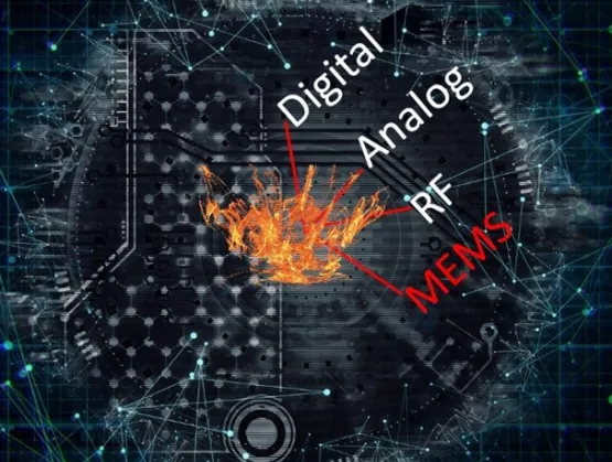
Creating a custom Internet of Things (IoT) IC is challenging because it involves multiple design domains (digital, analog and RF). Creating a sensor-based IC that combines electronics that use the traditional CMOS IC design flow with a MEMS sensor on the same silicon die, however, can seem impossible. Couple the co-design and verification challenges with a lack of traditional process design kit (PDK) support for MEMS, and you have a tough road to travel to get your IoT designs to market.What can we do to make the sensor-based IoT design community successful?Understanding the ChallengesThe sensor-based IoT IC typically features a MEMS sensor (and optional actuator) that interact with the real world. Analog and digital circuitry processes the signals and sends them to a CPU. The CPU provides the “smarts” to process the data from the sensor and then sends processed data via a radio to the Internet; alternatively, the CPU could activate the actuator. A typical sensor-based IoT IC (Source: Mentor: A Siemens Business) Based on the complexity of the system, designers face many co-design challenges: Analog design requirements imposed by MEMS: MEMS devices often require high voltages and multiple power supplies; they emit small signals that need amplification and conditioning; and they are sensitive to the environment and require calibration. Design flow interactions: Parasitics from MEMS devices might affect circuits and vice versa. Circuit designers need MEMS models for impedance and timing. Integration: MEMS devices operate at different timescales than circuits, which adds a layer of complexity. Compounding the problem is a lack of MEMS PDKs and methods to tie together ICs and MEMS PDKs for integration and cross-verification. After conquering the co-design challenges, the design team has to address mixed-domain simulation challenges that include: Simulating the system: This requires verification of MEMS, digital, analog and RF circuitry with embedded software that runs on the CPU. Timescales: These vary widely, from a single deflection of the MEMS transducer in femtoseconds to a seconds-long simulation of the embedded software performing a measurement and transmitting data. Simulation time: Simulation of a behavioral digital design is extremely fast. However, the system simulation requires stand-in models that incorporate the behavior of the analog and MEMS block to simulate in an acceptable amount of time. The challenge of timescales for co-simulation. (Source: Mentor: A Siemens Business) MEMS is the KeyThe reality is that it’s the MEMS device that adds extra complexity to the sensor-based IC design and verification flow. To amplify the problem, the MEMS manufacturing process is not nearly as mature as the standardized IC process. For example, the standardized IC process includes ready-made PDKs that include everything designers need to move through design and verification flows. Foundries often provide soft and hard IP to quickly build-out design, and EDA tools provide high levels of automation enabled by abstraction and a standardized IC flow. How will MEMS-based design evolve?MEMS-based design must catch up to the standardized IC process. The first step is providing MEMS PDKs that include: Multi-physics domain design rules and material properties Packaging information Wafer and bonding information Fabrication information We must also tackle issues associated with these PDKs, including: Ownership, distribution and maintenance of the PDKs Consensus on the contents of the PDKs Merging of CMOS and MEMS PDKs The industry needs to move toward standardized MEMS manufacturing processes with available PDKs. Companies must provide IP and recommend structured design methods for co-design and verification of ICs that incorporate MEMS. How can EDA help with these flows?The EDA ContributionEDA companies must work with teams in the MEMS IC co-design space, collaborating with MEMS fabricators to help enable PDKs. By incorporating PDK support within their own tools, EDA companies can provide an integrated custom IC flow that allows teams to design and verify MEMS-based ICs. For details about this flow, click here to download the Mentor whitepaper: Fusing CMOS IC and MEMS Design for IoT Edge Devices.Greg Lebsack brings 25 years of executive and technical management experience — along with a proven track record of building strong teams and delivering predictable results — to his role as general manager of the ICDS division of Mentor, a Siemens Business. Lebsack joined Mentor in 2015 after that company acquired Tanner EDA, where he was president. Prior to Tanner EDA, he held management and technical positions in a number of different industries and companies, including Sprint, General Electric and McKinsey Co. Greg holds a bachelor’s degree in business administration from Northern Arizona University.Greg Lebsack recently presented on the topic of Integrated Co-design of MEMS/IC at the MEMS Sensors Technical congress, a technical conference organized by the MEMS Sensors Industry Group.
Read More
Smart car technology is on the fast track. According to a forecast by the Consumer Technology Association, revenue for North American technology will reach $398 billion in 2019, with sales of emerging technologies related to automotive electronics alone expected to hit $17 billion, a 9 percent increase over 2018. Growth of automotive electronics in the semiconductor application market is on pace to exceed 10 percent for the first time, with a 11.9 percent annual compound growth rate from 2017 to 2022, said Peng Maorong, research manager of ITRI Industrial International. Today, automotive electronics trails only personal computers and mobile devices in driving semiconductor market revenue. For its part, Automotive World 2019, the world's largest exhibition for advanced automotive technologies, has drawn even more attention in recent years. The event consists of six exhibitions, including automotive electronics technology, auto parts, drive systems, lightweight materials, autopilot technology and car networking, and featured demonstrations of compelling technologies including an AI deep learning module (Xilinx) and high-speed car intranet technology (Israeli manufacturer Valens). Toyota is also on the cutting edge of automotive electronics with the rapid maturity of its semiconductors, AI technology and materials, and complete network technology. The carmaker is no longer just a pure-play automotive manufacturer. Instead, the automotive giant is positioning itself as a car service provider (mobility service provider) and plans to team with ride-sharing providers such as UBER and Didi and other automotive technology providers in the future.Taiwan, with its strong semiconductor industry chain and a complete ecosystem of information communication, will be a key force in the automotive market as the region looks to cross-industry and cross-border cooperation to help power the market. To help the automotive electronics industry seize the market promise of smart cars, SEMI established the Global Automotive Electronics Advisory Committee (GAAC), with members including Audi, Bosch, Denso, Ford, Honda, Nissan, Volkswagen, Amkor, Infineon, NXP, Synopsys and Wanghong. More than 30 international companies, spanning Europe, the United States, Japan and other regions are represented on the committee. The committee met for the first time this month in Taiwan to help leverage the prowess of Taiwan's microelectronics supply chain in advancing international automotive electronics, better link Taiwan to international trends, and give Taiwan a bigger voice in the emerging smart car market, and create more opportunities for resource integration across borders. To learn more about GAAC, contact Helen Chen Chen Huiyu | Email: [email protected] | Phone: (03) 560-1777 #112.Extended reading: smart car Baihua Qi will be the next wave of killer applications (on)Emmy Yi is a marketing specialist at SEMI Taiwan.
Read More
Have you ever wondered if you could “feel” what it’s like to revisit your favorite vacation spot while sitting on a couch in your living room? How about walk through a restaurant overlooking the water’s edge as you enjoy a savory dish, while still sitting on that couch?If you follow trends in consumer electronics, you probably imagined a virtual reality (VR) headset that uses a visual interface to simulate the ambiance of the restaurant as you use a voice interface to scroll through the restaurant’s menu. While the tech world has made great progress in evolving the visual and voice interfaces of VR, immersive virtual food-tasting also requires a digital interface that supports a sense of smell and taste. In fact, the National University of Singapore is conducting research on the topic (see the video), and Project Nourished claims to enable “eating and drinking in a whole new way – by hacking vision, gustation, olfaction, audition and touch – with or without caloric intake” – through VR.We’ve already come a long way in our quest to replicate human senses such as touch, vision (via biometric authentication) and voice to build user interfaces to interact with the digital devices around us. In fact, every invention that permanently changed the consumer electronics landscape in the last few decades has in turn brought to life one of these user interfaces (UI). For example, smartphones proliferated touch, video games such as Nintendo Wii and Sony Xbox brought gesture, and most recently, smart speakers and VR headsets have increased the adaptation of voice and vision.Complexities of UI DesignUI design is a complicated task that builds upon years of research in neuroscience, cognitive thinking and engineering. It must also account for individuality because users interact differently with their digital devices. Some, like me, use their left hand predominantly when interacting with a gaming console. Some have a heavy accent, which can make speech recognition difficult, while those with a hearing disability may prefer touch over voice as a user interface. Application, context and proximity of the device to the user also affect UI. For example, a user interacting with a smartphone at home has the option to touch or speak to the device whereas voice is the safest means to communicate with a car’s infotainment system while driving.Consumers often bring their digital devices wherever they go, but still expect a consistent user experience. Therefore, a natural user experience is the key to UI adoption. A multi-sensory approach combining voice, vision and/or touch could prove the most practical solution. For example, if I were to access my account at a bank ATM, I would prefer visual- or touch-interface authentication for security reasons, but I would still want to use a hands-free voice interaction to switch between the different menus on the machine. In this case, a combination of UIs could provide a more natural multi-sensory experience, albeit one that needs a careful design.UI technology development and adoption are largely influenced by the top four players in the consumer electronics industry – Apple, Amazon, Google and Samsung. Apple pioneered the touch interface with the invention of keyboard-less smartphones, and the rest of the industry followed suit. The introduction of Google Glass kickstarted the VR/augmented reality (AR) segment and opened new applications in the gaming and multimedia entertainment segments. While VR headsets work for gaming – and more recently for selling products and experiences – they are large and cumbersome devices that are uncomfortable to wear for extended periods. These are major hurdles for designers to solve. Voice, on the other hand, offers a hands-free user interface that is a more natural and frictionless compared to alternative UIs.A voice UI needs nothing but a voice command to interact with digital devices. However, it comes with its own complexity of varying user speech characteristics such as accent or volume. More importantly, the need to suppress various background noises for efficient use of voice UIs is critical. While edge computing and/or cloud-based artificial intelligence (AI) are critical technologies to enable battery life and performance of smart home devices, the overarching goal of conversational AI is still far from reality.From a business standpoint, the winner of the race for voice UIs must improve AI capabilities while supporting a strong ecosystem of partners. Amazon, for example, is king of this strategy. The e-commerce giant is building an Alexa Voice Service (AVS) ecosystem by way of its Alexa Fund companies and third-party integrations (partners) to realize its goal of proliferating voice everywhere. These partnerships enable the ecosystem to build end-to-end speech systems that can literally take voice interface products everywhere and promote, among other things, hardware startups that are disrupting the MEMS market with products such as environmentally robust piezoelectric microphones.Energy harvesting near-zero-power always-listening microphones, used in partnership with the AVS ecosystem, are enabling voice UI products to expand into battery-operated applications such as hands-free TV remotes, smart garbage cans, Bluetooth speakers, headsets, hardware appliances and automobiles. A good example of a unique voice UI launched at CES 2019: Housewares designer simplehuman’s voice-activated smart garbage can uses Vesper microphones and AVS. Watch the video.While the future might bring additional digital interfaces, along with multisensory experiences using vision, gesture and touch, voice UI is at the forefront of current technological innovation. Soon, Alexa might help cook dinner without intervention, even turning off the stove when food is burning through the use of a scent-detection sensor integrated with a microphone array. Voice UI continues to astound us with its possibilities, and we’re excited for the journey ahead.With more than 12 years of experience working in speech and voice applications for wireless devices, Udaynag Pisipati is a senior field applications engineer at Vesper. He holds a master’s degree in electrical engineering from University of Missouri and an MBA from Santa Clara University. A firm believer in speech as a natural user interface for human-machine interaction, Pisipati’s areas of interest include everything related to speech processing, including microphones/speakers, signal processing and machine learning.Vesper is a member of MEMS Sensors Industry Group (MSIG), SEMI technology community.
Read More
Editor's note: Arm and Samsung Foundry are extending their collaboration on FD-SOI, which they'll be highlighting at the SOI Consortium's Silicon Valley Symposium April 9th. In the meantime, Arm Senior Product Marketing Manager Umang Doshi described the range of projects in a recent Arm Community / Developer physical IP blog. We thank Arm for sharing this blog with ASN readers.~ ~~ Samsung Foundry and Arm FDSOI collaboration announced By Umang Doshi The challenge with designing at newer and more advanced process nodes is that things generally don’t get less complex and expensive, much as we might want this. Still, the upside to each new process node, generally, is that you can build more highly efficient and targeted devices to address more markets and applications in a timely fashion. For the complexity and cost challenges, however, there’s good news: Arm and Samsung Foundry just announced a comprehensive, foundry-sponsored physical IP platform, including an eMRAM compiler at 18FDS (18nm FDSOI). In addition, the Arm offerings for 18FDS include three POP IP packages for Arm Cortex-A55, Cortex-R52 and Cortex-M33 processor IP. The platform will help drive new leading-edge designs in power-sensitive applications in 5G, artificial intelligence (AI), automotive, Internet of Things (IoT), and other market segments. It’s the industry’s first, fully comprehensive physical IP platform that includes an eMRAM compiler at 18FDS. 28nm: Before the breakthrough One of the most widely embraced nodes, 28nm the so-called “forever node,” has done wonders for industry innovation over the years. However, leakage power is still challenging for planar transistors. Engineers deployed high-K metal gate (HKMG) at 28nm, to combat leakage, but it’s still an issue. That’s because the channel underneath the gate is too deep and too far from the gate to be well-controlled, which results in higher leakage power. Solutions for the leakage issue have prompted designers to embrace FinFETs and FDSOI (fully-depleted silicon-on-insulator) with thinner channels that enable greater control by the gate. Indeed, FDSOI is gaining traction in the market place. By construction, 28nm FDSOI enables much better transistor electrostatic characteristics versus conventional bulk technology. 28nm FDSOI offers: Wide Forward/Reverse Body-bias range and flexible Poly bias (PB) range to tradeoff power/performance. Better performance and power than bulk process technology. Better resistance to radiation and SER. Less sensitive to variability because there’s no channel doping. Ultra-low power voltage (operating at low voltages in the hundreds of millivolts range). Easy migration from bulk versus the previous SOI version, PDSOI (partially-depleted silicon-on-insulator), required unique timing and power models. What’s more, there are cost benefits today and more forecast for the future. Arm and Samsung Foundry extend FDSOI leadership from 28FDS to 18FDS In 2018, Arm announced the industry’s first Embedded MRAM (eMRAM) compiler IP built on Samsung Foundry’s 28FDS process technology. Since the announcement, Arm has engaged with several Samsung Advanced Foundry Ecosystem (SAFETM) partners on a landscape-changing collaboration to deliver the industry’s first 28FDS eMRAM-enabled IoT silicon system demonstrator telling the Arm IoT story on Samsung Foundry silicon. Coupled with Arm’s IoT ecosystem, Pelion IoT Platform and Platform Security Architecture (PSA) solutions, this 28FDS eMRAM-enabled IoT demonstrator will showcase a new-generation of secure and energy-efficient IoT edge devices which integrates software stacks offering secure boot, firmware updates, on-chip storage, chip to cloud communication and device/software provisioning. The combination of 28FDS and eMRAM non-volatile memory brings new opportunities for a new class of highly integrated and energy-efficient designs. We’re thrilled that Samsung Foundry has extended its successful collaboration on FDSOI technology from 28FDS process to 18FDS. With the new platform, 18FDS is a cost reduction solution with lower power and same back end of line (BEOL) as 14nm FinFET. It has RF and eMRAM support to enable the widest range of different applications. “18FDS is the next-generation node on Samsung's FD-SOI roadmap with enhanced power, performance, and area (PPA)," said Jaehong Park, executive vice president of Design Platform Development at Samsung Electronics. “The relationship between Samsung Foundry and Arm stretches back more than a decade and has helped put the right design technology in the hands of the world’s leading designers. The enhanced PPA from our 18FDS process combined with Arm cores and Artisan Physical IP will again bring the cost and time-to-market advantages to enable the competitive and differentiated SoC designs.” Highlights on Arm-Samsung 18FDS platform Includes seven memory compilers, three logic libraries, two (1.8 and 3.3V) GPIO libraries, three POP IPs and the eMRAM memory compiler. Supports automotive AEC-Q100 Grade 1 design requirements, and comes with ASIL-D support and a complete automotive safety package. Utilizes back biasing supported by the FDSOI technology to help achieve low leakage by using reverse body-bias technique or a performance boost using forward body-biasing. This is a key differentiation of 18FDS platform. Supports Logic Corner Generator (LCG) and Memory Compiler Corner Generator (MCCG). LCG and MCCG products allow designers to generate custom corners with body-bias voltages to take the maximum advantage of body biasing power-performance flexibility. 18FDS will help enable the development of new devices connecting consumers in entirely new ways, whether it’s in AI, 5G mobile, automotive or other areas. The platform will be available in late 2019. Arm's Physical Design Group has a track record of successful implementations with Samsung Foundry across multiple generations of process nodes and products. Besides 28/18FDS, Samsung Foundry and Arm also have 14LPP/LPC, 11LPP, 7LPP and 5LPE platform collaborations. Interested in knowing more about Artisan Physical IP at 28/18FDS? Come join us at SOI Silicon Valley Symposium on April 9 at Double Tree by Hilton, San Jose, California. During the event, you will have the opportunity to hear how Arm and other industry leaders work together to accelerate the adoption of FDSOI technologies including products and applications. Alternatively, you can also reach out to us with your inquiry.
Read More
Semiconductor, electronics and equipment manufacturers today face a number of logistics and supply chain challenges that could be overcome by systems providing a secure, tamper-resistant, single source of truth. Chief among these challenges is limited data sharing due to data security barriers among suppliers, shippers, manufacturers and test houses, an impediment to achieving optimal product quality and regulatory compliance. Additionally, inefficient and inadequate processes for tracking goods make it more difficult to isolate shipping problems, track faulty parts and verify product authenticity. Counterfeiting has become a serious problem that costs US-based semiconductor manufacturers $7.5 billion annually.How Blockchain Can Help Clear Data Sharing BottlenecksBlockchain functions could help alleviate many data sharing pain points in manufacturing. Blockchain’s distributed functionality, bundled security measures, and associated features such as smart contracts have the potential to help manufacturers quickly trace goods, manage records transparently, and automate supply chain processes and payments. No isolated blockchain platform would solve all of these problems on its own. But, when combined with other solutions and applied to particular use cases, blockchain has the potential to optimize operations and foster an environment of trust and collaboration among consortium members. Three core features of blockchain make it a valuable technology for manufacturing: Distributed and immutable system of record. With a distributed system of record in the blockchain network, there is no "central" data store controlled by one organization. The distributed ledger provides all participants with a view into the data, thus increasing transparency, data distribution timeliness, information sharing, and data access. Security also improves as there is no single central data store open to external attacks. Once data is inserted onto the chain, it cannot be easily changed. Security and Trust. Blockchain integrates best-of-breed cryptographic mechanisms to guarantee the digital identity of the network participants and secure the privacy of the data stored to enable role-based data access. It brings trust to a potentially trustless environment without the need for a centralized third party. Smart Contracts. Smart contracts are embedded business logic that can be added to a blockchain. They enable the automation of many processes and the secure handling of contracts. Blockchain Use Cases in ManufacturingIn each stage of manufacturing, blockchain could be applied in a variety of use cases to expedite processes and alleviate security issues. A few examples that merely scratch the surface of what may be possible follow.In pre-production, manufacturers may implement blockchain solutions for Collaborative Planning, Forecasting and Replenishment (CPFR). These systems monitor inventory levels, enabling suppliers to replenish supplies before they run low. The expensive, proprietary B2B networks used today could be replaced with blockchain as the common sharing protocol, using non-proprietary or public networks.Suppliers may also combine blockchain with IoT sensors on shipping containers to provide a tamper-resistant record of shipping conditions. This could be used to ensure that temperature and humidity tolerances for chemicals and equipment are not exceeded during transit from the supplier. The identity and materials in components and subcomponents of manufacturing equipment could be collected on a blockchain to verify compliance with environmental and health regulations. During production, a manufacturing process machine can be registered on a blockchain with a unique identity; its performance and maintenance history can be recorded. A maintenance service provider could then be automatically notified, via a smart contract, when a predictive maintenance alert is written, allowing repair of machines before they fail. In the distribution stage, customers could search the ledger for a product’s complete history, reducing counterfeiting and solidifying the origin of properly sourced goods. When faulty product is identified, the manufacturer may search the ledger to quickly locate the faulty supplier or bad test results and alert all receivers of the defective product.ConclusionWith blockchain, manufacturing can become a more collaborative process among suppliers, manufacturers and customers. Blockchain can help streamline the supply chain and inventory replenishment, improve tracking and regulatory compliance, and reduce counterfeiting. Augmenting blockchain with IoT enables use cases like predictive maintenance and monitoring of goods during transit. Blockchain is not yet mature and its business value still needs to be proven. However, it is poised to help manufacturers decrease costs and fraud, and provide customers with faster, more secure delivery, increased visibility, and consistency.More Resources on Blockchain and ManufacturingTibco is an active member of SEMI’s Smart Manufacturing Technology Community, which holds regular meetings on this and other topics. Join now to help shape the future of Smart Manufacturing. For more information on blockchain use cases in manufacturing, please see these resources. Read this Whitepaper: Blockchain and Manufacturing: A Match Made in the Factory Watch this Webinar: Blockchain and Manufacturing - A Match Made in the Factory Visit the TIBCO Blockchain Solutions page Mike Alperin is a TIBCO principal manufacturing industry consultant embedded in the Data Science team where he applies analytics, machine learning and big data technology to current industry problems. Prior to this he was the product manager for a leading commercial yield management application. He has worked at start-ups and global semiconductor manufacturing companies as a yield manager, device engineer, process engineer and failure analyst. Mike is based in Austin, Texas.
Read More
FD-SOI for RF and mmWave communications is a hot topic. In high-data rate communications like RF and millimeter-wave devices in particular, FD-SOI delivers high-performance with numerous unique advantages, making it most likely the fastest RF-CMOS technology on the market. If you’d like to take a deep dive and learn more about it, Soitec and Incize are sponsoring a free, full-day workshop in Grenoble on April 4th, 2019. Click here for registration information. The workshop follows the day after the IEEE/EDS EuroSOI-ULIS conference there (you can read about the full conference in a previous ASN post). This technical workshop will cover the FD-SOI technology platform with a focus on its compatibility with RF mmWave communications. Attendees will hear from notable FD-SOI leaders and experts from leading industry and research institutions presenting updates on key developments and building blocks across the semiconductor value chain. Topics will include circuit design, device fundamentals, simulation and characterization of RF devices, test, CMOS technology and substrate technologies enabling FD-SOI. In addition, the workshop will include an overview about how FD-SOI technology is benefiting current and future end user applications. Here’s the agenda: [caption id="attachment_15990" align="alignleft" width="945"] FD-SOI technology platform: new standards for emerging consumer electronics [Click to enlarge.][/caption]
Read More