downloadGroupGroupnoun_press release_995423_000000 copyGroupnoun_Feed_96767_000000Group 19noun_pictures_1817522_000000Member company iconResource item iconStore item iconGroup 19Group 19noun_Photo_2085192_000000 Copynoun_presentation_2096081_000000Group 19Group Copy 7noun_webinar_692730_000000Path
Skip to main content
Default Banner Image

Technology and Trends

The Single Device Traceability Task Force emerged from SEMI CAST’s identification of the need for device traceability through the supply chain — not just traceability for devices but for component parts such as semiconductor die, lead frames, epoxy, bond wires, and printed circuit boards. Eventually the work led to a draft document and preparation for SEMI’s standardization process.The Single Device Traceability Task Force’s charter is “To develop standards enabling traceable device-level identification (ID) throughout the IC manufacturing, test, and assembly processes to the point of use in the final system.” The scope of this work is to develop standard(s) focusing on key concepts, behaviors, and requirements as well as standards for enabling device ID and traceability, with considerations for various types of implementations. In addition, the Single Device Traceability Task Force is looking at anti-counterfeiting, which is closely associated with traceability.The motivation for this particular traceability standard comes from systems companies that purchase and use semiconductors in boards and systems. These companies need the ability to track devices through the supply chain for various reasons. They do not want an ad hoc situation where each system vendor develops its own requirements and specifications for device traceability. They want a standard to reduce traceability’s cost and complexity.In effect, customers want a standard that can be cited in a purchase order to their suppliers. This will require the supplier to mark (ECID, 2D code, RFID, etc.) their products with an ID unique for that supplier. The customer will verify the ability to read the ID and will reject devices that cannot be read, or disagree with the shipping information. This arrangement should propagate throughout the supply chain. As a result, the traceability draft standard developed by the Single Device Traceability Task Force looks at traceability from a system integrator’s perspective.Figure 1 captures the business problem for device traceability. Figure 1: Single Device Identification and Traceability Needs Permeate the Semiconductor Industry.Each time that a company ships product to the next company in the supply chain, it’s desirable to have traceability for the products being shipped while preserving the security of the information associated with those products. Initially, the only information that should be transferred is the device identification. In other words, the device traceability ID should not identify what the device is, nor should it provide any additional information relating to the device or its manufacture. In addition, the Traceability ID should not specify the number of devices shipped, the lot number associated with the devices, or any other information that might be of value to hackers or competitors. There is quite justifiable paranoia about the security of this information based on lessons learned.However, the whole point of traceability is to be able to backtrack a device through the supply chain when there’s a problem. Ultimately, any QA effort will need to know where the device was manufactured, when it was manufactured, the conditions under which it was manufactured, and other details that might help to discover the root cause of any problems.To get the additional information needed to troubleshoot a quality or manufacturing problem, a business relationship and NDAs (shown in Figure 1) must be in place between the various member companies in the supply chain. Traceability IDs based on the Single Device Identification and Traceability Standard will not carry that sort of information. They will simply allow analytic data to be obtained through appropriate business relationships.Figure 2 illustrates the types of fact finding that a Single Device Identification and Traceability standard would enable. Figure 2: Types of fact finding enabled by a Single Device Identification and Traceability standard. In this example, a Fabless or System manufacturer (shown in the center of the figure) might make an assembly that incorporates an MCM (multi-chip module) obtained from an OSAT (outsourced assembly and test) vendor. The MCM would bear a traceability ID on or inside the package. If a failure occurs in the MCM, the Fabless vendor contacts the OSAT, using an existing business relationship and NDA, and requests a comprehensive manufacturing report for the specific device using the traceability ID to identify the device in question. The OSAT then supplies a report to the Fabless company that provides the requested manufacturing data and any additional traceability IDs for the component parts in the MCM.The component traceability IDs in the OSAT’s report provide the Fabless vendor with the ability to track the MCM’s component die and package back to the semiconductor foundries and packaging vendor where these components were manufactured. These traceability IDs allow the Fabless vendor to request manufacturing reports for the components in question from the supplying foundries and the package vendor. Note that the reason that the reports go directly from the semiconductor foundries to the Fabless vendor as shown in Figure 2 is that the OSAT may not have comprehensive information about the function of these die and the Fabless vendor may want to keep that information private.The proposed new standard is called the “Specification for Single Device Traceability for the Supply Chain” and is SEMI Draft Document #6450. It addresses the first part of the systems integrators’ desire of being able to hold their suppliers accountable for having an established traceability scheme that would permit data analysis should the need arises. As of the end of November, the ballot proposal passed Technical Committee review and will undergo a procedural review process as part of the SEMI Standards development requirements. Once, these approval requirements are met, the specification will be prepared for publication and ready for industry adoption. Meanwhile, SEMI’s CAST Working Group and Standards Task Force will continue standardization efforts for device security and anti-counterfeiting. To join SEMI Standards activity, visit SEMI Standards or go directly to the Standards Membership Application.Dave Huntley is in business development at PDF Solutions.
Read More
Gas plasmas have become a fundamental building block in many semiconductor manufacturing processes. Plasma torches used to create these gas plasmas have three components: an induction coil, a plasma confinement tube, and a gas distributor or torch head that introduces multiple gases into the torch. RF generators supply the high-frequency electrical energy needed to transform the plasma-forming gases flowing through the torch, typically oxygen or a fluorine-bearing gas, into a plasma. The RF generators used for semiconductor manufacturing typically operate in the low megahertz or tens of megahertz frequency range and are expected to output high RF power at those frequencies for long periods. For example, ALD and CVD processes use RF generators with output powers on the order of a few kilowatts.About three years ago, a major semiconductor device maker experienced a recurring problem with its RF generators. The company found that more than half of the RF generators it deployed in its manufacturing lines were failing within the first two years of service. Further, the same model RF generators obtained from the same RF generator vendor simply were not behaving similarly when used for exactly the same processes under exactly the same conditions. Nor were these supposedly identical generators operating for consistent lengths of time before failing. Clearly there was variation from one generator to the next, even within the same model.A further complication occurred during procurement of these RF generators. Procurement people were acquiring generators using general specification requirements and these requirements were, at times, opaque to the intended process application. In some cases, equipment was being purchased in bulk quantities and then assigned to different processes on the semiconductor manufacturing lines. When these generators were deployed, they had not been designed or optimized for the specific task to which they were assigned, exacerbating the reliability problem.The RF generator suppliers felt that they would be able to supply more reliable generators if they could collaborate with their customers so that they could purpose-build their generators for the intended uses. However, the semiconductor makers preferred to keep the specifics of the manufacturing process applications for these generators proprietary, for obvious reasons. To make matters worse, customers did not always return failed units to RF generator vendors for analysis. Instead, the RF generators were sometimes sent out to be refurbished by third parties or repair depots, and then redeployed. As a result, failure analysis proved challenging to obtain.This is exactly the type of situation that SEMI’s Semiconductor Component, Instrument and Subsystem (SCIS) technical community exists to address. SCIS develops test methods aimed at measuring component defects for the greater semiconductor manufacturing community. SCIS tackled this RF generator problem and developed a standard test method for measuring specific RF generator characteristics. Using this test method, RF generator manufacturers can publish results for their generators in a standardized way that allows their customers to make fair, application-specific comparisons among models and vendors.Many aspects of an RF generator needed to be considered. A key aspect that interested integrated device makers (IDMs) and capital equipment OEMs was a transient-response test for RF generators.A transient-response test standard established by the SEMI-E135 standard did exist, but its tests were run only with 50-ohm RF output loads. SCIS decided to expand this transient-response test by adding high- and low-impedance load tests to the existing 50-ohm load test.The initial response to this plan was not enthusiastic. The semiconductor makers feared that this simple expansion of an existing test standard would not produce a test regimen that would help solve what they considered to be the real problem: RF generator reliability. However, a major semiconductor equipment OEM differed, and felt that the two additional load conditions would provide a much better understanding of an RF generator’s capabilities. A second major semiconductor equipment OEM also got involved by providing additional, valuable feedback on the developing RF generator testing standard.In the end, the general feeling in the community is that this newly revised standard levels the playing field and makes it easier for customers to compare RF generators from different generator vendors. Now that this revised SEMI-E135 standard with the additional output load resistances has been published, the SCIS technical community has gained broader support and is now digging into the creation of a reliability test standard for RF generators to meet the greater semiconductor manufacturing community’s strong need for such a standard.How SEMI Standards are MadeThis sequence of events illustrates how standards are developed at SEMI. The SCIS technical community (or some other technical community within SEMI) develops and incubates test methods until a document is ready for standardization. At that point, a SEMI Standards task force is created. Companies within SCIS work with the task force (or become the task force) to ready the document for standardization. For the SEMI-E135 revision, the list of participating companies encompassed the entire semiconductor manufacturing community including RF generator suppliers, semiconductor capital equipment OEMs, and IDMs. All stakeholders participate.Figure 1 illustrates the sequence of events that occurred during the revision of the SEMI-E135 standard, after the test methods had been developed by SCIS as discussed above. Figure 1: Timeline for SEMI-E135 RF generator test standard revision after SCIS had developed the new load tests. Balloting, as illustrated in Figure 1, is the main way that SEMI obtains global consensus in the standards-making process. To achieve this, SEMI sends out the standard ballot proposal, or in this case a major revision of an existing standard. The changes to SEMI-E135 were sufficiently extensive that it was treated as a complete rewrite to this standard.On first ballot, the revised SEMI-E135 standard received several rejection votes, which also included suggested modifications that would remove the objections. These ballot rejections caused the proposed standard to be further revised, with both technical as well as editorial changes, triggering a SEMI Standards process called a Ratification Ballot. This approach takes less time than starting the balloting process over again. The final revised standard was published in September 2018.Having all stakeholders participate in the early development of the revised standard helped move the standard through the balloting process immensely, but customer participation was especially important. In the end, the semiconductor device makers and equipment OEMs are the ultimate beneficiaries of a standard like SEMI-E135. When end customers help to drive a standard’s development, there’s added pressure to move the standard along in the standardization process and the standard is far more likely to be useful for their purposes.And that’s a very good thing.For those looking to learn more about SCIS or engage in ongoing efforts, please contact Paul Trio, senior manager of Strategic Initiatives at SEMI, at [email protected].
Read More
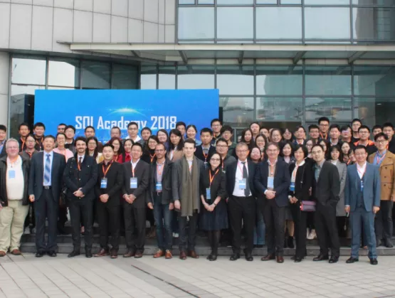
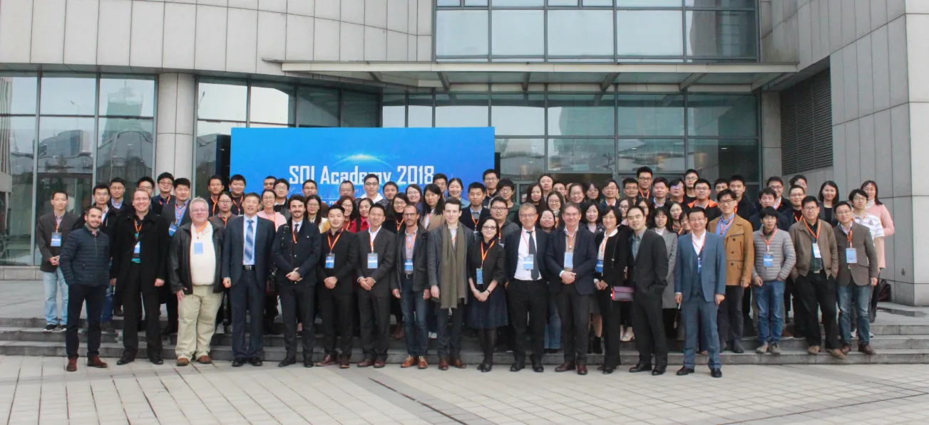
There were over 220 participants at the recent SOI Academy FD-SOI Training event organized in Shanghai. The event extended over two days, with the first day covering a basic introduction to the technology as well as the ecosystem worldwide and in China. The second day was hands-on professional training. Attendees got a comprehensive understanding of how to leverage the benefits and flexibility of FD-SOI design techniques for low-power chips including logic, mixed-signal/RF and analog blocks. They had a great line-up of experts from whom to learn – check out the agenda here. There was also a follow-up press release (in Chinese) from SITRI here. There will be more of these SOI Academy events in cities across China in the year to come – we'll keep you posted (and of course, keep checking back for news on the Consortium's Events page). [caption id="attachment_12981" align="aligncenter" width="1000"] SOI Academy '18 keynotes by: Dr. Mark Ding, CEO, SITRI; Dr. Carlos Mazure, EVP Soitec and Chairman/Executive Director SOI Consortium. Dr. Julien Arcamone, EVP Leti. (Images courtesy: SITRI). Lower right: the hands-on FD-SOI training.[/caption] The two-day seminar and hands-on FD-SOI design training was (superbly!) co-organized by SITRI and Leti, with the support of the SOI Industry Consortium at the Jiading SIMIT campus outside of Shanghai. Just to put this in perspective, SIMIT and SITRI are absolutely key players in China's chip ecosystem. SIMIT is the Shanghai Institute of Microsystem and Information Technology, one of the most venerable institutes in the Chinese Academy of Science (CAS) and one of the world's earliest pioneers in SOI. SITRI is the Shanghai Industrial μTechnology Research Institute, an international innovation center focused on globally accelerating innovation and commercialization of More-than-Moore for IoT. Both institutions are under the aegis of Dr. Xi Wang, Chairman of SITRI, Director General of SIMIT, Academician of CAS, and champion of all things SOI in China. At this Shanghai event, the participants came from industry (including big companies, SMEs and startups) and technical institutions. In fact as well as attendees from Shanghai people voyaged from other cities such as Shenzhen and Chengdu. The designers participating to the FD-SOI training day were all experienced in design and highly motivated in learning FD-SOI design, notes Carlos Mazure, Chairman Executive Director of the SOI Industry Consortium, and Executive VP of Soitec. “This made it possible to dive into the specificities of FD-SOI,” he said, adding that, “The focus on RF was very timely.” Day 1: Intro to FD-SOI The first afternoon opening keynotes were made by SITRI CEO Dr. Mark Ding and Leti EVP Dr. Julien Arcamone. These were followed by overview talks by execs from Soitec, Verisilicon and GlobalFoundries. After a lively networking break, three talks delved into FD-SOI technology. The first was by Professor Sorin Cristoloveanu, Laureate of the IEEE Andrew Grove Award and Director at the CNRS (the French National Center for Scientific Research – the largest governmental research organization in France and the largest fundamental science agency in Europe). He covered device physics and characterization techniques. This was followed by talks on the technology by Soitec Fellow Bich-Yen Nguygen, and by Dr. Christophe Tretz, IBM Sr. Engineer on product design methodology. The day ended with a dinner, where Professor Cristoloveanu says enthusiastic technical discussions continued unabated (and continued even further in follow-up emails), lots of business cards were exchanged, and opportunities for further education were explored. Day 2: Hands-on Training The second day, designers got hands-on training from Leti experts using FD-SOI PDKs, first in the morning on digital, then in the afternoon on RF. Everyone loved the lively discussion and in-depth exchanges between the experts and the designers. They agreed that FD-SOI has important applications and differentiated competitive advantages for IoT, 5G, automotive, AI and other fields. At the end of the training, Leti and SITRI jointly issued SOI Academy certificates of completion to the designers. Feedback from participants was very good. Some asked for further education and for hands-on testimonials from companies that are already designing and manufacturing products on FD-SOI. “The participants were focused, motivated, involved, with good knowledge, which helped make the three hours of Digital training effective,” said Dr. Alexandre Valentian, Leti Sr. Expert, Digital Design. “The IT team was very helpful in setting up the training, the students accounts and the hardware infrastructure.” “The training on Basics of FD-SOI RF circuit was a great success thanks to the efficiency of our Chinese partners and also thanks to the enthusiasm and the good level of our trainees. As senior Expert of CEA Leti I was really impressed by the professionalism of the organization team. For all these reasons, I’m very glad to have had the opportunity to contribute to the 2018 SOI Academy,” said Dr. Baudouin Martineau, Leti Sr. Expert, RFIC Design Technologies. “The professionalism, efficiency and enthusiasm of our Chinese partners and the level and technical relevance of all trainees made the training on Basics of FD-SOI RF circuit a great success and fruitful experience,” added Frédéric Hameau, Sr. RF Research Engineer, Leti Project Leader, Architecture, IC Design Embedded Software Division, RF Architectures and ICs Laboratory. “It was a pleasure to get the opportunity to be part of this first edition of SOI academy 2018.” The organizers would like to thank the sponsors, including: the SOI Consortium and its members Soitec, VeriSilicon, GlobalFoundries, Simgui and Cadence, as well as Mentor, ProPlus and other companies and institutions in China and worldwide. Dr. Mazure notes that special recognition must go to Dr. Julien Arcamone, EVP, Leti-CEA and to Qing Wang-Bousquet, SITRI representative, for the perfect and smooth organization, and to the Leti instructors, who are international experts and highly committed. “As one of the main initiators and organizers of the 2018 SOI Academy, I wanted to personally thank all of you for your respective contribution to this first edition of the SOI Academy,” concludes Dr. Arcamone. “Undoubtedly, it was a great success, very well organized and fluid and we can be proud of that.”
Read More
When developing industry forecasts, market analysts gather data from hundreds of companies to provide actionable insights on established technologies and to identify near-term business opportunities. As a developer of new MEMS and sensor technologies for a range of commercial applications, clients often ask us, “What’s going to be hot?” Gauging the promise of emerging technologies that are five to 10 years from commercialization requires taking a different tack.History tells us that most of today’s blockbuster MEMS products were born as academic research projects. Years of hard work by entrepreneurs, funded by millions of dollars, have turned proof-of-concept research into new commercial products. To identify up-and-coming technologies, we gather information straight from the source: academic conferences and articles.Chirp Microsystems is a good proof point of our research methodology: In my 2012 report on emerging technologies, I highlighted research from UC Berkeley and UC Davis on “In-Air Ultrasonic Rangefinding and Angle Estimation Using an Array of AlN Micromachined Transducers.” Soon after publication, the authors incorporated Chirp Microsystems to commercialize their technology for gesture- and fingerprint-recognition applications.After five years of development work, Chirp’s products are entering the marketplace. In February 2018, the global supplier TDK InvenSense acquired Chirp, underscoring the company’s commercial potential. At October’s SEMI-MSIG MEMS Sensors Executive Congress in Napa, Calif., Chirp’s CEO, Dr. Michelle Kiang, held attendees rapt as she described her company’s journey from startup to wholly owned subsidiary.There’s a methodThis year, I reviewed over 100 papers from top researchers presenting noteworthy technologies at the Hilton Head Workshop on Solid-State Sensors, Actuators and Microsystems. My criteria for selection were: commercial relevance; offers a solution to a known or anticipated problem; and technology game-changers. The following caught my eye: Event-driven sensors: Cleverly designed silicon MEMS that consume no power while standing by. A triggering mechanical or thermal event closes a contact within the sensor to activate its circuitry and telemetry. These sensors leverage existing fabrication methods, so they could become commercial products within five years for event monitoring and security applications. (UT Dallas, Northeastern University). Figure: 5-bit accelerometer having zero standby power. The device is open circuit until a threshold acceleration closes a mechanical contact. Source: University of Texas at Dallas. Thin film piezoelectric resonators: Advances in PZT deposition methods and process integration with CMOS were used to create monolithic acoustic waveguides for RF filtering in 5G applications. This new filter design, using existing scalable processes, is ripe for commercialization. (Purdue University, Texas Instruments) Intra-body communications: MEMS ultrasound transceivers, made from aluminum nitride, can send data directly through flesh at Mbit/s data rate. With trends toward networks of multiple implanted or wearable medical devices, this innovation would enable medically safe, secure, intra-body wireless communication. This early-stage work still needs in vivo validation and would likely require 10 or more years for development and regulatory approval. (Northeastern University) Screen- and 3D-printed sensors: One example of many exciting innovations using screen- and 3D-printing are potentiometric nitrate soil sensors. Low-cost and biodegradable, these sensors could be spread over huge areas to monitor a farm’s soil quality. Table-top and hobbyist tools are currently used to make screen- and 3D-printed devices, so new manufacturing equipment and infrastructure must be developed before commercial production could occur. (Purdue University) Biodegradable batteries: A paper-based battery that can deliver 0.5 uW of power, ingeniously using bacterial metabolism as the electrolyte. These batteries dissolve in water and could one day be used to power temporary medical implants or biodegradable sensors. This exciting proof-of-concept prototype will require significant process development and new manufacturing infrastructure for commercialization. (SUNY Binghamton) Figure: Paper-based battery dissolves in 60 minutes after immersion in water. Source: SUNY Binghamton To read more about these technologies, please download my presentation from SEMI-MSIG’s MEMS Sensors TechXpot at SEMICON West 2018.Alissa M. Fitzgerald, Ph.D., is the founder and managing member of A.M. Fitzgerald Associates, LLC, a MEMS and sensors development company in Burlingame, CA. She has over 20 years of engineering experience in MEMS design, fabrication and product development and now advises clients on the entire cycle of product development, from business and IP strategy to manufacturing operations. She is a frequent speaker at industry conferences and currently serves as a director of the Transducer Research Foundation, sponsor of the Hilton Head Workshop. She received her bachelor’s and master’s degrees from MIT and her doctorate from Stanford University in Aeronautics and Astronautics.For more information, visit: www.amfitzgerald.com
Read More
Lots of great information came out of the two days of workshops in Japan recently organized by the SOI Consortium. Some of the presentations are now posted on the consortium website (get them here). The first day (held in Yokohama and sponsored by Silvaco) focused on FD-SOI and RF-SOI design. The second day (held at U. Tokyo) focused on More than Moore (especially silicon photonics, MEMS sensors), and the SOI manufacturing ecosystem. The 1st day panel discussion was so interesting we'll give it a post of its own, then follow up with round-ups of the presentations from both days. And now to ramp! The morning panel discussion on end-user deployment for FD and RF-SOI was moderated by SOI Consortium Executive Director Giorgio Cesana. GF's CTO Subi Kengeri led off saying that that 2017 had been the year of FD-SOI adoption. Samsung Director Adam Lee noted that in the beginning nobody believed it would get traction, but now everybody does, and Samsung is commercializing it: chips coming out this year will ramp in volume in 2019. [caption id="attachment_12578" align="aligncenter" width="875"] Panel on FD-SOI and RF-SOI end-user deployment, SOI Workshop Japan, 2018. Giorgio Cesana, SOI Consortium Executive Director, Moderator; John Carey, ST Director; Adam Lee, Samsung Director; Subramani Kengeri, GF CTO; Wayne Dai, VeriSilicon CEO; Mostafa Emam, Incize CEO. (Courtesy: SOI Consortium)[/caption] VeriSilicon CEO Wayne Dai said he sees great potential in IoT, where the volumes are high but fragmented. In IoT, he said, you need RF, but you really only need very high performance about 20% of the time, which is a perfect fit for FD-SOI. ST Director John Carey noted that ST's been using FD-SOI since 2014. They've fabbed products for cryptocurrency and infrastructure. Now in their second and third generations of designing with it, they've got some big FD-SOI chips coming out next year with embedded memory and RF. He sees it being particularly successful in mmWave, automotive and IoT. The conversation then shifted to RF-SOI. Mostofa Emam, CEO of Incize, explained that since RF-SOI is already in every smart phone, it's in a different situation from FD-SOI. The emphasis here is now on adding more blocks. “RF is an art,” he said. “It takes an artist. You need talented artists and tools.” One of the biggest challenges for fabs that are newcomers is models – not just at the transistor level, but also at the substrate level. The big players have addressed this, but Incize is working to support more foundries with new, innovative approaches, and helping them develop robust PDKs. The industry needs more good RF designers as well as better RF design flow, he concluded. Coming back to FD-SOI, Cesana asked about non-volatile memory (NVM). Samsung's Lee said they've already got NVM options including eMRAM for 28nm, and customers are now requesting eMRAM PDKs for the next node (18FDS). ST's Kengeri added eNVM is important for FD-SOI, especially since flash is not scaling. While there are lots of options, MRAM gives you all the value, and in FD-SOI it only adds three more mask steps, so cost savings are maintained. With respect to local computing for AI with FD-SOI, everyone agreed on the importance of the edge. In addition to RF, FD-SOI gives you density even at 28nm, explained Carey. You can manually control power with back biasing, so you get something very flexible, especially for NB-IoT applications where the battery will have to last for 10 years. In fact Kengeri sees FD-SOI as enabling fog/edge computing. 5G – What's First? The next question was about 5G: which applications would we be seeing first, and how does FD-SOI help? Lee said Samsung's seeing it for apps up to 10GHz as well as mmWave. Customers are telling them they want FD-SOI for technical reasons. Kengeri expanded on that point, saying it comes down to fundamental physics: gate resistance, capacitance, mismatch. FD-SOI has lower Vmin and better Fmax compared to FinFETs, and that's what tier-one players want. Carey brought it back to RF-SOI (noting that ST's introducing a 45nm version), which supports a large number of elements and increased complexity with smaller power budgets. Emam then asked the foundry guys about mmWave. Substrates won't be the bottleneck he said, so what's the FD-SOI/mmWave roadmap? Kengeri responded that GF's ready. Lee said Samsung is also ready, and you'd see it next year on handsets. Samsung has engaged with customers on 30GHz for the middle of next year, he added: it's qualified. Carey said ST sees it first in consumer premises equipment that's connected by satellite. The right enabler Cesana then asked about image sensor processors (ISPs), noting that analyst Handel Jones has said this is a big opportunity for FD-SOI. You can do 3D integration with sensors, but heat makes noise, so you need technology that decreases heat production and doesn't give you hotspots (which would be visible in the image). Kengeri pointed to challenges in power density, thermal envelopes and the RTS (random telegraph noise signal). Although there are a lot of options, FD-SOI plays well for thermals and noise, so GF sees a good opportunity here. Dai added that the industry needs volume applications for FD-SOI, and ISPs need to bring more logic closer to the camera. And he concurred that you need FD-SOI for the thermals: it's very important. In closing, Dai noted that as a design house, “We walk on two legs: FinFETs and FD-SOI.” 28, 22, 18 and 12nm FD-SOI all enable differentiation. In particular, you need something between 20nm and 7nm: FD-SOI is here. Asked about Japan in particular, Dai said beyond automotive he saw lots of potential in ULP for AVR. Kengeri added that for any applications besides performance-at-any-cost, FD-SOI is the right enabler.
Read More
Kyushu, the third largest island in Japan, is home to the semiconductor production bases of integrated device manufacturers (IDMs) with world-class cutting-edge technology. SONY, Toshiba, Hitachi, Mitsubishi, Fujitsu and Nissan are among the sector’s shining stars, though a host of other IDMs tied to the supply chains of other major enterprises have also set root in Kyushu. Collectively, the companies earned Kyushu the name Silicon Island of Japan.Kyushu’s flourishing IDM industry sprouted from favorable tax and other government policies that reduced semiconductor production costs to levels lower than elsewhere in Japan. Once the IC producers had established bases, equipment and materials companies naturally followed, leading to the influx of many parts manufacturers. Together, they came to Kyushu, one after another, to make the island a magnet for manufacturing. And so it was to Kyushu that a SEMI China delegation travelled for a meeting at TEL’s factory in Kumamoto to learn more about the secrets to the rapid growth of the island’s semiconductor industry and promote cooperation between Chinese and Japanese enterprises. Underscoring the rise of the Silicon Island of Japan, China will soon become TEL’s largest market, said Masami Akimoto, Chairman of Tokyo Electron Kyushu Limited, speaking at the event. Masami Akimoto hopes for support from SEMI China.The island of 12 million people contributes to the growth of the global semiconductor industry, expected to reach USD 500 billion in size in 2019 as China’s semiconductor sector, fueled in part by government-backed investment funds, continues its rapid expansion. Despite the gains, China still lags other regions in advanced manufacturing, said Lung Chu, president of SEMI China, which is doing its part to draw more advanced manufacturing to the region through its SIIP platform. The initiative encourages pan-regional cooperation with China’s semiconductor industry to promote free trade, open markets, technology innovation and IP protection – all to help China better integrate with the global semiconductor industry. SEMI China President Lung Chu(L) issues visit memorial to Masami Akimoto(R), Chairman of Tokyo Electron Kyushu Limited. Chicken shall be led by the HenUnlike other regions with comprehensive semiconductor industries, Kyushu’s is primarily focused on production and assembly, with more than 200 manufacturers of semiconductor equipment and parts.SEMI China Delegation at Tokyo Electron Kyushu LimitedTEL built its first factory in Kumamoto, a city covered by volcanic ash in the center of Kyushu, 34 years ago. Today, TEL every month produces 80 to 90 sets of equipment, each consisting of, on average, over 400 thousand parts that must be certified and authorized by TEL before delivery to its module manufacturers and assembly into complete machines. Having blossomed over the past few decades, the island’s supply chain now supplies TEL with all its equipment parts. SEMI China Delegation at Fajita WorksTEL supplier Fajita Works, a high-precision plate metal manufacturer founded in 1945, is emblematic of other companies in the Kyushu supply chain. It keeps a low public profile as it serves several longtime customers and earns ardent loyalty from its workers, an ethos reflected in the change next January of its slog from “Only One” to “Great company, Great life.”Quality is the life of the enterpriseLong before the rise of its legendary automobile and consumer electronics companies, Japan was known for inferior, counterfeited products, labeled “Made In USA” and shipped to the United States by more than 100 factories. The net effect was to shrink and commoditize American markets. The tide in Japan’s product quality and stained reputation began to turn in the 1980s, when Japan’s semiconductor industry began to produce memory with an error rate 27 times lower than its U.S. competitors, giving Japan an upper hand in quality that it would never relinquish. SEMI China Delegation at HORIBAKyushu-based flowmeter supplier HORIBA, among the many Japanese companies famous for their product quality, ships 38 percent of its products into the automotive market and 27 percent into the semiconductor sector. Cleanliness is as vital a part of the company’s culture as quality. Each depends on the other, with fine detail held to the highest importance. On its visit to HORIBA, the SEMI China delegation, passing by an office area before entering the factory, sighed at the sight of the spotless, neatly kept furniture and workspace: They had never seen an office so sparkling clean. HORIBA’s success is rooted in immaculate offices, factories and the company’s motto “Enjoy innovation and pay close attention to product quality.”After Kumamoto sustained heavy damage during a 2016 earthquake, HORIBA workers returned rocks scattered by temblor to their original position, knowing that order is critical to lean, efficient manufacturing and that, indeed, “the devil is in the details.” SEMI China Delegation in Kumamoto City Full confidence in the exploration of Chinese marketConsumer electronics stalwarts Sony and Panasonic feature semiconductor factories in Kagoshima, the southernmost city in Kyushu and Japan, though rumor had it two years ago that Panasonic planned to pull out. The Panasonic plant, which provides batteries for Tesla, remains. The Sony facility produces image sensors for the iPhone.Semiconductor equipment maker ULVAC, SEMI China’s most important strategic partner, is also based in Kagoshima. During the delegation’s visit to the company, Lung Chu noted that while China is the world’s largest semiconductor market, the region meets just 13 percent of domestic chip demand. Stressing that ULVAC can play a crucial role in helping China become a bigger player, he expressed admiration for ULVAC’s professionalism along with hope that it will maintain its rapid growth and leverage SEMI resources to catalyze rapid development of Internet of Things (IoT), artificial intelligence (AI), and 5G technologies in China and rise into the top 10 of global equipment manufacturers. SEMI China President Lung Chu (L) issues visit memorial to ULVAC Kyushu President and CEO Kenji Yamaguchi ULVAC Kyushu president and CEO Kenji Yamaguchi made clear the company’s interest in Lung Chu’s insights into Chinese semiconductor industry while underscoring its core competency of producing semiconductors for flat panel displays. The Kyushu Factory of ULVAC is full of vitality and market competitiveness. SEMI China Delegation at ULVAC EBARA, a precision machinery company located in Kumamoto, has manufactured chemical-mechanical planarization (CMP) equipment for over 20 years and delivered nearly 2,400 mechanical polishing machines worldwide. While the company expects to ship 50 sets per year to China starting next year, it has the capacity to deliver 20 sets per month, enough to meet demand of Chinese semiconductor makers. SEMI China Delegation at EBARAThe most telling takeaway from the SEMI China delegation’s visit to the Kyushu: Japan ranks number one worldwide in research and development (R D) investment as a proportion of GDP and is also at the top in the percentage of R D funds controlled by private enterprises. The outsize investment strategy has enabled Japan to maintain its hold as one of the world’s top technology innovators.Like Sakurajima, the famed Kyushu volcano, the SEMI China delegation will continue to harness its forces to build relationships with the island’s semiconductor supply chain as it works to develop win-win pan-regional relationships and foster the growth of China’s semiconductor industry. Best view of Sakurai volcano Gang Yao is a marketing director at SEMI China.
Read More
Since about a third of all IoT devices are expected to be connected by Bluetooth, chip designers need IP solutions that will help reduce system cost and greatly improve battery life. And that's just what VeriSilicon has announced for GlobalFoundries' 22FDX® (FD-SOI) process. “By taking advantage of integrated RF capabilities of FD-SOI, in particular GF’s 22FDX, our BLE 5.0 RF IP will significantly reduce the system cost and greatly boost the growth momentum of wearable products such as wireless earplugs,” said Dr. Wayne Dai, Founder, Chairman, President and CEO of VeriSilicon. 22FDX enables efficient single-chip integration of RF, transceiver, baseband, processor, and power management components. GF and VeriSilicon are working on an SoC using VeriSilicon's BLE 5.0 RF IP in GF’s 22FDX process. The latest iteration of Bluetooth is 5, which (like its predecessor 4) has a Low Energy (LE) RF option – but with big improvements. According to the Bluetooth website, “With 4x range, 2x speed and 8x broadcasting message capacity, the enhancements of Bluetooth 5 focus on increasing the functionality of Bluetooth for the IoT.” BLE 5.0 was designed for very low power operation and is optimized for the sorts of short burst data transmissions you'll get with IoT. On the strength of VeriSilicon’s innovative RF architecture and by leveraging GF’s 22FDX technology, VeriSilicon says the new IP product achieves significant improvements in power, area, and cost compared to current offerings, so it will better serve the emerging and increasing wearable devices and IoT applications space. "VeriSilicon's BLE IP complements GF's 22FDX FD-SOI capabilities and is well positioned to support the explosive growth of low-power IoT and connected devices," said Mark Ireland, vice president of ecosystem partnerships at GF. "Together, we broaden our IP and services to further enable our mutual clients to provide power and cost efficient solutions." VeriSilicon BLE 5.0 RF IP includes a transceiver that is compliant with the BLE 5.0 specification and supports GFSK modulation and demodulation. The silicon measurement shows that the sensitivity can be tested up to -98dBm with less than 7mW power dissipation in typical conditions. It largely improves battery life for low power IoT applications. In addition, the RF transceiver saves 40% area compared to a similar implementation on 55nm bulk CMOS. Besides the RF transceiver, this IP integrates on-chip balun, TX/RX switch and 32K RC OSC driver to save the BOM. Moreover, high efficiency DC/DC and LDOs are also available for power management. You can read the full press release in Chinese here and in English here.
Read More
SEMI-MEMS Sensors Industry Group (MSIG) welcomed a global group of industry executives to its 14th annual MEMS Sensors Executive Congress (MSEC), October 29-30, 2018 in Napa, Calif. MEMS and sensors represent a robust sector of the electronic industry. Analyst firm Yole Développement expects the global market for MEMS and sensors to double in the next five years, reaching $100B by 2023, spurred by growth of autonomous mobility products such as Internet of Things (IoT) devices, autonomous cars, fitness and healthcare wearables, and agricultural sensors.“From drones that navigate any terrain in all lighting conditions, robo-taxis that ‘smell’ cigarette smoke, and sensors that monitor animal welfare and food safety, MSEC speakers shared inventive use cases representing new opportunities for MEMS and sensors suppliers,” said Carmelo Sansone, director, MEMS Sensors Industry Group. “Our keynote speakers spurred attendees to collaborate for the greater good. MITRE Corp. cybersecurity expert Cynthia Wright exhorted attendees to proactively address cybersecurity. DARPA Microsystems Technology Office (MTO) program manager Ron Polcawich invited participation in a rapid innovation and production concept that could dramatically speed design cycles for new MEMS. They exemplify the cross-pollination among commercial industry, government and academia that will continue to advance MEMS and sensors.”Getting serious about cybersecurityMITRE cybersecurity expert Cynthia Wright opened MSEC 2018 with a keynote on cybersecurity, alerting attendees to a topic that few in the industry have explored in-depth — but to which they need to pay attention.“Billions of connected mobile devices democratize knowledge, diversity and boost economies, and accelerate innovation by connecting humans to one another and to our environments,” said Wright. “At the same time, they easily create huge networks that carry operationally and personally sensitive data.”Because MEMS and sensors are deeply embedded into this vast array of connected devices, industry needs to get involved now or risk potentially grave consequences, claimed Wright. “From the destruction of critical infrastructure, cyberattacks on life-critical medical devices such as insulin pumps and heart monitors, and intrusions on autonomous vehicle safety systems, MEMS and sensors suppliers have a responsibility to help improve cybersecurity of connected devices,” she added.Allaying the potential fears of a roomful of suppliers envisioning complete redesigns of their products, Wright said that not every device requires the same level of security, and suppliers can make a difference with even “minor tweaks.” Wright suggested encryption at the edge and process authentication. She also gave MSEC attendees a list of design precepts: Build it in. Don’t bolt it on — Design your device with security in mind instead of retrofitting it after-the-fact to realize the most elegant design. Beware of shadow IT — You can’t protect what you don’t know about. Consider physical asset security; software/sensor-guided decision-making; personal or operational data collection; and key process control. Realize your points of vulnerability — because MEMS and sensors are susceptible to spoofing. Learn from cyberattacks of the past — even if they have not been tied directly to MEMS/sensors. Understand IoT software — Realizing that IoT software acts on what the hardware tells it, pay attention to altered sensor data that can lead to altered system performance. When asked about the role of US government regulation on the security of connected devices, Wright acknowledged that Europe has more restrictive cybersecurity guidelines than the US.“At the same time, it does not make sense to have two different approaches to cybersecurity of devices. US suppliers who implement more security measures can sell to both markets and to other parts of the world.”If she could leave MSEC attendees with a closing thought, it might be that companies “don’t need to put a firewall on a toaster.”“Not every chip has to be secure-foundry secure, but it would be nice if even 10% could hit that mark,” added Wright.Rapid Innovation through CollaborationIC designers typically enjoy three to four design cycles in a calendar year, leading to swift advancement of electronics over subsequent years.Designers in the MEMS community, however, generally have access to one design cycle or less per year, and typical time-to-market is four years for a new product. That slow fabrication pace has hindered deployment of innovative MEMS designs — and it’s something that MSEC closing keynote speaker, Ron Polcawich, program manager, DARPA MTO, would like to change.Polcawich’s vision of government collaboration with industry and academia spawned the investigational Rapid Innovation through Production MEMS (RIPM) Workshop, which Polcawich and his team held in May 2018. During his keynote, Polcawich shared lessons learned from the workshop while inviting MSEC attendees to get involved.Before RIPM can become a program, Polcawich knows it will require definition. What would a program concept look like? What is the best way to articulate the potential benefits to the MEMS community, and what additional inputs would be needed?“This is a daunting challenge from a program planning perspective,” said Polcawich. “In developing RIPM, we realized that we needed representatives from the entire MEMS ecosystem – integrated device manufacturers, or IDMs, equipment suppliers, foundries, and materials’ providers — to literally come to the table to tackle a common goal. Given the potential for the MEMS industry at large to benefit from rapid innovation and production, we hoped that competitors would realize that leveraging established MEMS processes could deliver significant benefits over the historically entrenched approach: one product, one process.”Polcawich believes that MEMS suppliers might relinquish the one product, one process paradigm if they knew that their IP were secure.“While technical challenges to realizing RIPM abound, we knew that we could tap the MEMS industry’s vast knowledge base to address them,” he said. “IP protection is an equally complex issue, and one that may bear a range of approaches. One model could ensure that each IDM owns their IP while the foundry owns the process technology, which it licenses to other companies through process development kits. In addition to speeding innovation, it also provides new revenue sources for the industry.”Polcawich sees RIPM as a win-win for both commercial industry and for the DoD. Speeding design-to-deployment of new MEMS devices could open new and larger markets to MEMS suppliers. It could also support greater product-line diversification and new revenue streams for foundries and other ecosystem members. The DoD could tap new MEMS devices for strategically important applications like tactical radios, unmanned aircraft systems such as drones, and image autofocus for cameras. Polcawich encouraged SEMI-MSIG members to get involved by emailing his group: [email protected] Hall of Fame MembersThree new industry leaders joined the SEMI-MSIG Hall of Fame, first established in 2011 as a means of honoring those who have made a substantial contribution to SEMI-MSIG. Selected by members of the Governing Council, 2018 Hall of Fame inductees include: Michelle Bourke, strategic marketing director, Customer Support Business Group, Lam Research Eric Pabo, business development manager, MEMS, EV Group Yoshio Sekiguchi, senior strategic advisor, TDK InvenSense Technology Showcase WinnerMSEC recognizes the latest advancements in applications enabled by MEMS and sensors — including those demonstrated by entrepreneurs competing in the Technology Showcase. Selected by a committee of industry experts, five finalists did their best to impress attendees with their technical approach and go-to-market strategies. The 2018 Technology Showcase winner, Alertgy, presented a biosensor-based wristband device that provides non-invasive, real-time blood glucose monitoring for people with type 2 diabetes, which affects more than 20 million Americans and hundreds of millions more worldwide. MSEC 2018 Sponsors MSEC 2019 Location and DatesMSEC 2019 will take place October 22-24, 2019, at the Coronado Island Marriott Resort Spa in Coronado, Calif., just minutes from downtown San Diego.For more information on MSEC 2019 and other SEMI-MSIG events and programs, please follow @MEMSgroup on Twitter, visit MSIG at SEMI and subscribe to SEMI’s weekly newsletter, SEMI Global Update.Maria Vetrano is a public relations consultant at SEMI.

Read More
Marcellino Gemelli, director of global business development at Bosch Sensortec, will present at the upcoming MEMS Sensors Executive Congress on October 29-30, 2018 in Napa, Calif. SEMI’s Maria Vetrano caught up with Gemelli to give MSEC attendees a preview of Gemelli’s feature presentation.Sensor fusion — the integration of different types of sensors through software algorithms to increase overall system performance and/or reduce power consumption— has come a long way since its inception. In those early days, sensor fusion generally involved MEMS inertial sensors only. The advent of new sensor varieties, including environmental sensors, is making new use cases a reality. Gemelli will explore the ways in which the next generation of sensor fusion is improving autonomous mobility devices. SEMI: Why are environmental sensors important to autonomous mobility devices?Gemelli: When most of us think of autonomous systems, we think that they are driven by motion sensors and proximity sensors (e.g., radar, Lidar). When vertical location comes into play, however, in applications such as drones or asset tracking, pressure sensors become an integral part of flight control, navigation and positioning in GPS-challenged areas.While not commonly considered an electronically enabled sense, the ability to “smell” the environment opens new opportunities. The quality of a user’s experience with personal cleaning robots and robo-taxis are good examples of where we might want to enable scent detection.SEMI: I’ve never thought much about using sensors to detect smell. How would a robo-taxi or a cleaning robot benefit from scent detection?Gemelli: Fully autonomous cars will inevitably give rise to robo-taxis. In fact, last month Volvo announced its fully electric robo-taxi, and in March 2018 Waymo announced that Jaguar Land Rover’s SUV would join Fiat Chrysler’s Chrysler Pacifica minivans in its planned fleet of robo-taxis, so we may see robo-taxis in the U.S. within the next five years.With robo-taxis fast-approaching, we need technologies that provide the same level of oversight that a taxi driver once fulfilled. Gas sensors would function like an electronic nose (e-nose) in a robo-taxi to inform the taxi’s owner of prohibited passenger behavior, such as eating, drinking or smoking in the vehicle, which could potentially damage the vehicle’s interior. Camera sensors could record the act as proof of the offense.Cleaning robots would be more sophisticated than they are today. In addition to leveraging image and range-finding sensors to more accurately map the rooms in your house, they could also detect scents from spilled red wine, pet urine or other foreign materials. When the cleaning robot, such as a vacuum, detects the foreign substance, it would navigate around the substance instead of going through it and spreading it all over the carpet.In addition to robo-taxis and cleaning robots, I will also discuss asset tracking and drones.SEMI: What role does sensor fusion play in autonomous mobility devices?Gemelli: Combining sensor fusion with artificial intelligence (AI) will generate new use cases and therefore new markets for sensor suppliers.There is another major benefit as well. With so many connected devices in our lives — including those with cameras, location awareness and always-listening capabilities — we are seeing growing concern about user privacy. Sensor fusion and AI can help to alleviate this concern: By supporting more local processing, they allow for greater control of data, safeguarding personal privacy.SEMI: Who is responsible for the AI part of the sensor-fusion equation?Gemelli: AI is a new frontier for MEMS and sensors suppliers. It benefits us and our customers to embrace AI algorithms through in-house development and/or partnerships.SEMI: What would you like MEMS Sensors Executive Congress attendees to take away from your presentation?Gemelli: I plan to issue a call to action to increase research in hybrid sensor-fusion software architectures, including AI, as suppliers’ collaboration will benefit the industry at large.Marcellino Gemelli is currently based in Palo Alto (CA) responsible for business development of Bosch Sensortec's MEMS product portfolio. He received the ‘Laurea’ degree in Electronic Engineering at the University of Pavia, Italy while in the Italian Army and an MBA from MIP, the Milano (Italy) Polytechnic business school. He previously held various engineering and product management positions at STMicroelectronics from 1995 to 2011 in the fields of MEMS, electronic design automation and data storage. He was contract professor for the Microelectronics course at the Milano (Italy) Polytechnic from 2000 to 2002.Marcellino Gemelli will present Environmental Sensors Systems Enabling Autonomous Mobility on Tuesday, October 30 at MEMS Sensors Executive Congress in Napa Valley, Calif.Register today to learn more about the connection between sensor fusion, AI and next-generation autonomous mobility devices.Maria Vetrano is a public relations consultant at SEMI.

Read More
SEMI spoke with Antoine Amade, Regional Senior Director EMEA at Entegris, about the challenges set by the car industry, and the concept of “zero defect” and the need for a collaborative approach ahead of his presentation at the Strategic Materials Conference at SEMICON Europa 2018, 13-16, November 2018, in Munich, Germany. To register for the event, click here.SEMI: The automotive industry is setting new challenges. This is very exciting source of growth for the global supply chain, but what are in your opinion the automotive requirements of the future?Amade: By 2030, 50% of the car cost will be electronics related. With the autonomous cars, there will be no tolerance for any type of chip defects because it will have a direct impact on human safety. With that in mind, higher reliability, increased efficiency and control across the supply chain will be the main requirements of the automotive industry.SEMI: Is the New Collaborative Approach the solution to overcome the challenges related to the automotive requirements of the future such as defects and contamination? What can you tell us about this approach?Amade: The automotive industry presents a great challenge to all of us, reaching the ppb level in terms of defectivity. In other words, this zero defects objective requires a collective awareness and understanding: Within an aging and more complex manufacturing environment, we all need to challenge the status quo and go for a new collaborative approach.SEMI: What does Entegris propose?Amade: We trust that contamination control has a major role to play to reach the zero defects. We are now in the 3rd generation of contamination control. After the focus on the cleanroom environment and equipment, materials are now at the center of the attention. With Entegris offering the broadest portfolio in terms of advanced chemicals, filtration and purification, and materials handling, we’re uniquely positioned to address precision, purity, integrity, and safety challenges.SEMI: How could this support fab managers in their daily challenges and mid-term future objectives?Amade: The new collaborative approach is a journey. It is a consultative process to provide a fresh set of eyes and expertise on the key areas of concerns in the fabs. It is a multidisciplinary approach with zero defectivity as the main goal. It is focused on base line improvement, better process control, more uniformity and prevention of excursions.SEMI: What do you expect from SEMICON Europa Strategic Materials Conference?Amade: It's the perfect platform to deliver our message in front of the whole ecosystem. It obviously concerns the fabs, but also material suppliers, and even carmakers. We expect this new view of collaboration will create an engagement from all parties. It is not a coincidence that this is called New Collaborative Approach. Antoine Amade joined Entegris in 1995 as an application engineer in its semiconductor business. In his current role as EMEA Sr. Regional Director, Mr. Amade manages a sales, customer service and marketing team responsible for growing the semiconductor business in Europe and Middle East.Mr. Amade held leadership positions at Entegris including gas microcontamination market management, strategical account management and regional sales management. He has a degree in Chemical Engineering from ENS Chimie Lille and is a member of Semi Electronic Materials Group for Europe. Serena Brischetto is a marketing and communications manager at SEMI Europe.
Read More