downloadGroupGroupnoun_press release_995423_000000 copyGroupnoun_Feed_96767_000000Group 19noun_pictures_1817522_000000Member company iconResource item iconStore item iconGroup 19Group 19noun_Photo_2085192_000000 Copynoun_presentation_2096081_000000Group 19Group Copy 7noun_webinar_692730_000000Path
Skip to main content
Default Banner Image

Technology and Trends

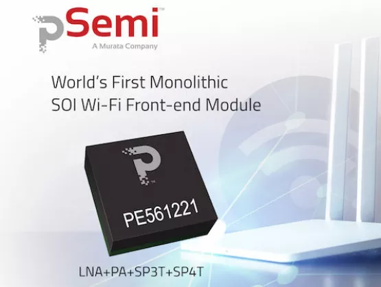
pSemi (formerly Peregrine, now a Murata company) has staked its claim for having the world's first monolithic SOI Wi-Fi front-end module (FEM)—the PE561221. This 2.4 GHz Wi-Fi FEM is the first to integrate a low-noise amplifier (LNA), a power amplifier (PA) and two RF switches (SP4T, SP3T) on a single SOI CMOS die. pSemi says it's ideal for Wi-Fi home gateways, routers and set-top boxes (read the full press release here). Driving this is the new WiFi standard, IEEE 802.11ax, which launches next year. While it's largely meant to tackle issues with WiFi in crowded places, it's also going to be welcome in high-demand home situations. (There's a good piece on the NetworkWorld site on what 802.11ax will do compared to the current 802.11ac – you can read it here). [caption id="attachment_12252" align="alignright" width="300"] The PE561221 uses a smart bias circuit to deliver a high linearity signal and excellent long-packet EVM performance. (Courtesy: pSemi)[/caption] With new standards come new challenges. pSemi explains their PE561221 uses a smart bias circuit to deliver a high linearity signal and excellent long-packet error vector magnitude (EVM) performance. “Traditional process technologies struggle to keep up with both performance and integration requirements, and only SOI can offer the ideal combination of integration and high performance,” says Colin Hunt, vice president of worldwide sales at pSemi. The monolithic die uses a compact 16-pin, 2 x 2 mm LGA package ideal for either stand-alone use or in 4 x 4 MIMO and 8 x 8 MIMO modules. It is based on pSemi’s UltraCMOS® technology platform—a patented, advanced form of SOI that offers superior performance compared to other mixed-signal processes. UltraCMOS technology also enables intelligent integration, notes pSemi—the unique design ability to integrate RF, digital and analog components on a single die. Volume-production parts and samples of the PE561221 are now available from pSemi. And this is just the beginning: while the PE561221 is the first product in the pSemi Wi-Fi FEM portfolio, the product roadmap includes 5 GHz Wi-Fi FEM solutions. The folks at pSemi have been doing RF-SOI for 30 years now, and recently shipped their 4 billionth chip. For the last five years, they've partnered with GlobalFoundries.
Read More
FD-SOI was a very important topic during the recent Mount Qingcheng China IC Ecosystem Forum. To situate things, Mount Qingcheng, with its lush hills and waterways, is located just outside of Chengdu. That of course is where GlobalFoundries is building its new fab, which will be the first in China to run FD-SOI. Chengdu is also a key city in China's automotive electronics landscape. [caption id="attachment_12236" align="alignright" width="300"] (Image Courtesy: VeriSilicon)[/caption] The theme of the forum was Building a Smart Automotive Electronics Industry Chain. Over 260 decision-makers from government, academia and industry attended – and the SOI Consortium had a significant presence. The event was chaired by Wayne Dai, CEO/Founder of consortium member VeriSilicon, and tireless champion of the the FD-SOI ecosystem in China and worldwide. Morning keynotes were given by: Carlos Mazure, Soitec CTO and SOI Consortium Executive Co-Director; Mark Granger, GF's VP of Automotive Product Line Management; and Tony King-Smith, Executive Advisor at AImotive, a GF 22FDX customer. BTW, transcripts of all the talks are available through Gasgoo, China's largest automotive B2B marketplace. You can click here to access them. (They're in Chinese – but you can open them in the language of your choice using the major translation websites.) Chengdu Officials Affirm Support for FD-SOI Fan Yi, Deputy Mayor of Chengdu, spoke extensively of FD-SOI in his keynote on the importance of rapidly developing smart cars. He heralded the “spectacular” new GlobalFoundries fab there. Following a meeting with the company's top brass the day before, he affirmed GF's confidence in their investment. There is a solid roadmap for FD-SOI, he noted, and efforts are underway to accelerate the move into production and expand education and training. He cited the benefits of FD-SOI for the entire supply chain, from design through package and test, raising the level of the entire IC industry to new heights. The government, he said, attaches great importance to this enterprise. Their thinking regarding intelligent transport in China is integrated with the overall approach to smart cities. SOI Consortium Leads Industry Keynotes [caption id="attachment_12232" align="alignleft" width="300"] Wayne Dai, VeriSilicon Founder and CEO (Photo courtesy VeriSilicon)[/caption] In his opening remarks, Wayne Dai emphasized the need for China to seize the advantage in the next round of development opportunities in the automotive electronics industry. This year's Qingcheng forum, he noted, brought together key representatives from across the supply chain, from of the highest to the deepest reaches of the smart car electronics industry, and across markets, technologies, solutions, industrial ecosystem, standards and regulations. In his talk on how FD-SOI is boosting the accelerated development of automotive electronics, Carlos Mazure presented the SOI Industry Consortium. He noted that the Consortium promotes mutual understanding and development across the ecosystem. SOI is already present throughout automotive applications, he noted. There are currently about 100mm2 of SOI per car, in such diverse areas power systems, transmissions, entertainment, in-vehicle networking and more. SOI will experience especially high growth in electrification, information/entertainment, networking, 5G, AI/edge computing and ADAS. He then went on to give some history and an extensive overview of the major trends and highlights we've seen over recent years. He finished by giving examples of convergence across the supply chain with IC manufacturers working with automakers to lower power, increase processor performance and advance 5G. [caption id="attachment_12233" align="alignright" width="665"] Carlos Mazure, Soitec CTO and SOI Consortium Executive Co-Director; Tony King-Smith, Executive Advisor at AImotive and Mark Granger, GF's VP of Automotive Product Line Management (Photo courtesy VeriSilicon)[/caption] GF's Mark Granger addressed the rapid development of automotive electronics. In certain areas, he said, he sees growth rates of over 20%. They are working on building the Chengdu ecosystem, especially for design, and in cooperation with the rest of the supply chain. Furthermore, he reminded the audience, when you talk about cars, travel implies that you also talk about IoT as well as things like infotainment and integrated radar ICs. In addition to cost and power efficiencies, the AEC-Q100 standard for IC reliability in automotive applications is also pushing designers to turn to FD-SOI. In the GF meeting with Chengdu government officials (referenced above in deputy mayor Fan Yi's talk), he too confirmed their support of FD-SOI as a key technology for China. GF is currently cooperating with about 75 automotive partners, he said, and the company is looking to increase cooperation with partners in the Chengdu region. Tony King-Smith talked about the 22FDX test chip AImotive is doing with Verisilicon and GF. In case you missed it, in June 2017 AImotive announced its AI-optimized hardware IP was available to global chip manufacturers for license. AiWare is built from the ground up for running neural networks, and the company says it is up to 20 times more power efficient than other leading AI acceleration hardware solutions on the market. In the same announcement, they revealed that VeriSilicon would be the first to integrate aiWare into a chip design,and that aiWare-based test chips would be fabricated on GF's 22FDX. The chip is expected to debut this year. While the afternoon agenda was not specific to FD-SOI, it did focus on the "smart cockpit" and "intelligent driving", with talks by nine leading players in China's automotive IC and investment communities. ~ ~ ~Note: Many thanks to the folks at VeriSilicon, who wrote up this event for their WeChat feed, and shared photos with us here at ASN.

Read More
IntroductionStarting July 4, 2022, PFOA (Perfluorooctanoic acid) levels in semiconductor manufacturing and related equipment (SMRE), including replacement parts, entering the European Union (EU) will be restricted to 25 ppb per component (or any part thereof). Semiconductor equipment components (and the parts thereof) of particular concern include fluid tubing and fittings, pipe/seal tape, wire and cable insulation, filters, valves, tanks, panels, reaction vessels and o-rings; if they are made from fluoropolymers or fluoroelastomers.When PFOA is used as an aid to the manufacture fluoropolymers such as PTFE, PFA, PVDF or fluoroelastomers such as FKM and FFKM (collectively referred to as fluoromaterials), an unintended PFOA residue can be trapped within the fluoromaterial. Buyers of components used in SMRE are usually unaware of the processing method used for any fluoromaterials they may contain, and, as a consequence, the potential for PFOA residue. This lack of information about potential PFOA residues could result in regulatory enforcement actions and restricted market access, particularly in the EU.The impact of restrictions on fluoromaterials used in SMRE has been introduced in previous SEMI articles ‘Fluorinated Compound Restrictions May Trigger Costly Equipment Changes’ and ‘Fluorinated Substance Restrictions Triggers Costly Equipment Changes.’PFOA and its related compounds, such as the ammonium salt APFO (collectively called PFOA in this article), are recognized internationally as hazardous chemicals and are now targeted for regulatory restriction in the U.S., Taiwan, Canada and the EU. The UN Stockholm Convention on Persistent Organic Pollutants (POPs) is also considering listing PFOA, which could lead to additional international restrictions.The SEMI EHS Division PFOA Compliance Working Group has been working to understand: The likelihood of PFOA residue entering the supply chain of new components The residual level of PFOA in fluoromaterials produced prior to the phase out of PFOA by some manufacturers The impact of PFOA residue on the secondary equipment market This SEMI resource page, ‘Elimination of PFOA from the Equipment Supply Chain,’ and the supporting FAQ contain the Working Group’s key findings and conclusions.PFOA in the Fluoromaterial Supply ChainSignatories to the U.S. EPA Stewardship Program, which include FluoroCouncil members, eliminated PFOA from their manufacturing processes by 2013. However, other fluoromaterial manufactures – particularly in China, Russia and India – might still use PFOA and pose a significant risk to the worldwide supply chain.China, the world’s largest fluoromaterial producer, accounts for 53 percent of global production of PTFE and 38 percent of worldwide production of PVDF, FEP and FKM. An estimated 75 percent to 85 percent of fluoromaterials are manufactured using PFOA in China. Fully 25 percent of these fluoromaterials are exported, primarily to the U.S, Japan, EU and India. What’s more, finished goods made from or containing fluoromaterials that might be used as components in SMRE are exported from China.Documentation that traces fluoromaterials through the supply chain back to the original fluoromaterial manufacturer is key to meeting the PFOA regulatory requirements. This traceability can be straightforward in cases when an SMRE manufacturer directly specifies the use of a fluoromaterial in a custom-fabricated fluoromaterial component. However, for off-the-shelf components (e.g., cable ties, wiring insulation, tubing) or the components assembled from these components (e.g., controllers), the complexity and dynamics of the supply chain makes traceability back to the original fluoromaterial producer almost impossible.Residual PFOA Levels If, or how much, PFOA/APFO residue is contained in a fluoromaterial depends on the manufacturing process. Details of the manufacturing processes are proprietary and vary widely. Post manufacturing thermal treatments, such as sintering, extrusion, and molding, can result in the rapid thermal decomposition of APFO above 250C, but PFOA is significantly more stable. The temperature and time of thermal treatments is also proprietary and varies depending on the type of fluoromaterial and what is being made.This variability makes it impossible to estimate the likely level of trapped PFOA or APFO in a finished component or a part thereof. It is unwise to use data on the level of residue made known for one case to extrapolate the level of residue across the fluoromaterial industry. However, an industry-wide range on the order of 1ppm-10ppm (nearly 1000 times the EU limit) is suspected. Testing for the presence of PFOA/APFO at 25ppb in components is also problematic as there is no standard test method, and results among the custom methods developed in each test lab may vary.Given this uncertainty in test methods, a system of supplier declarations warrants consideration.Impact on Secondary (Used) EquipmentThe EU REACH restrictions apply to SMRE and replacement parts placed on the market at any time (not just initial placement – known as “first placing on the market”). For fluoromaterial components manufactured prior to 2013, there is a higher likelihood of residual PFOA/APFO levels exceeding the 25ppb limit of EU REACH. In principle all the SMRE components containing fluoromaterials should be investigated, and those containing PFOA above 25ppb must be replaced before the SMRE can be legally placed again on the EU market. Companies (e.g., semiconductor manufacturers) in the EU who wish to sell used equipment within the EU will be required to demonstrate the used equipment is in compliance. Selling older used equipment would likely be unprofitable after necessary investigations and component replacements are completed.Next StepsWhile the EU semiconductor manufacturing industry heavily depends on the secondary (used) equipment market, EU regulators may be unaware of the PFOA restriction’s damaging impact to this market. The EHS Division PFOA Working Group, in conjunction with SEMI Europe, is now considering how to bring this concern to the attention of regulators and to collaborate and lobby for effective changes including possible modifications to the EU Persistent Organic Pollutants (POPs) regulation.
Read More
Ahead of his presentation on the future of wearables at the European MEMS Sensors Summit 2018, 19-21 September in Grenoble, France, SEMI spoke with Dr. Peter Weigand, vice president, Business Strategy and Portfolio Management, Bosch Sensortec GmbH. Dr. Weigand gave a glimpse into insights he’ll share at the event.1. Wearables such as smartwatches, fitness trackers or hearables are becoming ubiquitous – but what are the must-haves for wearables for daily use by wearers?We see that users nowadays want to track their activities such as steps walked, calories burnt and floor levels “climbed” on a daily and holistic basis. “Quantifying yourself” is becoming an overall trend in our society with health, fitness and well-being continuously gaining in importance. This is only possible if information about activities is delivered comprehensively in an accurate manner. Therefore, at Bosch Sensortec we provide MEMS sensors that measure the user’s activity very precisely. For example, the smart sensor hubs BHI260 and BHA260 provide sophisticated in-sensor algorithms (e.g. activity recognition) with very low latency and guaranteed performance due to the real-time nature of the embedded software. From the system manufacturer’s perspective, “quantifying yourself” on a 24/7 basis means that the device has to be “always-on.”However, these always-on functions usually consume a lot of battery power, which poses challenges to the manufacturers and system designers, as the battery capacity is usually small due to the size of the wearable. This shows two other must-haves for the users nowadays. First, the compact size of the device. While smartphones have become larger, users of wearables benefit from the devices’ small size and their low weight, offering the possibility to wear them directly on the body. Therefore, we design the footprint and height of our MEMS sensors as small as possible to ensure the compact size and the ease of integration into new, stylish types of wearables. For example, the BMP388, measuring only 2 x 2 x 0.75 mm³, qualifies as the world’s smallest barometric pressure sensor. The second requirement in this regard is long battery life. Users do not want to charge their wearable device every other day, as this would also impede the always-on activity tracking aspect. At Bosch Sensortec, we hence provide MEMS sensors that run at ultra-low power to ensure always-on endurance and a long battery life. The BMA400 is an ultra-low power acceleration sensor that draws ten times less current than existing accelerometers.2. Are there any other user requirements for wearables?Yes, we see for example that just tracking the number of steps or the calories burnt is not enough anymore. Users require multi-functional devices that also provide information that can be used to monitor sleeping behaviour, navigate in cities, or prepare your smart home for your arrival. We are equipping our sensors with more features and developing new types of sensors that add new functionalities to wearable devices. For example, we have developed a smart watch Projection Module that can project information on the back of the user’s hand for an additional, enlarged display. While smart watches are rising in popularity, demand for basic wristbands is waning. Users are paying more attention to device design. Like clothing, the look and feel of the device should support the user’s individual style.At the same time, with more fashion brands are entering the wearables market we are providing sensors that are easy to integrate into new types of wearables such as hybrid watches. Our products feature a small form factor to ensure flexible, simple design-in. For example, the new BMA400 acceleration sensor easy to design into various applications. Finally, to conform to the user, the wearable must adapt to the user’s individual habits and motions such as learning different gestures, requiring the devices to be not only smart but increasingly intelligent with artificial intelligence (AI). We are providing sensors, such as the BHI260, with embedded, local intelligence with advanced algorithms that enable devices to learn. We are developing intelligent software solutions that use deep learning, enabling device to adapt to the user’s individual behaviour.3. What current techniques are design engineers using to reduce power consumption of wearables?Several techniques are being developed to reduce power consumption. The goal largely is to reduce the power draw of components that are always-on, such as the screen in a smartwatch. In activity trackers, the motion sensor is always on to sense, track, classify and store motion data. Reducing the power needed to operate these features will cut total system power consumption as well. A good example is our BMA400 accelerometer that has a current consumption of less than 1 µA in full operation.At the same time, it independently processes sensor data. For example, the device converts the three-axis motion sensor data stream into step counting events. This allows the main (host) microcontroller to remain in the stand-by mode required for activity tracking and to be activated by the accelerometer to deliver full power only, say, every 100 steps. The sensor, rather than the microcontroller, manages the overall duty cycling of the microcontroller to reduce system power and increase overall efficiency.4. What alternatives are engineers exploring to reduce power consumption? What is the role of intelligence directly within sensors for local processing capabilities in wearables?We have seen how the BMA400 can reduce power by integrating the motion classification functions. We can take this concept further by integrating a microcontroller that’s specifically tailored for low-power sensor data processing, such as the “fuser core” that Bosch Sensortec uses within its smart sensor hubs such as BHI260 or BHA260. The built-in sensor data fusion and machine learning hardware accelerators make it uniquely suited to reduce overall system power. The concept of edge computing has been around for many years, but only in this and the previous sensor generation with built-in local intelligence are we reducing the full power profile of the wearable device. Our sensor architecture design allows us to process the power locally in the MEMS sensor without waking up the main application processor.5. What technologies are you developing to lengthen battery life without compromising performance? We are continuously improving the MEMS and ASIC designs of our sensor portfolio to drive ever higher power efficiency. The BMA400 draws 10 times less current than existing accelerometers while delivering solid high performance (e.g. low-noise data). 6. Wearable device feature and performance requirements are continuously rising. Will batteries need to be larger to support these requirements? Since the beginning of the portable consumer electronics, improving batter life and reducing chip power consumption have been parallel efforts, a trend we expect to continue. However, we expect a greater focus on the overall system power reduction with sensors managing the power, turning on and off microcontrollers, radios (including GPS) and displays in wearable devices.7. What do you expect from European MEMS Sensors Summit 2018 and why do you recommend attending in Grenoble?The European MEMS Sensors Summit is a very important platform for us. It is an opportunity to meet partners, customers, industry leaders, to exchange ideas and to get new insights and thus to ultimately refine our solutions for our global customer base. Our ultimate goal is to improve people’s individual lifestyle and well-being.Serena Birschetto is a marketing communications manager in SEMI Europe.
Read More
Intento Design is working with STMicroelectronics to bring ID-XploreTM EDA software, which is aimed at solving the critical analog design challenges, to FD-SOI process nodes. “ID-Xplore is a disruptive EDA software that accelerates analog design and migration processes by at least one order of magnitude. It reduces the cost and latency inherent to analog design. Currently, there is no similar EDA tool on the market covering the analog design challenges like ID-Xplore,” noted Dr. Ramy Iskander, CEO of Intento Design (see the press release here). ST's FD-SOI design expertise roots, of course, are as deep as they get. “ST’s decision to work with us confirms the relevance of our solution. We are very excited to work jointly with ST teams to take the most benefit out of FD-SOI technology leveraging ST’s pioneering leadership in this area,” continued Dr. Iskander. “We’ve already seen the benefits of ID-Xplore in accelerating the design phase of different analog circuits, thanks to the software’s fast and accurate exploration capabilities in advanced FD-SOI processes,” said Thierry Bion, ST's Hardware Design Director, Aerospace Defense Legacy Division. “By facilitating IP reuse and sharing of design insights between engineers, ID-Xplore™ is helping our teams significantly accelerate new product introductions.” ID-Xplore uses the OpenAccess database standard and is fully integrated within the Cadence design environment. The designer’s implicit and explicit knowledge is expressed as technology-independent constraints, bringing the designers back to their core expertise and creativity. If you want to learn more, the folks over at semiwiki.com have made a number of posts on Intento Design recently. They're really helpful in understanding what the company does, how and why: CEO Interview: Ramy Iskander of Intento Design Edit (by Daniel Nenni) – good backgrounder on the company and product. The Intention View: Disruptive Innovation for Analog Design Edit (by Daniel Nenni) – an excellent interview with Dr. Caitlin Brandon about how the tool works and how it aligns with and supports the way analog designers work. A New Kind of Analog EDA Company Edit (by Daniel Payne) – Daniel Payne started his career as a circuit designer at Intel, and is now a well-known consultant/expert in the EDA world. Here he explores how ID-Xplore actually works and its “cool new automation features”.
Read More
Specialty foundry TowerJazz is ramping a 65nm version of its RF-SOI process on 300mm wafers at Fab 7 in Uozu, Japan. To support the ramp, the company has signed a contract with long-term partner, Soitec, guaranteeing a supply of tens of thousands of 300mm SOI silicon wafers, securing wafer prices for the next years and ensuring supply to its customers, despite a tight SOI wafer market. [caption id="attachment_12108" align="alignright" width="300"] The 300mm 65nm RF-SOI process will be offered at the Uozu, Japan fab, which is operated by the TowerJazz Panasonic Semiconductor Company (TPSCo). (Photo courtesy: TowerJazz)[/caption] Five of TJ's seven fabs do RF-SOI. LNA (low-noise amplifers) are a big market driver, and with RF-SOI they can integrate the LNA with the switch, CEO Russell Ellwanter said in his lead keynote at the SOI Consortium’s 5th International RF-SOI Workshop in Shanghai (spring, 2018). BTW, that was in fact a very inspirational talk about Value Creation, and the importance of treating your suppliers with respect. He credited his company’s close relationship with RF-SOI wafer-supplier Soitec for TJ’s claim to the world’s best linearity. “We are delighted to see the strong adoption of 300mm RF SOI through this large capacity and supply agreement with TowerJazz to augment our already significant 200mm RF-SOI partnership,” said Soitec CEO Paul Boudre. “TowerJazz was the first foundry to ramp our RFeSI products to high volume production in 200mm and continues as one of the industry leaders in innovation in this exciting RF market with advanced and differentiated offerings.” According to the TJ press release (you can read it here), with its best in class metrics the TowerJazz 65nm RF-SOI process enables the combination of low insertion loss and high power handling RF switches with options for high-performance low-noise amplifiers as well as digital integration. The process can reduce losses in an RF switch improving battery life and boosting data rates in handsets and IoT terminals. It's a high-growth market, to be sure. Market researchers Mobile Experts predict that the mobile RF front-end market will reach $22 billion in 2022 from an estimated $16 billion in 2018. TowerJazz says its breakthrough RF SOI technology continues to support this high-growth market and is well-poised to take advantage of next-generation 5G standards, which will boost data rates and provide further content growth opportunities in the coming years. Customers are already getting into position. For example, Maxscend (WuXi, China), a provider of RF components and IoT integrated circuits, is ramping in this new technology. “We chose TowerJazz for its advanced technology capabilities and its ability to deliver in high volume while continuously innovating with a strong roadmap. We specifically selected its 300mm 65nm RF SOI platform for our next-generation product line due to its superior performance, enabling low insertion loss and high power handling,” said Maxscend CEO Zhihan Xu. As longtime ASN readers will know, we've been covering the evolutions of TJ's RF-SOI platforms since the beginning of the decade. It's worth noting, too, that beyond RF, TowerJazz also offers foundry customers other SOI-based processes, such as the new 0.18μm BCD SOI, a 200V SOI technology platform (announced in 2017, press release here) for motor drivers, industrial tools, electric vehicles and more. The previous generation 0.18μm SOI for automotive power management also offers exceptional area savings and is well-suited for high temperature operation. Back in 2014, here at ASN we did a great interview with TJ SVP Dr. Marco Racanelli about when and why they use SOI – and while processes have advanced, the basic drivers are still there, so it's a still a good read. And finally, designers will want to know that the TJ Multi-Project Wafer (MPW) Shuttle Program offers the 65nm RF-SOI process, as well as other SOI-based processes. See the website for scheduling and details.
Read More
GlobalFoundries has announced that the company’s 22nm FD-SOI (22FDX®) technology has delivered more than two billion dollars of client design win revenue. With more than 50 client designs, 22FDX is being used in power-optimized chips across a broad range of high-growth applications such as automotive, 5G connectivity and IoT. Their clients chose it for the significant reductions in power and die size relative to a traditional bulk CMOS process, says the company. 22FDX offers the industry’s lowest operating voltage, delivering up to 500MHz frequencies at only 0.4 volts. The technology also delivers efficient single-chip integration of RF, transceiver, baseband, processor, and power management components, “...providing an unparalleled combination of high performance RF and mmWave functionality with low-power, high density logic for devices that require long-lasting battery life, increased processing capability, and connectivity.” 22FDX is in early production, with yields and performance matching client expectations. A recent VLSI Research survey indicated that FD-SOI technology is seen as a complementary technology to FinFET. It's gaining traction in application spaces such as IoT, where power consumption is important and the product life is relatively short. “We’re only just beginning,” said GF CEO Tom Caulfied. “We have found a way to separate ourselves from the pack by emphasizing our differentiated FD-SOI roadmap and client-focused offerings that are poised to enable connected intelligence. We will continue to build on our momentum and look for ways to expand our reach to address the evolving needs of the industry.” Here's a sampling of customer quotes from the press release (read more here): “At Synaptics, as we expand upon our industry-leading mobile and PC businesses to include delivering new and innovative products that address the booming IoT market, we require the best available technologies to enable us to deliver top-notch solutions including voice and multimedia processing capabilities for our customers,” said the company's CEO, Rick Bergman. “GF’s 22FDX technology delivers a potent mix of low static and dynamic power along with excellent performance to give us a great platform for our world-class products.” “As our customers increasingly demand more from their mobile experiences, our partnership with GF on its 22FDX technology is critical to differentiate ourselves in the competitive market and deliver powerful and efficient mobile SoCs,” said Rockchip CEO Min Li. “Our goal has always been to provide more secure, connected experiences for drivers. Combining our leadership in radar technology with GF's 22FDX automotive-qualified process, we are able to deliver a cost-effective, high performance, low power solution that opens new opportunities for car manufacturers to provide better experiences for drivers around the world," said Kobi Marenko, CEO of Arbe Robotics. “The automotive industry realizes that assisted driving solutions require more camera information besides Radar and Lidar, integrating information from multiple cameras. The resulting DreamChip multi-core vision processor platform, based on the 22FDX process is providing European auto makers and Tier 1 automotive component suppliers with a platform from which they can create custom derivatives with a massively reduced time to market," said Dream Chip Technologies CEO Jens Benndorf. “With 22FDX, the value proposition for us is the potential power and area savings, two key metrics for our highly optimized LTE NB-IoT and CAT-M chipsets. In addition, leveraging the growing ecosystems of IP available in the 22FDX process helps to accelerate time to market,” said Peter Wong, CEO at Riot Micro, which designs purpose-built silicon for wireless IoT applications. (Read more about that here.) GF adds that it is preparing to deliver 12FDX™ technology, which will provide a full node scaling benefit and improved power efficiency for a new generation of applications, from edge-node artificial intelligence and AR/VR to 5G networking and ADAS.
Read More