downloadGroupGroupnoun_press release_995423_000000 copyGroupnoun_Feed_96767_000000Group 19noun_pictures_1817522_000000Member company iconResource item iconStore item iconGroup 19Group 19noun_Photo_2085192_000000 Copynoun_presentation_2096081_000000Group 19Group Copy 7noun_webinar_692730_000000Path
Skip to main content
Default Banner Image

Technology and Trends

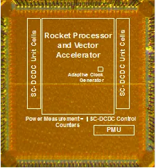
ST Fellow Dr. Andreia Cathelin gave a terrific presentation at the recent CMP Annual Meeting. Now posted and freely available, Performance of Recent Outstanding 28nm FD-SOI Circuits Taped Out Through CMP highlighted eight examples – though she told ASN that she had easily over 50 from which to choose.CMP is a Multi-Project Wafer (MPW) service organization in ICs, Photonic ICs and MEMS. They’ve been organizing prototyping and low volume production in cooperation with foundries for over 37 years. In partnership with ST since 1994, in the fall of 2012 they opened access to MPW runs in the 28nm FD-SOI process. More than 180 tape-outs have been fabricated since then using the process.As Dr. Cathelin said, this lets ST show their industrial clients just how good the technology is. The chips she chose to cover in her presentation get “spectacular performance”, she said, especially for low-power or power-sensitive SoCs.Here’s a quick recap of what she presented (some of which she co-authored), followed by some other SOI-related updates from the CMP meeting.8 (of Many) Great ChipsFD-SOI, said Dr. Cathelin, “...is unmatched for cost-sensitive markets requiring digital and Mixed Signal SoC integration and performance.” In the first dozen slides of her presentation, she gave the technical details on the advantages of FD-SOI in analog, RF/millimeter wave, Analog/Mixed-Signal and digital design. If you're a designer, you'll want to check those out.Then she ran through eight great chips – all manufactured by ST on 28nm FD-SOI through CMP's MPW services. Here they are. (You can click on the illustrations to see them in full screen.)1. A digital delay line with coarse/fine tuning through gate/body biasing in 28nm FDSOI [caption id="attachment_11559" align="alignnone" width="768"] (Courtesy: CMP, ST, ISEN)[/caption] This chip was presented at ESSCIRC '16 by a team from ISEN Lille, Professors Andreas Kaiser and Antoine Frappé (you can get the complete paper by I.Sourikopoulos et al on IEEE Xplore – click here.) As noted in the abstract, “Delay controllability has always been the major concern for the reliable implementation of circuits whose purpose is timing.” By leveraging body biasing in FD-SOI, this novel low-power design architecture for 60GHz receivers enables very high bandwidth together with fine-grain wide range delay flexibility, for implementing Delay Feedback Equalizer techniques in the Intermediate Frequency (IF) reception path. The results are state-of-the-art: ultra wide range, linear control, fs/mV sensitivity and energy efficient controllable delay cells. 2. 28FD-SOI Distributed Oscillator at 134 GHz and 202GHz [caption id="attachment_11560" align="alignnone" width="768"] (Courtesy: CMP, ST, ims)[/caption] Presented at RFIC '17 by a team from the IMS Bordeaux lab, Professor Yann Deval and STMicroelectronics, this chip demonstrates the highest oscillation frequency attainable so far at the 28nm node, be it planar bulk or FD-SOI. (Click here to get the full paper by R. Guillaume et al from IEEE Xplore.) As noted in the abstract, solutions on silicon for mmW and sub-mmW applications have been demonstrated for high-speed wireless communications, compact medical and security imaging. The main challenges are for the signal generation at high frequencies, and this implementation demonstrates spectacular oscillation frequencies close to the transistor’s transition frequency (fT). In this chip, they used body bias tuning to optimize the phase noise, demonstrated very low on-wafer variability, and simulation methods that permit measurement prediction precision within 0.1%.3. A 128 kb Single-Bitline 8.4 fJ/bit 90MHz at 0.3V 7T Sense-Amplifier-less SRAM in 28nm FD-SOI [caption id="attachment_11561" align="alignnone" width="768"] (Courtesy: CMP, ST, Lund U.)[/caption] Extremely energy efficient SoCs are key for the IoT era – but SRAM gets very tricky at ultra-low voltages (ULV). Presented at ESSCIRC '16 by B. Mohammadi et al (on IEEE Xplore here) from Professor Joachim Rodrigues' team at the Lund University, this is a 128 kb ULV SRAM, based on a 7T bitcell. The minimum operating voltage VMIN is measured as just 240mV and the retention voltage is as low as 200mV. FD-SOI enabled them to overcome ULV performance and reliability challenges by letting the Lund U.-lead team selectively overdrive the bitline and wordline with a new single-cycle charge-pump. Plus they came up with a new scheme so it doesn't need a sense amplifier, yet delivered 90MHz read speed at 300mV, dissipating 8.4 fJ/bit-access.4. Matched Ultrasound Receiver in 28FDSOI [caption id="attachment_11562" align="alignnone" width="768"] (Courtesy: CMP, ST, Stanford U.)[/caption] Presented at ISSCC '17 (with an extended relative paper at JSSC '17) by M-C Chen et al with Professor Boris Murmann's team at Stanford, the full title of the paper about this chip is A Pixel Pitch-Matched Ultrasound Receiver for 3-D Photoacoustic Imaging With Integrated Delta-Sigma Beamformer in 28-nm UTBB FD-SOI. (Click here to get it on IEEE Xplore.) It's a a proof-of-concept for a big ultrasound receiver: a “pixel pitch-matched readout chip for 3-D photoacoustic (PA) imaging.” PA is “...an emerging medical imaging modality based on optical excitation and acoustic detection.” It's used in studying cancer progression in clinical research, for example. As noted in the paper abstract, “The overall subarray beamforming approach improves the area per channel by 7.4 times and the single-channel SNR by 8 dB compared to prior art with similar delay resolution and power dissipation.” One of the (many) advantages of FD-SOI in this context is for front-end signal conditioning in each pixel. This unique type of pixel pitch-matched architecture implementation is possible only in a 28nm (or less) node of an FD-SOI technology, as it is matched with the pitch sizing needed for the ultrasound transducers in order to generate signals for a 3-D reading.5. SleepTalker - 28nm FDSOI ULV WSN Transmitter: RF-mixed signal-digital SoC [caption id="attachment_11563" align="alignnone" width="768"] (Courtesy: CMP, ST, UCL)[/caption] Presented at VLSI '16 and JSSC '17 by G. de Streel et al from Professor David Bol’s team at Université Catholique de Louvain la Neuve, the full title of the paper about this chip is SleepTalker: A ULV 802.15.4a IR-UWB Transmitter SoC in 28-nm FDSOI Achieving 14 pJ/b at 27 Mb/s With Channel Selection Based on Adaptive FBB and Digitally Programmable Pulse Shaping (get it on IEEE Xplore here). This chip tackles the IoT requirement for sensing functions that can operate in the ULV context. That means creating wireless sensor nodes (WSN) that can be powered on an energy harvesting power budget – and that's a real challenge if you want to incorporate an RF component that can handle medium data rates (5-30 Mb/s) for vision or large distributed WSN networks. The energy efficiency has to be better than 100 pJ/b. To get there, the UCL-lead team used wide-range on-chip adaptive forward back biasing for “...threshold voltage reduction, PVT compensation, and tuning of both the carrier frequency and the output power. [...] Operated at 0.55 V, it achieves a record energy efficiency of 14 pJ/b for the transmitter (TX) alone and 24 pJ/b for the complete SoC with embedded power management. The TX SoC occupies a core area of 0.93 mm2.”6. A 128x8 Massive MIMO Precoder-Detector in 28FDSOI [caption id="attachment_11564" align="alignnone" width="768"] (Courtesy: CMP, ST, Lund U.)[/caption] This massive MIMO chip was presented at ISSCC '17 by a team from Professors Liang Liu and Ove Edforss at the Lund University in a paper entitled 3.6 A 60pJ/b 300Mb/s 128×8 Massive MIMO precoder-detector in 28nm FD-SOI (H. Prabhu, et al; get it from IEEEE Xplore here). While Massive MIMO (MaMi) will be needed for next-gen communications, it can't be achieved by just scaling MIMO – that would be too costly in terms of flexibility, area and power. As noted in the Lund U. team's intro, “Algorithm optimizations and a highly flexible framework were evaluated on real measured channels. Extensive hardware time multiplexing lowered area cost, and leveraging on flexible FD-SOI body bias and clock gating resulted in an energy efficiency of 6.56nJ/QRD and 60pJ/b at 300Mb/s detection rate.”7. ENVISION: A 0.26-to-10TOPS/W Subword-Parallel Dynamic-Voltage-Accuracy-Frequency-Scalable Convolutional Neural Network Processor in 28nm FDSOI [caption id="attachment_11565" align="alignnone" width="768"] (Courtesy: CMP, ST, KU Leuven)[/caption] Today's solutions for always-on visual recognition apps are an order of magnitude too power hungry for wearables. Running at 10's to several 1OO's of GOPS/W, they use classification algorithms called ConvNets, or Convolutional Neural Networks (CNN). The paper about this chip was presented at ISSCC '17 by a team from professor Marian Verhelst at Katoliek Universiteit Leuven (B. Moons, et al, get it from IEEE Xplore here), and it changes everything. Leveraging FD-SOI and body-biasing, the KU Leuven team solved the power challenge with, “...the concept of hierarchical recognition processing, combined with the Envision platform: an energy-scalable ConvNet processor achieving efficiencies up to 10TOPS/W, while maintaining recognition rate and throughput. Envision hereby enables always-on visual recognition in wearable devices.”8. Fine-Grained AVS in 28nm FDSOI Processor SoC [caption id="attachment_11566" align="alignnone" width="768"] (Courtesy: CMP, ST, UC Berkeley)[/caption] As we learned at SOI Consortium FD-SOI Tutorial Day in SiValley last year, Professor Borivoje “Bora” Nikolic of UC Berkeley is known as one of the world's top experts in body-biasing for digital logic (he and his team have designed more than ten chips in ST’s 28nm FD-SOI!) They presented the RISC-V chip here at ESSCIRC '16 and JSSC '17, in a paper entitled Sub-microsecond adaptive voltage scaling in a 28nm FD-SOI processor SoC (B.Keller, et al, on IEEE Xplore here). As they noted in the intro, a major challenge for mobile and IoT devices is that their workloads are highly variable, but they operate under very tight power budgets. If you apply adaptive voltage scaling (AVS), you can improve energy efficiency by scaling the voltage to match the workload. But in the current gen of SoCs, the AVS timescales of hundreds of microseconds is too slow. The chip the Berkeley team presented brought that down to sub-microseconds by aggressively applying body-biasing throughout the chip, including to workload measurement circuits and integrated power management units. The result is “... extremely fine-grained ( 1μs) adaptive voltage scaling for mobile devices.” (BTW, they expand on some of the details in another paper published in 2017.) These design techniques are now taught at UC Berkeley, as this kind of implementation is the subject of a course in SoC design (including the RF part of transceivers); a first educational chip has already been taped-out and successfully measured. (BTW, Professor Nikolic will once again join Dr. Cathelin and other luminaries in teaching at the SOI Consortium's FD-SOI Training Day in Silicon Valley, 27 April 2018 - click here for sign-up information.)More SOI Through CMPAt the meeting, CMP also made a presentation on all their MPW offerings – you can get it here. On ST's SOI (in addition to 28nm FD-SOI, of course), that includes the new 160nm SOIBCD8s: Bipolar-CMOS-DMOS Smart Power (for automotive sensor interface ICs, 3D ultrasound, MEMS micro-mirror drivers); and 130nm H9-SOI-FEM: Front-End Module (for radio receiver/transceiver, cellular, WiFi, and automotive keyless systems).CMP also provides tutorials that are used by institutions across the globe. A new update to the tutorial, RTL to GDS Digital Design Flow in 28nm FD-SOI Process is now available – you can see the presentation they did about that here. (It now includes LVS and DRC steps with Mentor/Calibre or Cadence/PVS.) Other services, like the 2-day, hands-on THINGS2DO FD-SOI training days at the end of March are always fully booked almost immediately, but don't hesitate to inquire, as they'll be adding more. For some more examples of 28nm FD-SOI chips run through CMP over the years, see their website pages on Examples of Manufactured ICs. There are also some nice examples on pages 21 and 23 of their most recent annual report. For those in the photonics world, CMP has teamed up with Leti to offer Si-310 PHMP2M, a 200mm CMOS SOI platform. CMP is cooperating with Tyndall for the photonics packaging – see that presentation here. Training kits and tutorials will be available in Q3 of this year. And in partnership with MEMSCAP, CMP offers Multi-User MEMS Processes (aka MUMPs) for SOI-MEMS.So lots of terrific SOI resources for CMP – check it out!~ ~ ~Note: special thanks to Andreia Cathelin of ST and Kholdoun Torki of CMP for their help on this piece.

Read More
They've got initial silicon of Dream Chips' ADAS SoC fabbed in GlobalFoundries' 22FDX (FD-SOI) technology, and it's got record power efficiency (read the full press release here). The chip offers high performance image acquisition and processing capabilities and supports AI / Neural Network (NN) vision operation with a total of 1 TOPS at 500 MHz on 4 parallel engines. With all functions including quad-core Arm® Cortex®-A53, Tensilica DSPs, and INVECAS’ LPDDR4-Interfaces activated, the SoC shows single digit power dissipation without the need for forced cooling, which is of significant importance for embedding in automotive environments. [caption id="attachment_11538" align="alignleft" width="277"] Courtesy: Dream Chips Technologies[/caption] Targeting automotive computer vision applications, the SoC was created in close cooperation with Arm, ArterisIP, Cadence, GF, and INVECAS as part of the European Commission’s ENIAC THINGS2DO reference development platform, where about 40 partners in Europe cooperated to propel the FDSOI-Design Ecosystem. Of particular importance is the new and reduced power footprint of this SoC in 22FDX-technology from GF. AI/NN-operation for image recognition is available today, but most of the solutions need active cooling. Implementation of Dream Chip Technologies’ SoC on GF’s 22FDX platform demonstrated single digit Watt and cooling targets for designers managing power dissipation. If needed, the SoC bears the potential to increase the performance even further up to 2 TOPS at 1.0 GHz by applying GLOBALFOUNDRIES’s forward body-bias capabilities and other optimization techniques. The jointly developed ADAS SoC platform from Dream Chip Technologies is available now. Part of GF’s FDXcelerator™ Partner Program, Dream Chip is the largest independent German Design Service company specialized in the development of large ASICs, FPGAs, embedded software and systems with a strong application focus on automotive vision systems (ADAS).
Read More
The solar energy sector shined in a global renewable energy market that maintained steady growth last year despite the United States’ stunning withdrawal from the Paris Agreement. Solar panel costs dropped to an all-time low, driving global demand that surpassed the 100GW mark for the first time on the strength of standout annual 26 percent growth.In 2016, Taiwan began to redouble its transition to renewable energy, most notably phasing out nuclear power as the region increases its reliance on climate-friendly energy sources and seeks more foreign investment, moves it hopes will also boost economic growth and create more jobs.With its land space constraints, the region is fertile ground for rooftop photovoltaic system (PV) systems. So the Taiwan government laid out on ambitious plan to achieve 3,000MW of installed capacity by 2020 – enough to supply electricity for 1 million households while improving air quality, help spruce up the urban landscape and generate jobs.The SEMI Taiwan Energy Group fully backs the government renewable-energy policy. Earlier this year, the group gathered more than 200 industry professionals and government officials to explore challenges and opportunities in deploying more rooftop PV systems. Here are key takeaways from the conference.Infrastructure Reliability Key to High Return on InvestmentSize, reliability and safety are touchstones of rooftop PV system design. To make the best use of space, reduce the cost per kWh, and ensure a long-term, stable supply of electric energy, the PC modules must be: Compact to fit within limited rooftop space Robust to endure extreme temperatures over long periods; resist fire, salt and water damage; and ensure safe, reliable operation Financial Institutions Play Important RoleIn response to the government energy policy, domestic financial institutions have funded select projects or issued bonds and derivative products to support the development of Taiwan’s renewables industry. A key part of these efforts is to evaluate risks in areas such as system module safety, technology and design maturity, energy-generating efficiency and maintenance costs.Circular Economy = Green WorldEnergy storage systems are maturing rapidly to support expanding markets for renewable energy products. Demand for renewable energy systems for homes is growing, fueled in part by low prices, and the adoption of electric vehicles continues to rise as advances in energy storage technology drive down costs and enable longer ranges. At the current pace of technology development, the world could be using 100 percent renewable energy as soon as 2025. However, a pollution-free environment will only be possible with the development of a circular economy – one that regenerates and reuses energy resources. To that end, the SEMI Taiwan Energy Group this year will transform the 11-year-old PV Taiwan exhibition into Energy Taiwan, Taiwan’s largest international platform for facilitating communication and collaboration of the entire renewable energy ecosystem. Exhibition themes will range from solar energy, wind energy, hydrogen energy and fuel cells to green transportation, smart energy storage and green finance. The event reflects the consolidation of the SEMI Taiwan Energy Group’s growing resources and its commitment to a circular economy free of fossil fuels.Emmy Yi is a senior marketing specialist at SEMI Taiwan.
Read More
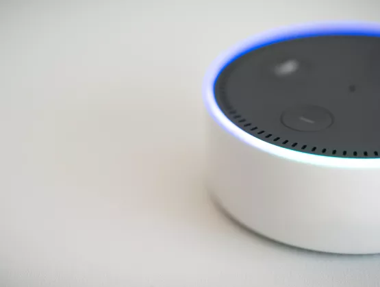
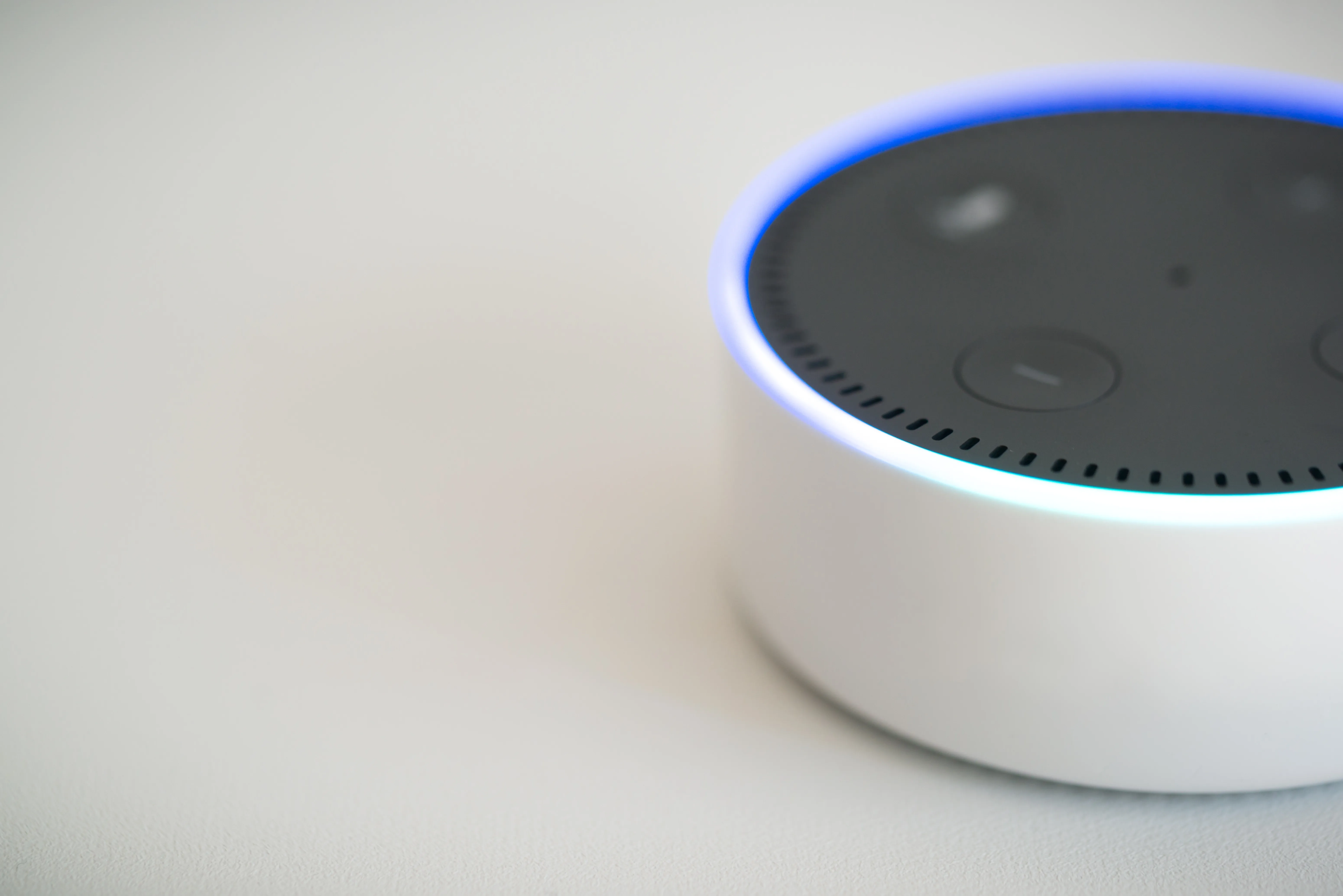
Smart speakers and voice assistants are already a big part of everyday life for many of us. Improvement in speech recognition accuracy obtained from advancements in natural language processing, machine learning and cloud computing technologies is driving the success of voice assistants. We’re asking Siri to play music, Alexa to order kitchen supplies and OK, Google for the weather. The world’s largest consumer electronics tradeshow, CES, was monopolized by voice assistants this year.But what’s behind the smart speakers? Even smarter microphones. There are two different kinds of tiny microphones in our smart devices, including smartphones, smart home products and smart speakers – capacitive and piezoelectric MEMS (microelectro-mechanical systems) microphones. MEMS microphones offer high signal-to-noise-ratio (SNR), low power consumption, good sensitivity, and are available in very small packages that are compatible with surface mount assembly processes, according to EDN Network. Capacitive MEMS microphones have been the industry standard for 50 years, until recently. A new player hit the scene in the last couple of years – the piezoelectric MEMS microphone.Piezoelectric MEMS microphones are transforming the capabilities of smart speakers by offering better far-field performance, ruggedness and extreme durability over time. In fact, piezoelectric MEMS mics from Boston-based Vesper Technologies, for example, are natively immune to environmental contaminants such as dust, water, humidity, oil and even beer. Piezoelectric MEMS microphones offer significant power savings over battery-powered smart speakers compared to capacitive-based “always on, always listening” solutions. That means that the microphone is absorbing virtually no power until it’s turned on by a “wake word” such as “Hey Siri.”Another crucial advantage of piezoelectric MEMS comes from the inherent linearity of piezoelectric transduction that can withstand extreme sound pressure levels without saturating the microphones. What this means to smart speakers is that the audio quality, particularly the bass response, on the speakers need not be compromised to avoid saturation of microphones in music barge-in scenario. From a consumer perspective, this feature translates to higher wake-word detection accuracy without compromising on audio quality while playing music at loud volume levels. All of these advantages when integrated into microphone arrays lead to improved speech recognition accuracy and consistent long-term performance, a rare combination we think is best achieved with piezoelectric microphones.These different types of sensors can significantly increase the utility rates of smart speaker products in a household, a major challenge that smart speaker developers are trying to solve. Imagine a smart speaker that can interact and move along with you to teach yoga or an Echo Dot in your bedroom that can seamlessly communicate the temperature and/or humidity level to a thermostat without any user interaction. While motion sensors can help create an emotional bond with the user, environmental sensors on-device can offload some of the communication to the cloud or another IoT hub, thereby reducing the latency and power consumption. Some of these features are currently only limited to highly priced niche products, but one can expect the proliferation of these devices into the mass market in the years to come.Amazon’s first-mover advantage resulted in its large market share within the smart speaker segment. Alexa Voice Services’ growing third-party integrations and rapidly evolving ecosystem of connected smart home services indicate a strong foothold for Amazon. Information plays a key role in the race for marketshare in these connected services, and MEMS/sensors are at the forefront of this information-gathering process. Adoption of a wide variety of sensors, including technologies such as piezoelectric MEMS sensors, can provide significant value and competitive advantage in data science.Matt Crowley is CEO of Boston, MA-based Vesper Technologies
Read More
Since 2010, 474 companies worldwide have poured $51 billion into developing artificial intelligence (AI) devices, with the bulk of these investments targeting autonomous driving and in-vehicle experiences, according to a McKinsey Company report. With the extraordinary growth potential of AI and automotive electronics, it’s no surprise that IHS Market predicts the Advance Driver Assistance Systems (ADAS) market will reach $67.43 billion by 2025. By 2040, the market research firm expects 33 million autonomous vehicles enabled by AI to be on the road worldwide. Lured by the immense business opportunity, more semiconductor manufacturers are jumping into the automotive market knowing that autonomous driving ICs will face far more stringent reliability requirements than traditional devices. Testing, then, will be crucial for level 5 autonomous driving to materialize since a fully autonomous system will need to rival the behind-the-wheel performance of a human driver even in extreme road conditions like snow and iceWith testing vital to the development of chips for autonomous driving, SEMI Taiwan recently convened experts from IC design and testing-related fields to facilitate cross-discipline collaboration and help inspire innovative solutions to current testing challenges. The early February AI IC and Automotive IC Test Seminar is part of a series of SEMI Taiwan events focused on hot topics including like AI, IoT, smart automotive, smart data and smart MedTech. Following are a key takeaways from the seminar.Paradigm Shift Needed in Automotive Electronics Testing StrategiesDesigners of automotive electronics need to transform their test strategies to match the technical rigors of autonomous driving. The traditional process of build, test, and then fix-for-compliance must change in the era of self-driving vehicles. Adding AI to already electronically complex automotive systems will dramatically increase the number of ICs and sensors in vehicles. Traditional component testing for points of failure is far less rigorous than vetting devices under the countless driving scenarios where they could fail. Testing, therefore, must be holistic. Starting in the development phase of their own electronics systems, automotive electronics designers must work closely with component and other technology suppliers to ensure that designs are tightly integrated and exhaustively tested for interoperability and points of failure under any conditions a human driver would face. Wafer-level Test is A TrendThe cost and time for IC testing have steadily increased to meet the relentless scaling requirements of highly integrated advanced technologies, placing immense pressure on current wafer-level packaging and testing methodologies to maintain cost efficiencies, chip yields and time-to-market speed. The challenges will intensify with the multiple-component parallel testing required for autonomous vehicles. Demands on automotive electronics manufacturers to maintain DDPM quality levels key to smart functionalities, powertrain operation, safety and reliability will also complicate current IC testing methodologies. Nearly 300 professionals from IC design and related fields gathered at the SEMI Taiwan forum to tackle the challenges of autonomous vehicle testing Beyond TechnologyTo fulfill the promise of autonomous automobiles and other AI applications, industry, academia, and government in Taiwan must work together to solve underlying technical challenges, create profitable business models and develop a strong programming and system integration workforce. Taiwan's strong semiconductor manufacturing industry and advanced IC testing capabilities put it in the pole position to help drive the development of advanced automotive electronics essential for autonomous vehicles.Emmy Yi is a senior marketing specialist at SEMI Taiwan.
Read More
FD-SOI has hit Q1 with terrific momentum, both in terms of visibility into products and in press coverage. In case you missed them, here are three articles you should definitely read: FD-SOI Adoption Expands – Technology shifts direction after years of competing directly with CMOS at advanced nodes (by Ed Sperling at Semiconductor Engineering) 22FDX Shows IoT Traction at MWC 2018 (by David Lammers for GF's Foundry Files) The Future of Silicon: An Exclusive Interview with Dr. Gary Patton, CTO of GlobalFoundries (by Ian Cutress at AnandTech) But, if you don't have time to read them all right away, here are some highlights to tide you over til you do. Expanding Adoption Ed Sperling at SemiEngineering sees FD-SOI adoption “... gaining ground across a number of new markets, ranging from IoT to automotive to machine learning, and diverging sharply from its original position as a less costly alternative to finFET-based designs.” After recounting the advantages (with which ASN readers are well familiar), he notes that two things have changed in our industry. First, fewer and fewer companies can afford to design in the most advanced FinFET nodes. And second: there are enough emerging markets where power is critical, but there won't necessarily be the billions of units per chip needed to amortize exorbitant design costs. In particular, for FD-SOI adoption he cites, “...the inferencing stage of machine learning [note: that happens in “edge” devices], base-stations, IoT and IIoT, bitcoin mining, 5G, radar, and a variety of automotive applications.” (GF's Jamie Schaeffer makes the technical case in the article for NB-IoT and automotive if you want more info.) ST's Giorgio Cesana makes an interesting point about body biasing (that I hadn't hear before) re: uni-direction vs. bi-directional. Currently, he explains, body biasing is uni-directional – although you can use it now in such a way that is effectively bi-directional. However, after the 22nm node, it will become truly bi-directional, which will enable wider swings for power savings. (For those concerned about pre-mature chip aging, see the full article for explanations by experts from Soitec who explain why that's not a problem after all.) Cesana also points out that the kind of chips leveraging FD-SOI are not the kind of chips that will need to move to a new node every year. They're looking for power savings, not shrink. Sperling goes on to make an interesting observation about Intel/MobileEye and power savings vs. shrink – by all means read what he has to say about that.... In conclusion, Sperling asserts that we are now witnessing a shift in the semi supply chain essentially dovetailing with the expansion of FD-SOI adoption and its ecosystem, wherein “...as new markets open up, chipmakers are finding themselves much closer to the application than in the past.” All in all a great read – don't miss it. Products! David Lammers (who you probably know from SST) wrote about products on FD-SOI for GF's Foundry Files in 22FDX Shows IoT Traction at MWC 2018. A number of start-ups will be showing products on GF's 22FDX (FD-SOI) technology at Mobile World Congress. For example, Nanotel Technology is using 22FDX to “...reduce power consumption for its mixed-signal NB-IoT modem.” Lammers interviewed the company's CTO, Anup Savla, who explained, “We have a digital engine, a processor, designed around IoT applications, where the emphasis is on low power and low leakage. With 22FDX there are knobs that are available to turn down the power and leakage. The opportunities to do that are unparalleled, and you just don’t get that kind of opportunity from bulk CMOS.” A significant part to this design is analog – which of course really benefits from FD-SOI. [caption id="attachment_11520" align="alignleft" width="300"] Riot Micro CEO Peter Wong cites savings in power, area and TTM with 22FDX. (Courtesy: GlobalFoundries)[/caption] Riot Micro on the other hand, has designed an all-digital cellular modem for LTE Cat-M and NB-IOT. There's no DSP, and big parts of the chip can be shut down as needed to save power for long-term battery operation in the field (get more details in the full GF blog). Several major cellular carriers are on track to certify it this year, and a Middle Eastern customer plans to incorporate it into an emergency-alert system. The company's CEO, Peter Wong told Lammers, “With 22FDX, the value proposition for us is potential power and area savings.” They also leveraged the growing 22FDX IP ecosystem to accelerate TTM. Dream Chip Technologies, which as Lammers reminds us, showed their multi-core vision processor at MWC last year, says that now “...the design is providing European auto makers and Tier 1 automotive component suppliers with a platform from which they can create custom derivatives.” Verisilicon, an SOI Consortium member and a major FD-SOI champion in China will be teaming up with GF show their dual-mode connectivity solutions (which we first heard about last year). GF and VeriSilicon have a suite of IP so that customers can create single-chip, low-power wide-area (LPWA) solutions that support either LTE-M (for the US) or NB-IoT (for Asia Europe). The IP covers integrated baseband, power management, RF radio and front-end components. Lammers also cited Anubhav Gupta, GF's director of strategic marketing and business development for IoT, AI Machine Learning. He said they've got customers taking older multi-chip designs and re-creating them as single-chip solutions in 22FDX for better performance and savings in area, power and cost. Gupta noted that with body biasing in digital designs, they can operate down to 0.4V with standby leakage currents of less than one picoamp per micron. And when embedded MRAM is used in tandem with on-chip SRAM, off-chip flash can be completely eliminated. Nice! Clear Winner In a wide-ranging interview (see part 7, which focuses on FD-SOI), GF CTO Gary Patton told Anandtech's Ian Cutress that, “FinFET is a great technology for [performance at any cost], but if you're looking for something that is more in the consumer space, you need to balance performance with power and cost, you know FD-SOI is a clear winner.” Patton told Cutress that they have working 12FDX devices in NY that are already close to reaching performance targets. They'll be in risk production in early 2019. Meanwhile in 22FDX, Patton talked about the different flavors, including RF, ULP, UL leakage and mmWave, and how well suited they are for target applications especially in automotive and IoT. Elsewhere in the interview he mentioned that potential customers in the cryptocurrency mining businesses are looking at 22FDX, and that ST will be using it to do some “incredible products”. All in all – products and press – it's a really fine Q1.
Read More
We fold our clothing. Our bath towels. Our sheets. And for the more artistically inspired among us, our origami. So why not our smartphones and tablets – those marvelously expansive if physically rigid windows to the world?Turns out we’re tantalizingly close to seeing flexible OLED displays, the only barrier to foldable smartphones, a full session on flexible displays at 2018FLEX, Feb. 12-15 in Monterey, California, revealed. With prototype flexible displays in play and the basic technology available, all that’s left before adoption are efficient processing and product development. Ross Young, founder and CEO of Display Supply Chain Consultants (DSCC) put it this way at the mid-February gathering of flexible hybrid electronics (FHE) industry players in Monterey, California: “If panel manufacturers can produce foldable OLEDs at sufficient yields to bring down costs and prices, and brands can develop products that unleash the form factor advantages of OLEDs and better communicate the performance and power benefits of OLEDs, the whole OLED supply chain will benefit.” Of course, prototype development is a key step in proving out designs of OLED displays and other FHE products. Now developers now have help with a process design kit from Hewlett Packard and NextFlex’s open-source Arduino kit for rapid prototype creation and testing, formally unveiled at 2018FLEX, the 17th annual event organized by SEMI-FlexTech, the Nano-Bio Manufacturing Consortium (NBMC) and NextFlex. The conference, which co-located with the 16th annual MEMS Sensors Technical Congress (MSTC), promotes FHE as one way to enable healthier, safer, simpler and smarter electronics products. Typical of a fledgling industry, a slew of flexible display innovators are working to identify viable markets as they develop prototypes. But some designs have vaulted to product development as they edge closer to commercialization or have already hit the market. The list includes FHE printed antennas, smart tags for asset monitoring, a host of consumer health monitors with wireless communication capabilities, and thrilling large-area display installations like E Ink’s Dazzle® -- wrapped around one side of a new car rental center at San Diego International Airport. Dazzle by E Ink Indeed, sensors for wireless medical applications drew some of the strongest interest at the event. Applications included deep brain stimulation to treat conditions including Parkinson’s, epilepsy, OCD and chronic pain (Cortera Neurotechnologies); human hydration monitoring (GE Research); patch-based wearable monitoring to enable better patient outcomes (Graftworx), and measuring blood oxygen levels using oximeters (University of California Berkeley). UMass Lowell presentation summary on printing textiles In the area of manufacturing – long a focus of FLEX – low-cost, low step-count roll-to-roll processes are advancing rapidly as industrial applications adopt these capabilities. At the same time, NextFlex continues to lead the charge in improving FHE manufacturability by providing public/private funds and leading collaboration initiatives. Manufacturing has been at the heart of many FlexTech technical projects and led to FlexTech’s formation of NextFlex, America’s Manufacturing Innovation Institute for flexible hybrid electronics. Paul Gagnon, IHS Markit, keynotes on the progress of flexible displays “2018FLEX splendidly met its objectives,” said conference chair, Bob Praino, CEO of Chasm Technology. “With the keynotes, we explored the breadth of applications enabled by FHE. With the sessions, we dove into the depths of materials, processing, and components demanded by the end-applications. And the exhibit provided the hands-on opportunity to explore new industry collaborations. FHE has clearly moved beyond conceptual and, best of all, many participants found answers to product needs here at the conference.” Beyond technology, the future brainpower for FHE was also on prominent display at 2018FLEX with college students participating in the Student Poster Session, judged by industry experts. The top three entries: First place: Jonathan Ting from UC Berkeley with a poster titled “Fully Screen-Printed NiO thermistor Arrays” Second place: Talha Agcayazi from North Carolina State University with a poster titled “Multi-Modal Array Sensing with Textiles” Third place: Levent E. Aygun from Princeton University with a poster titled “Sound Identification Using Physically-Expansive Sensing System” Outstanding industry achievements and contributions were also recognized at 2018FLEX with the FLEXI Awards. For a copy of the 2018FLEX proceedings, contact Amy Ly at [email protected]. Heidi Hoffman is senior director of FHE, MEMS and Sensors Marketing, SEMI.
Read More
RF-SOI is in every smart phone out there, and with 5G, there are lots more applications on the horizon. If you’d like to learn more about designing in RF-SOI, there’s a great short course coming up the day before and in conjunction with the EuroSOI-ULIS Conference in Granada, Spain.The title of this short course is RFSOI: from basics to practical use of wireless technology. Program and registration details can be found here. The course runs for the full day on Sunday, 18 March 2018.The talks, which are being given by a stellar line-up of experts, include: RF SOI, fabrication, materials and eco-system - Ionut Radu Director of Advanced R D, Soitec Fundamentals of RF SOI technology - Jean-Pierre Raskin, Professor, UCL 22nm FDSOI Technology optimized for RF/mmWave Applications - David L. Harame, RF CTO Development and Enablement, GlobalFoundries RF SOI technology and components for 5G connectivity - Christine Raynaud, Program Manager (Business Development – Technology to Design), CEA-Leti Analog and RF design on SOI - Barend van Liempd, Senior Researcher, imec Techniques and tricks for RF measurements on SOI - Andrej Rumiantsev, Director RF Technologies, MPI Corporation FOSS TCAD/EDA tools for advanced SOI-device modeling - Wladek Grabinski, R D CM Manager, MOS-AK RF design flow for SOI - Ian Dennison, Design Systems Senior Group Director, Cadence The course is being organized by SOI Consortium members Incize and Soitec. BTW, this year marks the 4th joint EUROSOI – ULIS Conference. The EuroSOI Conference, which has been ongoing for decades, is well paired with the ULtimate Integration on Silicon Conference. The joint conference provides an interactive forum for scientists and engineers working in the field of SOI technology and advanced nanoscale devices. One of the key objectives is to promote collaboration and partnership between different players from academia, research and industry. As such, it covers technical topics, industry trends and updates from pertinent European programs. EuroSOI-ULIS will take place 19–21 March 2018 at the University of Granada in Spain. For information on the program and how to register, see the website. Following the conference, the papers will be available at the IEEE Xplore® digital library, and the best papers will be published in a special issue of Solid-State Electronics.
Read More
GlobalFoundries' 45nm RF-SOI platform is qualified and ready for volume production on 300mm wafers (read the company's full press release here). It was just at the beginning of last year that GF announced the PDK availability for 45RFSOI (we covered it here). Now there are several customers engaged for this advanced RF SOI process, which is targeted for 5G mmWave front-end module (FEM) applications, including smartphones and next-generation mmWave beamforming systems in future base stations. In case you missed it, at the Consortium's Shanghai symposium GF's Mr. RF -- Peter Rabbeni -- gave a great talk on the company's RF-SOI capabilities, which are very impressive (they've shipped over 32 billion RF-SOI devices, after all). His slides from that day are available here on the SOI Consortium website. See his slide 12 for an indication of how 45RFSOI fits into the overall picture. [caption id="attachment_11482" align="alignnone" width="768"] Slide 12 from Peter Rabbeni's talk at the RF-SOI Symposium in Shanghai. (Courtesy: GlobalFoundries and the SOI Consortium).[/caption] As they explain it, next-generation systems are moving to frequencies above 24GHz, so higher performance RF silicon solutions are required to exploit the large available bandwidth in the mmWave spectrum. GF’s 45RFSOI platform is optimized for beam forming FEMs, with features that improve RF performance through combining high-frequency transistors, high-resistivity SOI substrates and ultra-thick copper wiring. Moreover, the SOI technology enables easy integration of power amplifiers, switches, LNAs, phase shifters, up/down converters and VCO/PLLs that lowers cost, size and power compared to competing technologies targeting tomorrow’s multi-gigabit-per-second communication systems, including internet broadband satellite, smartphones and 5G infrastructure. Psemi and Anokiwave are among those companies at the forefront of 45RFSOI use. Citing the drive to deliver faster, higher-quality video, and multimedia content and services Anokiwave CEO Bob Donahue said, “GF's RF SOI technology leadership and 45RFSOI platform enables Anokiwave to develop differentiated solutions designed to operate between the mmWave and sub-6GHz frequency band for high-speed wireless communications and networks.” The production line is in East Fishkill, N.Y.
Read More
ASN asked Carlos Mazure and Giorgio Cesana, the Executive Directors of the SOI Consortium, to take a moment to share their outlook for 2018. Here’s what they had to say. First of all, we’d like to wish everybody in the SOI ecosystem a safe, happy and prosperous 2018. We just finished up a great year, and now look forward to exciting prospects in the months to come. Taking a quick look back, 2017 was marked by significant growth for RF-SOI markets, and with key product announcements for FD-SOI (accompanied by a very positive change in how it is viewed). In both domains, the foundries announced their roadmaps, so now the current sweet spots and future directions are clearly established. Let’s take a moment to consider RF-SOI. As those following wireless markets know, RF-SOI has been the basis for antenna front-end modules in all the world’s smart phones for a few years now. With 2018, we see the industry turn its attention to 5G, with sub-6GHz in priority but also addressing the mmW space. Thanks to various flavors of RF-SOI, and RF integration in FD-SOI, we’ll move into a new phase where wireless will get faster and lower power than ever before. This will be a hot topic in both the SOI Consortium symposiums around the world this year, and in articles coming your way here in ASN. Another hot topic will be exciting new products coming out on FD-SOI. Chip design and manufacturing is of course always a fairly long process, and we’ve talked about the importance of building the ecosystem over the last few years. Now, a good ecosystem is in place. The design tools are ready and validated at the fabs, and key IP is ready. Of course with time there will be more and more IP, but lack of IP is no longer a barrier to design starts. Embedded memory – eMRAM – is another subject that designers want to learn more about, so that will be part of what we’ll be covering. [caption id="attachment_11476" align="alignleft" width="247"] Photo courtesy: SOI Consortium / Adele Hars[/caption] Last year we saw a growing list of successful FD-SOI tape-outs. In 2018, these chips will be ramping in volume. So this year, we look at products. We’ll be inviting those companies that are ramping in silicon to present their chips at the various symposia we organize around the world: Silicon Valley in the spring, Tokyo in the summer, China in the fall. Our symposia will again be accompanied by tutorial days, which have been very popular and successful. In this year’s tutorials there will be a particular focus on RF, analog and mixed-signal design, and they’ll dive deeper into how to use back biasing techniques for further boosting performance and lowering power. So we’re at the beginning of what should be a very exciting year. We’d like to take a moment to thank all the member companies in the SOI Consortium for their enthusiastic support. And we look forward to welcoming new members over the course of this year. With warm regards, Giorgio Cesana and Carlos Mazure Executive Directors of the SOI Consortium
Read More