Munich
Germany
Registration
Early Bird Pricing (until March 25, 2025)
$375 members
$525 non-members
Regular Pricing (After March 25, 2025)
$525 members
$699 non-members
MDM2 members please contact Michelle Fabiano, [email protected], for discount information.
Complimentary student registration is available but has limited capacity. Students can Register here to be contacted about complimentary attendance after March 15th.
Cancellation Policy
Cancellations received on or before March 25, 2025, are fully refunded with a $50 processing fee. Refunds will not be issued for cancellations (including no-shows) made after March 25, 2025, and only substitutions are accepted with a written note from the registered attendee. Please email your cancellations or substitutions on company letterhead to Michelle Fabiano at [email protected].
Want to showcase your brand to a targeted audience of industry leaders, government stakeholders, and technical pioneers? Elevate your visibility and demonstrate your leadership by becoming a FLEX Technology Workshop sponsor. For packages and custom benefits, please contact Tim Janes at [email protected].
Collaborators
Day 1 | Innovation Forum
Hear the latest advances from FlexTech and NBMC alongside technical presentations from researchers and technology leaders developing tomorrow's semiconductor innovations.
Day 2 | Technical Gap Analysis
Participate in collaborative breakout sessions that examine technology gaps, explore roadmaps, and help shape future FlexTech and NBMC research priorities. Your expertise will directly contribute to discussions that influence future Request for Proposal (RFP) directions.
Day 3 | AI for Metrology Workshop
This workshop brings together industry, academia, and standards leaders to explore how AI can connect metrology, failure analysis, and test data across the semiconductor supply chain. As chiplets, heterogeneous integration, and advanced packaging drive complexity, AI-assisted defect localization and root-cause analysis backed by non-destructive modalities and targeted physical characterization are becoming essential to closing the loop from electrical failure back to physical origin.
Industry Tours
Take advantage of exclusive industry tours at SkyWater Technology and NeoCity Academy
Including with registration are breakfasts, breaks, lunches and receptions.
In collaboration with:
- Navid Asadi - Associate Professor, University of Florida
- Matthew Walsh - Chief Engineer, NSF Florida Semiconductor Engine
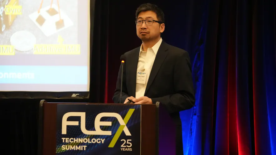
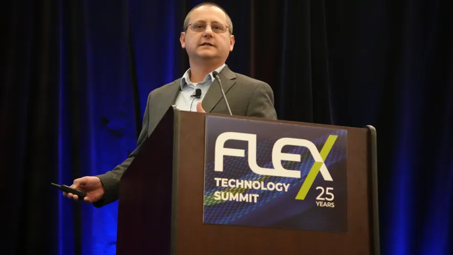
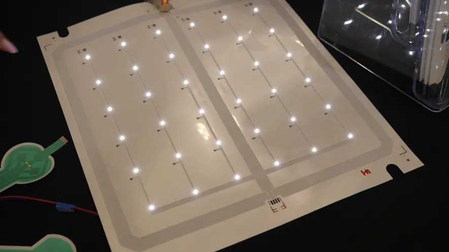
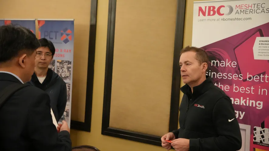
Highlights from Flex 2026
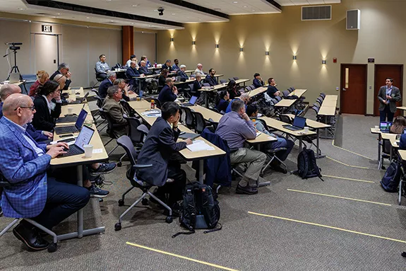
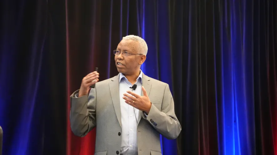
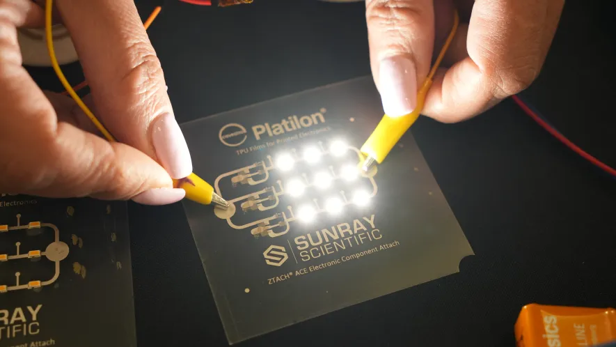
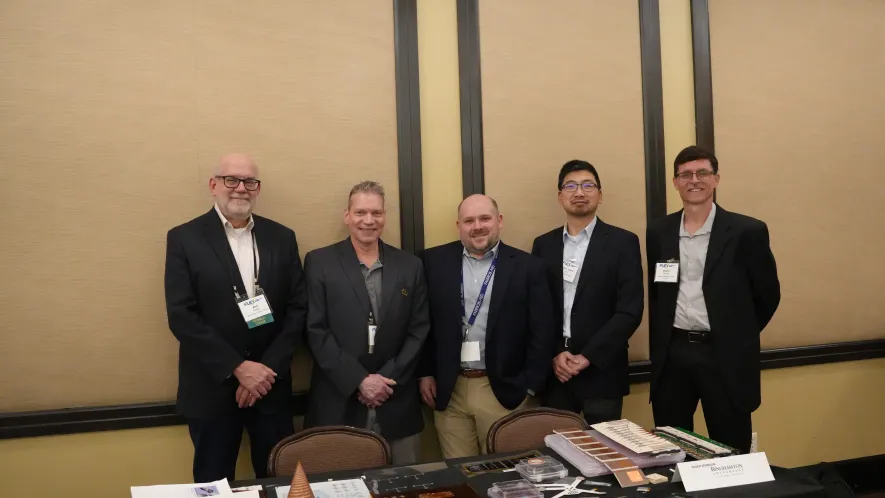
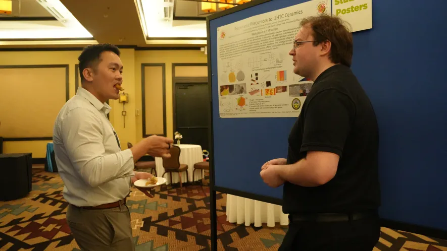
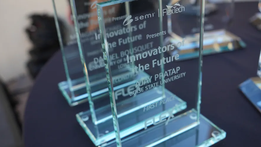
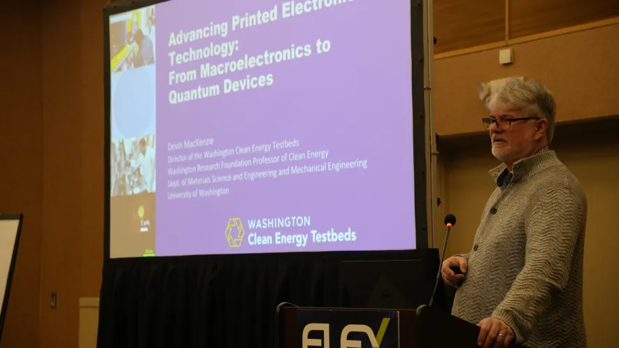
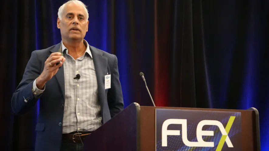
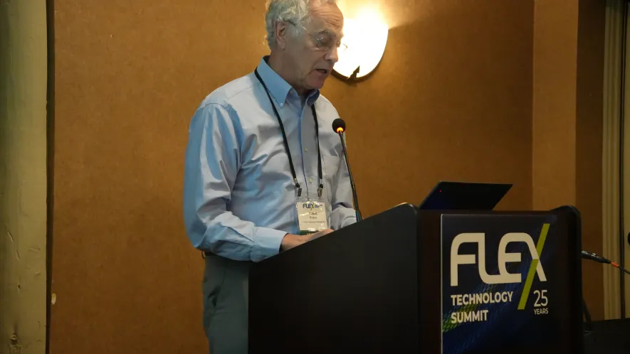
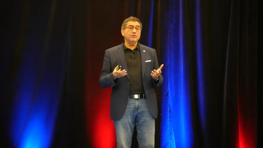
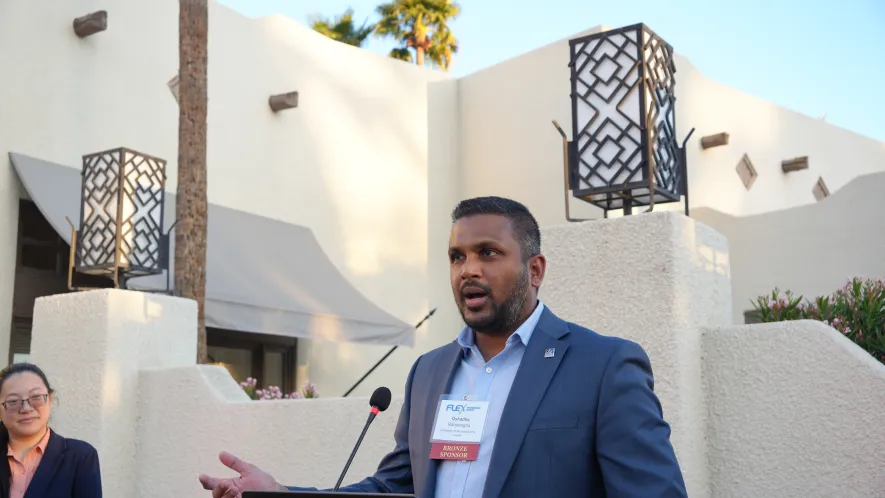
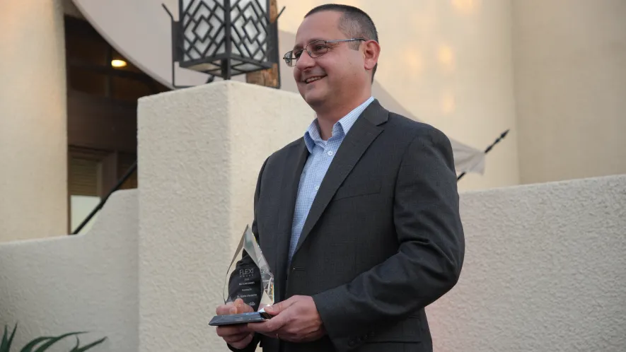
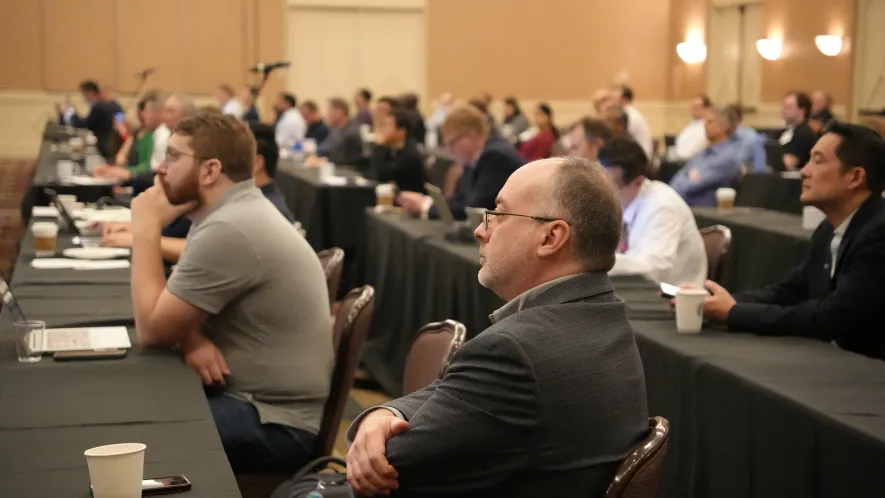
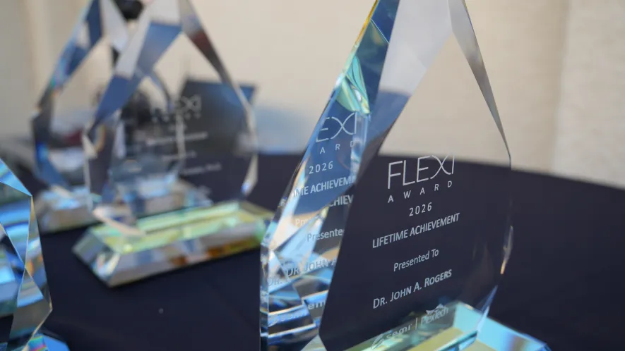
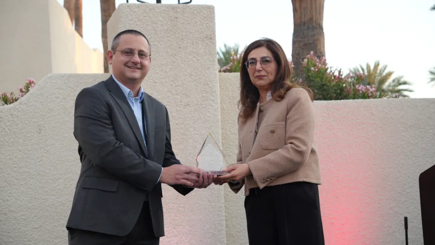
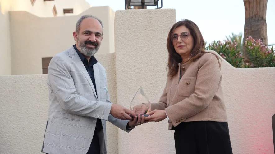
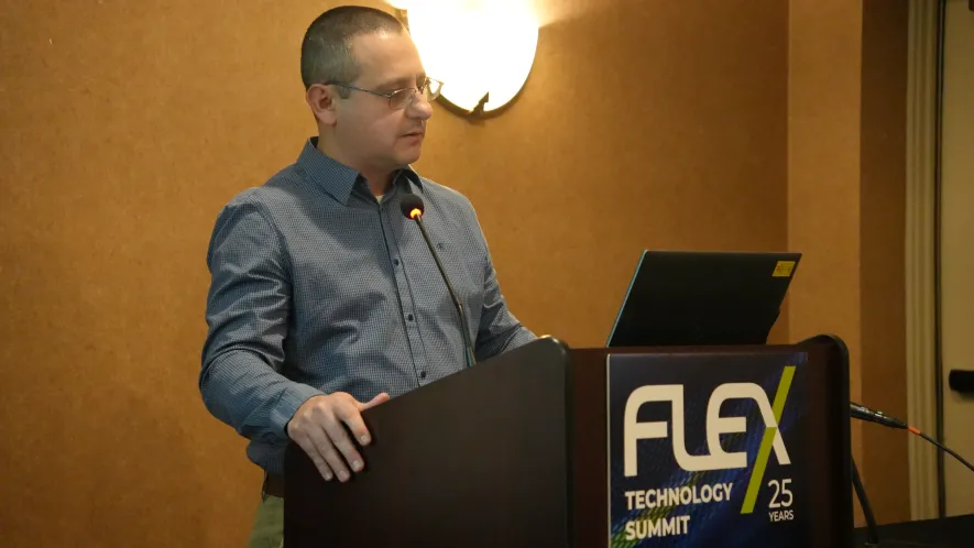
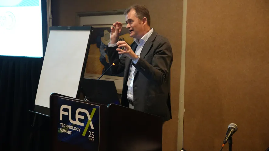
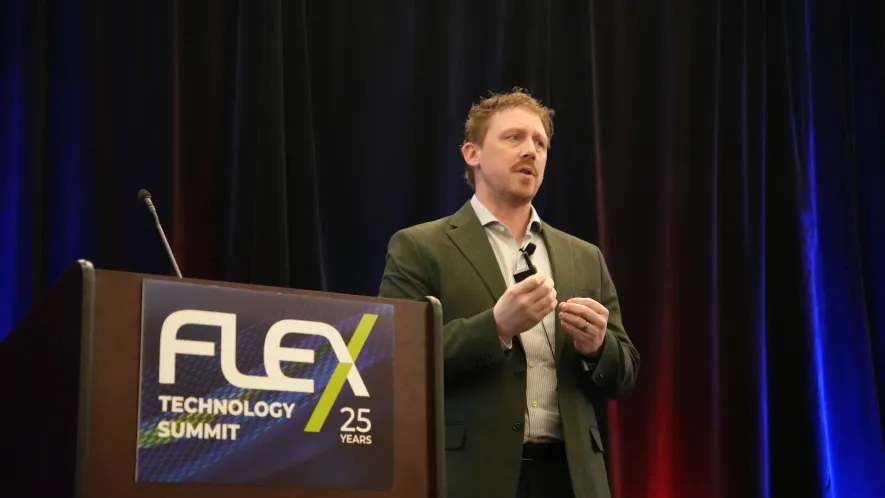
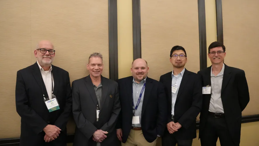
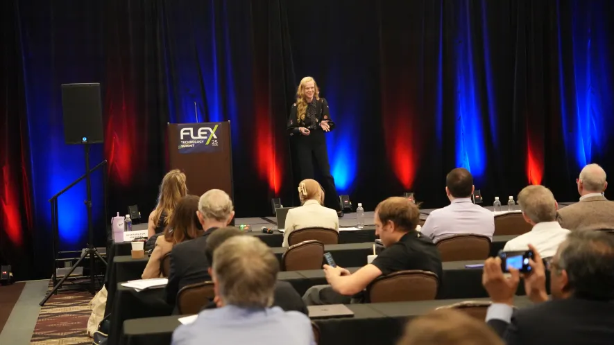
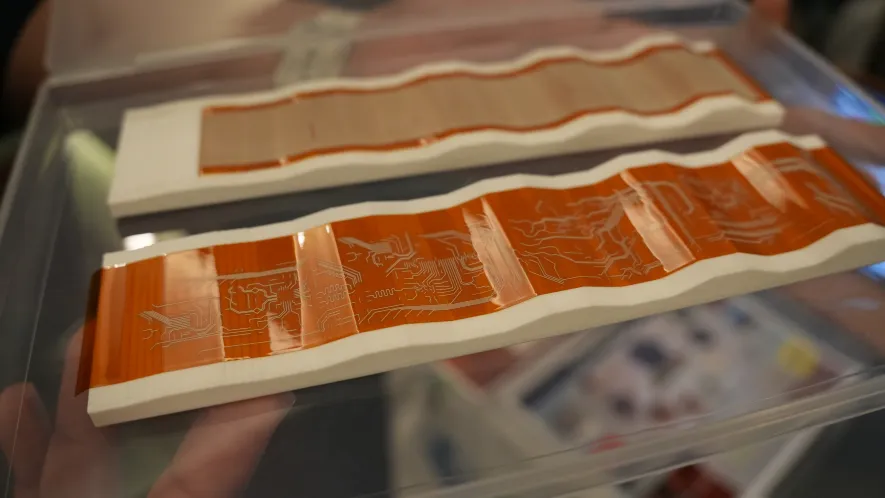
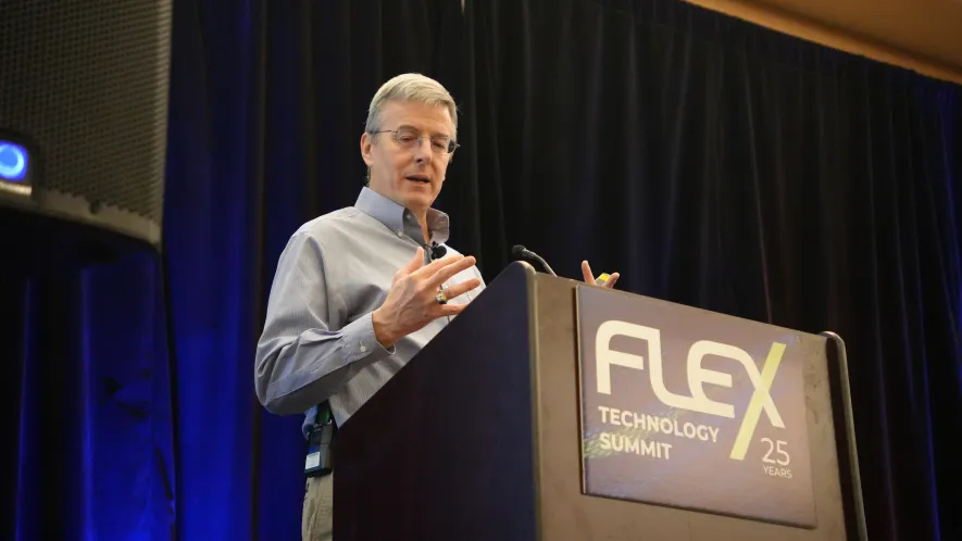
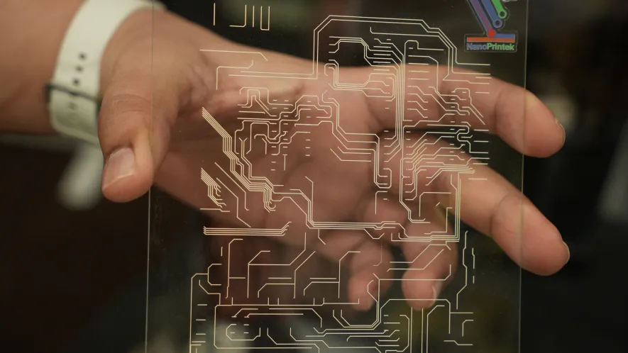
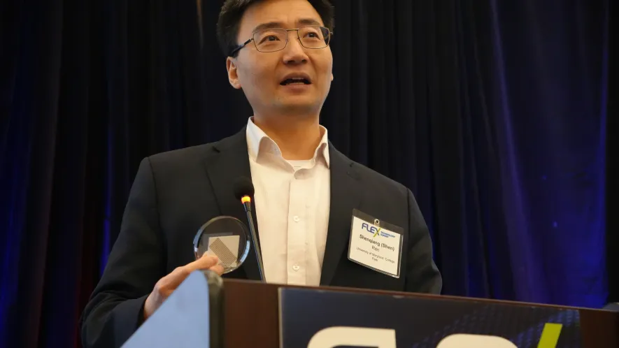
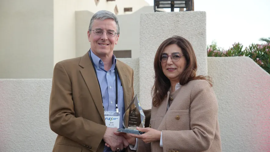
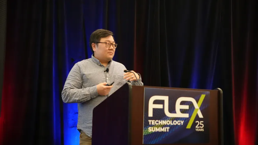
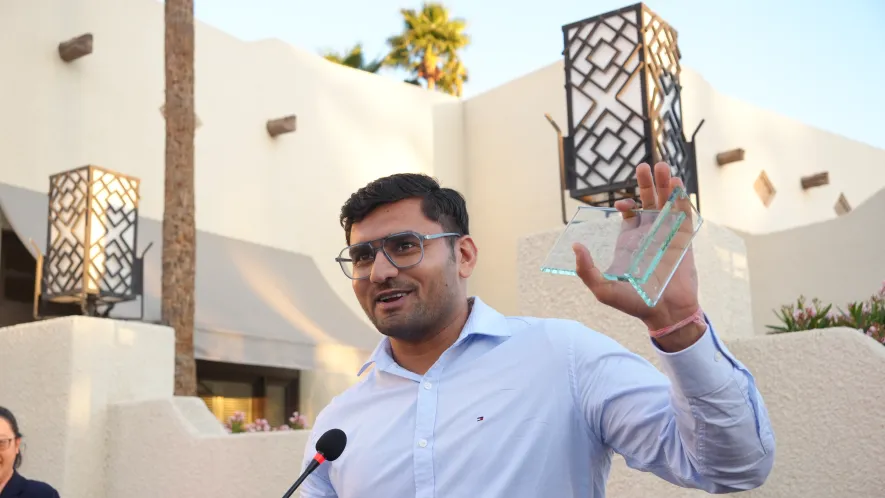
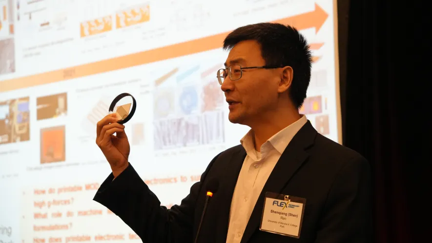
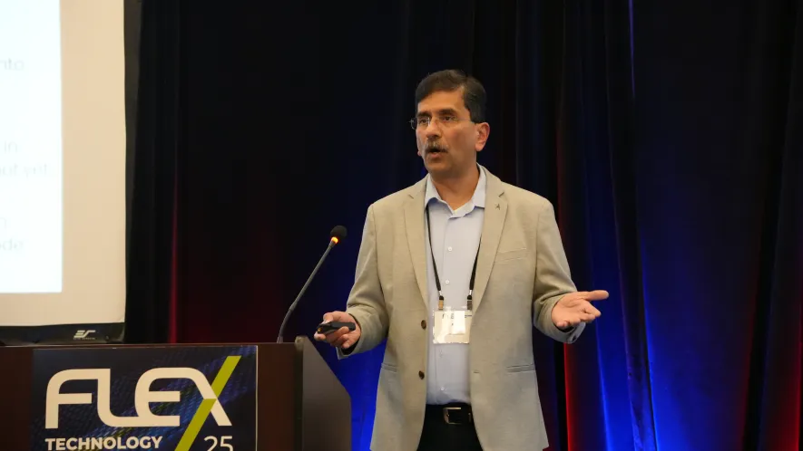
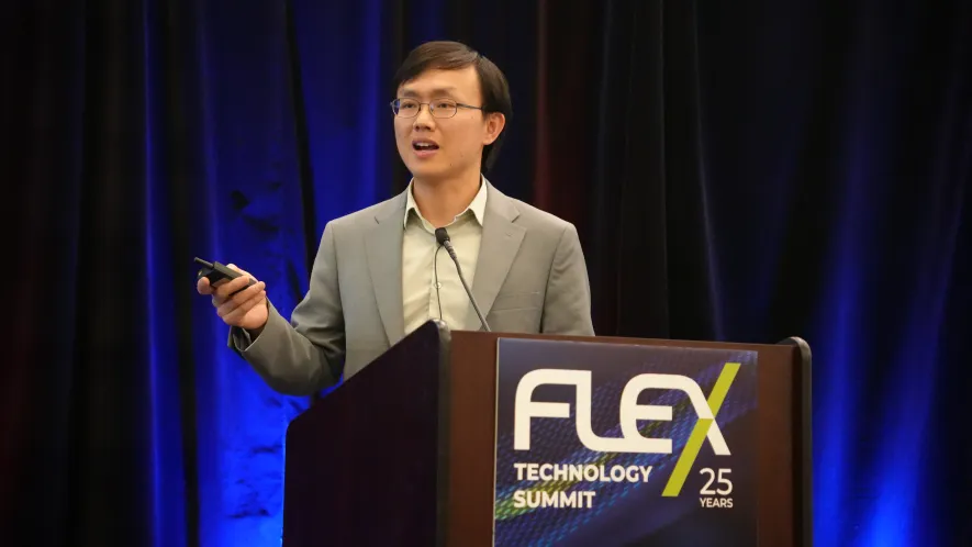
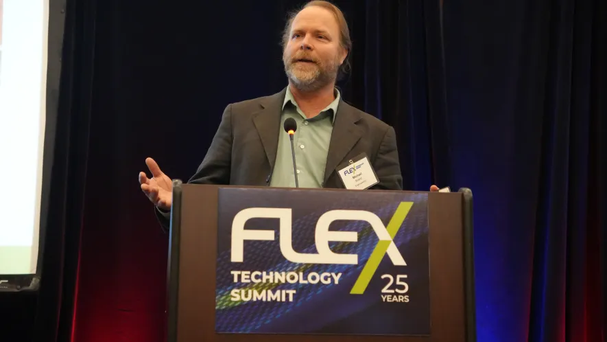
See some highlights from last year's FLEX Technology Summit. With a powerful speaker line-up, incredible networking, fascinating innovations, and amazing people.
NeoCity
194 NeoCity Way
Kissimmee, FL 34744
United States
Monday, April 21 (Medtronic Tour)
Medtronic Tour
(Tour sold out. Sign up for the waitlist.)
Join us for an exclusive one-hour tour of Medtronic’s facility, to explore its advanced operations in designing and manufacturing microelectronics for implantable medical devices.
Note: Space is limited to 24 participants.
Transportation will not be provided.
Tuesday, April 22 (Preliminary Agenda)
Registration and Breakfast
Vision and Mission of FlexTech
Printed Devices for High-Temperature Applications in Aerospace
Use of Gigahertz Ultrasound Imaging and Artificial Intelligence to Improve Printed Electronics
Soft Robots with Novel, High-Density Interconnects for Non-Destructive Inspection
Digital Twin in Nanofabrication Cleanroom
Break
Reliability Physics and Acceleration Factors for FHE Circuits under Sustained Temperature and Stresses of Daily Motion
Additively Manufactured Flexible Hybrid Capacitors and Antennas for Biosensing and RF Applications
Materials and Processes for High Volume Integration of Stretchable Circuits into E-Textiles
Printable Ink Materials and Electronics for Extreme Environments
Transparent Antennas - Product Market Fit & A Technology Update
Networking Lunch
FlexTech, What happening now?
Breakout Strategy Sessions
Attendees will break into groups for smaller discussions to identify challenges, prioritize those challenges and identify opportunities on critical issues discussed throughout the morning session.
Break
Breakout Sessions Readout
Student Poster Networking Reception & Mayo Clinic Lab for Function Tour
Mayo Clinic
IERB Building
5951 E. Mayo Blvd
Phoenix, AZ 85054
Mayo Lab Tour: If you're interested, please sign up at the registration desk. Space is limited to 20 participants and will be available on a first-come, first-served basis.
Note: Transportation to this reception will not be provided. (2 minute drive.)
Wednesday, April 23 (Preliminary Agenda)
Registration and Breakfast
Opening Remarks
Vision and Mission of NBMC
NBMC Gap Analysis Workshop AFRL Perspective
Graphene Field-Effect Transistors: Transforming Next-Generation Medical Diagnostics
Sweat Without Sweating: Exploring the Possibilities of Biochemical Monitoring with Passive Sweating
Bio-inspired Soft Electrodes for Robust and Reusable Bioelectronic Stickers
Break
Manufacturing of Low-Cost Wearable Physiological and Molecular Marker Monitoring Patches for DoD Applications
Fan-Out Wafer-Level Packaging for Flexible Medical Devices
Advancing Dermal Interstitial Fluid as a Viable Matrix for Accessible Diagnostics
Transdermal Optical Microneedle Sensors for Continuous Monitoring of Physiological Analytes in Interstitial Fluid
Shaping a Soft Future
Networking Lunch
NBMC, What's Happening Now?
Breakout Strategy Sessions
Attendees will break into groups for smaller discussions to identify challenges, prioritize those challenges and identify opportunities on critical issues discussed throughout the morning session.
Break
Breakout Sessions Readout
Networking Reception and Tours of Wexford Connect
Enjoy Networking, concurrent tours, and presentation content
850 Phoenix Bioscience Core
850 N 5th Street
Phoenix, AZ 85004
https://850pbc.com
5:00 pm - 5:30 pm: Tours of Wexford Connect (Limited to 30 people)
5:30 pm - 6:00 pm: Networking
6:00 pm - 6:15 pm: Welcome. Scarlett Spring, Executive Director, Phoenix Bioscience Core
6:15 pm - 7:00 pm: Panel Discussion:
Bridging Clinical Needs and Emerging Technology: Research, Implementation, and Scale.
Moderator: Chris Yoo, General Partner, Xcellerant Ventures
Panelists:
Suman Bose, Assistant Professor of Biomedical Engineering, Mayo Clinic
Hakan Ceylan, Assistant Professor and Principal Investigator, Mayo Clinic
Ross Bundy, CEO, CRISPRQC
Elsa Abruzzo, CEO, Anuncia Medical
Allen Waziri, CEO and Co-Founder, iCE Neurosystems
Note: Transportation will not be provided. (30+ minute drive.)
Thursday, April 24 (Preliminary Agenda)
Registration/Breakfast
Welcome Remarks
KEYNOTE: AI at the Point of Care: The Next Era of Intelligent, Patient-Centric Healthcare
Panel Discussion: The Arizona MDM2 Consortium - Investing in the Medical Technology Manufacturing Renaissance
Moderator: Chris Yoo, Founder and CEO and Regional Innovation Officer, MDM2 Consortium
Panelists:
Kiran Avancha, Chief Innovation Officer, HonorHealth
Rochelle Rivas, District Director for Healthcare Innovation, Maricopa Community Colleges
Alex Tessmer, Associate Director, BD Peripheral Intervention, Ideation
FIRESIDE CHAT: How can wearables and implantables improve care of the acutely ill patient?
Moderator: Jonathon Parker , Neurosurgeon, Director of Device-Based Neuroelectronics Lab, Mayo Clinic - Arizona
Participants:
Aman Verma, Hospitalist, Mayo Clinic, Arizona
Break
PANEL DISCUSSION: Health Data 2035: How do we Capture, Integrate, and Secure Health Data Streams From Wearables and Implantables to Improve Patient Care?
Moderator: Kiran Avancha, Chief Innovation Officer, Honor Health Innovations
Panelists:
Craig Norquist, Chief Innovation Officer, Honor Health
Matthew Anderson, Chief Medical Information Officer - Ambulatory, Honor Health
FIRESIDE CHAT: Stroke Care 2035- How Can Digital Health Data Transform Stroke Care?
Moderator: Jonathon Parker , Neurosurgeon, Director of Device-Based Neuroelectronics Lab, Mayo Clinic - Arizona
Participants:
Bart M. Demaerschalk, Vascular Neurologist, Mayo Clinic, Arizona
Chandan Krishna, Neuro-endovascular Neurosurgeon, Mayo Clinic, Arizona
FIRESIDE CHAT: Real-Time Oncology - How Can Wearables and Implantables Reshape Oncology Care in 2035?
Moderator: Jonathon Parker , Neurosurgeon, Director of Device-Based Neuroelectronics Lab, Mayo Clinic - Arizona
Participants:
Nandita Khera, Oncologist, Associate Chair of Digital Health, Mayo Clinic
Panel Discussion: The New Frontier of Long-Term Brain Monitoring: Brain Computer Interface Re-Imagined
Moderator: Randal Schulhauser, Founder and CEO, Schulhauser Associates LLC
Panelists:
Jonathon Parker, Neurosurgeon, Director of Device-Based Neuroelectronics Lab, Mayo Clinic
Allen Waziri, Neurosurgeon, Co-Founder iCE Neurosystems, iCE Neurosystems
Paul Gerrish, VP, Technology and Medtronic Fellow, Medtronic
Lunch
Opening Remarks
Enabling Personalized Healthcare and Wellness through the Integration of Electronics
Health on the Edge: AI, Wearables & The Future of Personalized Healthcare
Semiconductor Technologies for the Next Generation of Efficient and Innovative Medical Devices
Break
Panel Discussion: Digital Health Revolution: Insights and Innovations
Moderator: Douglas Kiehl, BioCrossroads/Purdue
Panelists:
Bharath Rajagopalan , Director – Strategic Marketing, Health & Wellness, STMicroelectronics
Anirban Bandyopadhyay, Senior Director, Global Foundries
Stephaney Shanks, Division Director, Integrative Health and Performance Sciences, BlueHalo
Deon Chen, Sr. Manager, HEOR Strategic Planning, BD
Evening Program Hosted by Venture Café
850 Phoenix Bioscience Core
850 N 5th Street
Phoenix, AZ 85004
https://venturecafephoenix.org/
Venture Café Phoenix is a dynamic weekly gathering where entrepreneurs, innovators, and business leaders connect to exchange ideas and build meaningful relationships.
Note: Transportation to this program will not be provided (30+minute drive)
Fireside Chat: Harnessing Semiconductor For transformational Advancements in HealthTech
Abstract
Moderator: Nandini Tandon
Panelists:
Jami Mei, VP of Business Development, Arizona Commerce Authority
Douglas E. Kiehl, Sr. Vice President, BioCrossroads
Mark Dydyk, Director of Engineering & Operations, Medtronic
Join us for a three-day workshop uniting SEMI Technology Coalitions: FlexTech, NBMC, and CAST
The workshop will delve into advancements, challenges, and gaps in critical technologies such as flexible hybrid electronics, hybrid electronics, and bio-signal sensing for real-time cognitive and physical state monitoring and augmentation and will feature AI for Metrology (AI4MT) sessions
8:00 am - 6:00 pm Off Add to Calendar 2027-02-16 08:00:00 2027-02-18 18:00:00 Flex Technology Workshop 2027 Join us for a three-day workshop uniting SEMI Technology Coalitions: FlexTech, NBMC, and CASTThe workshop will delve into advancements, challenges, and gaps in critical technologies such as flexible hybrid electronics, hybrid electronics, and bio-signal sensing for real-time cognitive and physical state monitoring and augmentation and will feature AI for Metrology (AI4MT) sessions NeoCity 194 NeoCity Way Kissimmee, FL 34744 United States SEMI.org [email protected] America/New_York public America/New_YorkRegistration
Registration for GES Taiwan 2026 is now closed.
If you have already registered, you will receive confirmation and onsite details by email ahead of the event. For questions about your registration, please contact David Chiang at [email protected].
Travel
Venue
GES Taiwan 2026 will be held at the Junior Ballroom, 5F, Taipei Marriott Hotel, in conjunction with SEMICON Taiwan 2026.
Hotel
Taipei Marriott Hotel
GES Taiwan 2026 takes place at the Taipei Marriott Hotel, Junior Ballroom, 5F, in conjunction with SEMICON Taiwan 2026. For questions about accommodation, please contact David Chiang at [email protected].
Introduction
The Global Executive Summit (GES) convenes senior leaders from across the semiconductor value chain to drive collective progress on the industry's most pressing energy and decarbonization challenges. Following the inaugural summit in Tokyo in 2025, GES returns in 2026 as the Executive Summit on Energy and Sustainability, held in Taipei, Taiwan.
Tokyo established four priority initiatives now under active delivery: Gas Substitution, Abatement, Clean Electricity, and Fab Upstream Materials. Taiwan moves that work from alignment to execution.
This is an invitation-only event.
Day at a Glance
The summit is structured around two sessions.
Morning Session (7:45 AM – 12:30 PM) + Lunch
Diamond Sponsor:

Face-to-face GES Executive Council (GESEC) meeting to review progress and challenges on GES 2025 calls-to-action driven initiatives and to also lay out 2027 direction. Attendance in this session is limited to current GESEC, Semiconductor Climate Consortium (SCC) and Energy Collaborative (EC) Leaders.
Afternoon Session (1:30 PM – 6:00 PM) + Happy Hour and Networking
Platinum Sponsors:
![]() | ![]() |
Gold Sponsors:
![]() |
This impactful session establishes the context for Taiwan's energy transition and semiconductor decarbonization. By pairing government keynotes and industry presentations with a public-private panel discussion, the session aims to surface key challenges and opportunities that can shape critical topics for inclusion in future GES Executive Council (GESEC), Semiconductor Climate Consortium (SCC) and/or Energy Collaborative (EC) initiatives.
Taipei Marriott Hotel,
Junior Ballroom, 5F (in conjunction with SEMICON Taiwan 2026)
Zhongshan District, Taipei City
Taiwan
Open to GESEC members, SCC and EC leaders, invited executives. By invitation. Not transferable.
Arrival and Registration
Executive Opening Remarks
Remarks
Setting the Stage and Introduction to Agenda
Keynote: Building the Business Case for Sustainability
Council Discussion: From Business Case to Action
Initiative Review: Gas Substitution
Initiative Review: Abatement
Networking Break
Initiative Review: Fab Upstream Materials
Initiative Review: Clean Electricity
Council Roundtable: 2027 Direction
Photo Call on Stage, Event Closing and Feedback Survey
All VIPs
Closing Comments
Networking Lunch
Open to GESEC members, SCC and EC leaders, and invited industry and government executives. By invitation.
Arrival and Registration
Welcome Attendees and Introduction to Agenda
Welcome Dignitaries and Official Opening of the GES
Group Photo, All VIP
Keynote: Energy Outlook
Keynote: GES, SCC & EC Addressing Emissions & Energy
Break
Keynote: Beyond Renewable Electricity — Next Strategic Resource for Semiconductors
Panel A: Opportunities for Public-Private Partnerships in Taiwan's Energy Transition (in Mandarin with simultaneous translation to English)
Keynote: Powering Sustainable Growth: Energy, Efficiency and Sustainability
Panel B: Taiwan's Energy Transition — Key Opportunities, Challenges and Calls to Action
Closing Remarks
Happy Hour and Networking
Contact
For inquiries, please contact David Chiang at [email protected].
Post-Show Report
San Francisco, CA
United States
Registration
※ Early-bird Registration Deadline: July 8 (Wed), 2026, 17:00 PM (KST)
| Early Bird | On-site | Group | |
| SEMI Member | KRW 308,000 | KRW 385,000 | KRW 275,000 |
| Non-Member | KRW 363,000 | KRW 330,000 |
※ Group registration fee applies to groups of five or more from the same company.
※ For group registration inquiries, please contact SEMI Korea Program Team at [email protected].
OVERVIEW
- Date: July 15(Wed), 2026
- Time: 08:30 - 17:00
- Venue: Convention Hall 1, 3F, Suwon Convention Center
- Language: Korean/English (Simultaneous interpretation will be provided)
- Organizer: SEMI Korea
SPONSORS
![]() | ![]() | ![]() |
![]() | ![]() | ![]() |
![]() |
NOTICE
- The agenda is subject to change at the discretion of the speakers.
- Presentation files agreed by speakers will be provided to attendees after the event through SEMI registration website.
CONTACT
- SEMI Korea Program Team ([email protected])
Convention Hall 1, 3F, Suwon Convention Center South Korea
South Korea
Welcome Reception
2026 Outlook for the Advanced Packaging Industry
Making 3DIC Manufacturable for AI: From Vertical Integration to Scalable Production
As AI systems push requirements for higher bandwidth, lower power, and increased integration density, 3D integrated circuits (3DIC) are moving rapidly from development to production. However, scaling 3DIC introduces complex application challenges across the manufacturing flow, where process interactions and control become critical.
This talk examines key 3DIC applications and process challenges, including high aspect ratio TSV etch, void free TSV fill, and dielectric deposition, required for reliable wafer and die level stacking. Emerging applications such as inter die gap fill for advanced chiplets integration and plasma dicing for improved yield, edge quality, and die strength further increase integration complexity and productivity demands.
The presentation highlights Lam Research innovations across etch, deposition and clean processes that enable tighter process windows, improved uniformity, and higher throughput. In addition, equipment intelligence and data driven control are increasingly essential to enhance yield learning and manufacturing productivity. Together, these advances are enabling scalable, high volume 3DIC manufacturing for next generation AI systems.
Advanced Packaging: Enabling AI at Scale
The future of compute will not be defined by silicon alone. As AI reshapes industries and economies, advanced packaging has become the foundation of the next era of innovation, enabling unprecedented gains in performance, efficiency, and scale. During his keynote, Yin Chang will explore how breakthroughs in heterogeneous integration, chiplets, and advanced manufacturing are transforming bold AI ambitions into deployable systems, and why AI leadership will depend not only on compute power, but on the ability to integrate and manufacture at scale.
Advanced Power Module Packaging Technologies
The rapid electrification of automotive and industrial systems is placing increasingly stringent demands on power semiconductor devices in terms of voltage capability, thermal performance, reliability, and system integration. This presentation reviews recent trends in power devices and power module packaging technologies aimed at improving performance while addressing cost and manufacturability constraints.
First, the fundamental differences between digital and power devices are outlined, followed by an overview of power device applications based on silicon (Si), silicon carbide (SiC), and gallium nitride (GaN) technologies, together with Amkor’s product portfolio.
Next, power module packaging technologies are discussed with a focus on key electrical and thermal challenges. Representative solutions, including advanced interconnects, cooling architectures, and embedded power modules, are introduced, along with a brief overview of Amkor’s technology roadmap.
Finally, the role of the Amkor Technology Japan R&D Center in supporting open innovation and global collaboration is briefly discussed.
Networking Break
Panel Discussion
Lunch
Advanced Packaging Technology for AI/HPC
The presentation explores advanced packaging technologies designed to meet the escalating performance and power efficiency demands of AI and High-Performance Computing (HPC). To overcome the limitations of traditional semiconductor architectures, System Technology Co-Optimization (STCO) is introduced as a critical framework for managing thermal crosstalk and enhancing heterogeneous integration. The discussion highlights key innovations, including Customized HBM (cHBM) for optimized base-die performance and Samsung's 2.xD packaging portfolio, which encompasses Cube S, Cube E, and Cube R. Specifically, the 2.3D Cube E leverages panel level packaging to enable larger interposers and increased HBM integration, significantly improving productivity and reducing silicon fab burdens. The technical achievements in PLP—such as precise warpage control and the realization of fine RDL patterns (2/2μm)—are detailed to demonstrate their viability for large-scale AI chips. Furthermore, the roadmap extends toward 3D integration and Co-Packaged Optics (CPO) to maximize bandwidth and energy efficiency. Finally, the importance of an ecosystem-wide collaboration is emphasized as the driver for future innovation in "More than Moore" technology. These advancements collectively provide a scalable path toward the next generation of AI hardware acceleration.
Latest Development Status of Glass Core Build-up Substrate
Glass core substrates exhibit low CTE and significantly higher rigidity than conventional organic substrates and are therefore regarded as promising core materials for next-generation build-up packages. However, a major challenge lies in the occurrence of SeWaRe defects (delamination in glass), which arise from thermal stresses induced by the mismatch in the coefficients of thermal expansion (CTE) between the glass material and the build-up resin.
To mitigate this issue, we proposed a structure in which the corner regions of each individual piece are formed from resin. However, considering the thermal history during chip mounting, it became evident that the suppression effect was insufficient. Therefore, an edge‑protection material was applied to relieve the stress concentrated at the edges of each individual piece. As a result, it was confirmed that SeWaRe defects could be effectively suppressed even under thermal loading.
Through these efforts, we successfully developed a glass core build-up package substrate incorporating 11 layers of single‑sided copper wiring (22 layers in total).
Beyond Moore's Law: How Silicon Photonics and Advanced Packaging Are Redefining HPC
AI and data-intensive workloads are outpacing what conventional semiconductor technology can deliver. Two innovations are stepping in to close the gap: Silicon Photonics, which brings optical-speed, low-power data transmission into the data center, and Advanced Packaging, which uses chiplets and 2.5D/3D integration to maximize performance and efficiency at the chip level.
This talk examines how these complementary technologies are reshaping HPC architecture—covering their current state, how they work in tandem, and the key technical and commercial barriers to large-scale adoption.
CPO Packaging: Challenges and Opportunities
Co-packaged optics (CPO) is emerging as a key enabler for scaling bandwidth while containing power and cost in next-generation AI and cloud infrastructure. By moving optical engines closer to the switch ASIC and shortening high-speed electrical reaches, CPO can reduce SerDes power, ease signal-integrity constraints, and increase overall front-panel bandwidth density. However, delivering these benefits at volume requires new approaches across package architecture, manufacturing, and system integration.
This presentation reviews the main packaging challenges that must be solved to industrialize CPO, including thermal management and heat spreading near high-power silicon, fiber attach and optical alignment tolerances, photonics/laser integration choices, high-density optical and electrical I/O, substrate and interposer selection, and reliability risks such as warpage, CTE mismatch, and contamination control. Test and rework strategy, yield learning, and supply-chain readiness (materials, assembly, and metrology) are highlighted as practical barriers to adoption.
The talk also outlines opportunities created by CPO packaging innovations—such as modular optical tiles, standardized fiber interfaces, advanced lid/heat-sink concepts, and co-design of electrical, mechanical, and optical domains—to unlock higher radix switches and lower system power. Attendees will leave with a structured view of technology tradeoffs, a roadmap of near-term versus long-term packaging options, and actionable considerations for bringing CPO from prototypes to deployable products.
Networking Break
Panel Discussion
Advanced Packaging Summit 2026, under the theme “Packaging the Future of AI – From Silicon to Photon,” will examine the evolution of packaging technologies in the AI era and their broader implications for the semiconductor industry. Featuring presentations by leading industry experts, the summit will explore market shifts driven by the growing demand for AI semiconductors, along with key technologies enabling advanced packaging. The program will also highlight the innovation journey from silicon-based integration technologies to photonics-based interconnects, which are essential to enhancing packaging productivity and scalability. Panel discussions in each session will further provide opportunities to exchange insights on real-world applications, technical challenges, and possibilities for cross-industry collaboration, while exploring new business opportunities and strategic perspectives created by advanced packaging technologies in the AI era.
8:30 am - 5:00 pm Off Add to Calendar 2026-07-15 08:30:00 2026-07-15 17:00:00 ADVANCED PACKAGING SUMMIT 2026 Advanced Packaging Summit 2026, under the theme “Packaging the Future of AI – From Silicon to Photon,” will examine the evolution of packaging technologies in the AI era and their broader implications for the semiconductor industry. Featuring presentations by leading industry experts, the summit will explore market shifts driven by the growing demand for AI semiconductors, along with key technologies enabling advanced packaging. The program will also highlight the innovation journey from silicon-based integration technologies to photonics-based interconnects, which are essential to enhancing packaging productivity and scalability. Panel discussions in each session will further provide opportunities to exchange insights on real-world applications, technical challenges, and possibilities for cross-industry collaboration, while exploring new business opportunities and strategic perspectives created by advanced packaging technologies in the AI era. Convention Hall 1, 3F, Suwon Convention Center South Korea South Korea SEMI.org [email protected] Asia/Seoul public Asia/SeoulSuggested Hotels:
Embassy Suites by Hilton Milpitas Silicon Valley
901 East Calaveras Boulevard
Milpitas, CA 95035
(408) 942-0400
Courtyard by Marriott Milpitas Silicon Valley
1480 Falcon Dr.
Milpitas, CA 95035
(408) 719-1966
Event Sponsors
Sponsorship Opportunities
Enhance your brand with our exclusive sponsorship packages. For details, contact:
Karim Somani
Email: [email protected]
SEMI HQ
673 S Milpitas Blvd.
Milpitas, CA 95035
United States
Morning, Day 1: August 5th, 2026
Emergent AI/ML Tools for Semiconductor Manufacturing Technology Optimization
Semiconductor manufacturing faces a broad set of complex challenges addressed through Yield Management Systems (YMS), Fault Detection and Classification (FDC), Run-to-Run (R2R) control, Design of Experiments (DOE), and Statistical Process Control (SPC). Existing machine learning approaches are predominantly scoped to individual process steps or short loops, leaving full-traveler analysis — essential for informed tool decisions such as hold, parameter adjustment, and recipe modification — largely unaddressed. Bespoke, step-specific models do not generalize across process nodes or design variants, and manually configuring analytical workflows for each new use case is time-intensive and error-prone as technology nodes diversify. General-purpose coding agents built on large language models (LLMs) partially close this gap by automating workflow generation, but they lack the semiconductor-specific domain knowledge required for robust, production-grade solutions: open-source ML packages carry no fab context, and proprietary data curation and signal-processing conventions are rarely captured in public training corpora.
This session shows how a fab-aware agentic approach closes that gap, focusing on three use cases: YMS, FDC, and Process DOE. It opens with a technical primer built on a common pipeline — preprocessing and feature reduction, uncertainty-aware imputation, regime-aware modeling (physics and virtual-metrology priors when data is scarce, data-driven as it grows), and interpretable attribution rather than black-box scores — instantiated differently across the three, with emphasis throughout on when a result can be trusted. YMS downselects high-dimensional metrology, imputes sparse measurements, and trains a tuned regressor ensemble (GPR, gradient-boosted trees, neural nets), with feature attribution (SHAP) mapped to process step and tool. FDC aligns traces, then layers univariate control limits (SPC) with multivariate anomaly detection (PCA, Hotelling T², MEWMA), per-sensor attribution, and alarm-budgeted limits that transfer across chambers. Process DOE designs experiments, fits uncertainty-aware surrogates (Gaussian processes), reduces dimensionality (PCA), and selects runs sequentially (single- and multi-objective Bayesian optimization). Attendees then see these techniques operationalized live by a domain-specific agentic platform and work directly with the agents on curated datasets.
By the end, attendees will understand how problem formulation, data characteristics, and method selection shape outcomes, and what distinguishes a domain-aware agentic workflow from a general-purpose coding agent. The session is interactive by design — participant choices steer the live analysis, and attendee input shapes how these capabilities evolve.
Real-Time Equipment Health Monitoring Using Gaussian Process Regression on Sensor Signals
Will present a real-time health monitoring method for semiconductor equipment using multi-sensor time-series signals. From a small set of baseline runs (typically 5–20), Gaussian Process Regression is used to learn expected sensor behavior and associated confidence bands over repeatable operating segments. At runtime, deviations from these bands are aggregated into health scores per sensor and segment to identify abnormal behavior early. The system automatically reports anomalies and raises warnings to support proactive maintenance and reduce unplanned downtime and quality risk. To address the O(N^3) training cost of standard GPR, we use a split-training approach that achieves linear scaling, keeping computation practical for production use.
Break
Predict Before Failure: A Predictive Maintenance Blueprint with NV-Tesseract and NeMoClaw
Semiconductor fabs generate high-volume, multivariate sensor telemetry from process tools, ambient monitoring systems, sub-fab equipment, etc. Scheduling maintenance operations depends on more than just reacting to alarms/alerts: teams need to forecast how equipment will behave and detect abnormal trajectories/baseline shifts before failures occur.
This session introduces an open Predictive Maintenance Blueprint that embeds NV-Tesseract as the core time series AI component. The pipeline performs multivariate forecasting on equipment sensor data, then runs diffusion-based anomaly detection on the forecasted window to flag emerging degradation patterns.
The blueprint is packaged as a reusable, deployable workflow with Hugging Face weight retrieval, configurable sensor channels, and structured outputs for downstream automation.
We extend this blueprint with NVIDIA NeMoClaw, treating predictive maintenance as an always-on agent workflow: an autonomous agent ingests sensor streams, invokes the NV-Tesseract pipeline, interprets anomaly scores, and produces operator-ready summaries and recommended actions under OpenShell runtime guardrails.
Together, this shows how foundational time series models and agent orchestration can be coupled to build a production-style Predictive Maintenance stack for semiconductor operations.
What the Audience Will Learn:
Predictive maintenance is shifting from threshold-based SCADA alarms to forecast-then-detect workflows that catch drift earlier on multivariate equipment signatures.
Foundational time series models (like NV-Tesseract) are increasingly deployed as components inside larger agent systems, not as standalone notebooks.
Semiconductor and industrial teams are adopting blueprint + agent patterns (similar to NeMoClaw deployments in EDA, simulation, and factory ops) to move from prototype to governed, repeatable workflows.
Practical lessons: multivariate sensor alignment matters; model weights and configs should be versioned and auto-retrieved; anomaly outputs must be explainable enough for maintenance engineers to trust and act on.
Architecture takeaways:
When to use multivariate forecasting vs. single-signal monitoring.
Why diffusion-based anomaly detection fits correlated, high-dimensional fab sensor data better than univariate reconstruction approaches.
How NeMoClaw can orchestrate the pipeline: data ingest → inference → thresholding → alert routing → human-in-the-loop review.
Lunch
Practical Agentic AI at Scale for Manufacturing: Lessons Learned from Large-Scale Deployments
Agentic AI is nearing mainstream adoption, yet many organizations still lack a clear strategy for deployments at scale. In order to bring LLM capabilities to manufacturing, companies need to go beyond what mainstream AI suppliers can deliver; they need AI deployments to be governed, reliable, repeatable, and scalable enough to earn trust and deliver measurable results. Most importantly, it must be grounded in and continuously integrate the knowledge of subject matter experts who understand the complexity of real systems and processes.
In this session, we will share lessons learned from deploying large-scale agentic AI solutions in the semiconductor industry. We will explore how SME expertise and operational context can be embedded into Agentic AI systems to create trusted, high-value results. Specifically, we will show how an auto-Triage/RCA a Facilities Anomaly event workflow can be set up such that, as the event triggers, an AI agents completes a first pass investigation that is ready for consumption by the end user shortly after an event triggers with an optional integration with CMMS systems to ease the creation of a work order to drive faster time to resolution and greater consistency in event disposition. We will also demonstrate how engineers can build custom apps and AI agents on demand, without requiring an AI specialist or extensive coding skills, while maintaining the structure and scalability needed for enterprise adoption. Attendees will leave with practical insights for enabling better, faster decisions across engineering, technician, and operator workflows.
Afternoon, Day 1: August 5th, 2026
Human-Machine Collaboration for Improving Semiconductor Process Development
One of the bottlenecks to building semiconductor chips is the increasing cost required to develop chemical plasma processes that form the transistors and memory storage cells1,2. These processes are still developed manually using highly trained engineers searching for a combination of tool parameters that produces an acceptable result on the silicon wafer3. The challenge for computer algorithms is the availability of limited experimental data owing to the high cost of acquisition, making it difficult to form a predictive model with accuracy to the atomic scale. Here we study Bayesian optimization algorithms to investigate how artificial intelligence (AI) might decrease the cost of developing complex semiconductor chip processes. In particular, we create a controlled virtual process game to systematically benchmark the performance of humans and computers for the design of a semiconductor fabrication process. We find that human engineers excel in the early stages of development, whereas the algorithms are far more cost-efficient near the tight tolerances of the target. Furthermore, we show that a strategy using both human designers with high expertise and algorithms in a human first–computer last strategy can reduce the cost-to-target by half compared with only human designers. Finally, we highlight cultural challenges in partnering humans with computers that need to be addressed when introducing artificial intelligence in developing semiconductor processes.
What the Audience will Learn:
How Bayesian optimization can help enhance speed-to-solution for semiconductor manufacturing.
Break
From Prediction to Action: Causal AI for Real-Time Root-Cause Analysis in Semiconductor Manufacturing
Semiconductor fabs generate massive volumes of data across tools, sensors, inspection systems, and process logs—yet most AI deployments remain predictive, identifying anomalies without explaining their root cause. This results in prolonged root cause analysis (RCA), costly downtime, and repeated trial-and-error fixes.
In this talk, we present a practical approach to moving from prediction to action using causal AI. By unifying multi-modal data like images, time-series signals, and process metadata into a single intelligence layer, we enable systems that reason about cause-and-effect relationships rather than correlations.
We will discuss how such systems can be trained efficiently using weak supervision and deployed at the edge to meet latency, privacy, and reliability requirements. We also highlight how continuous monitoring and model refinement in production ensure sustained performance in dynamic manufacturing environments.
Drawing from real-world deployments, we show how this approach reduces RCA time from hours to minutes, improves diagnostic accuracy, and enables prescriptive actions for faster yield recovery and improved operational efficiency.
What the Audience will Learn:
1. Why predictive AI falls short for RCA and how causal AI bridges the gap
2. How to build an “intelligence layer” on top of MES and traceability systems
3. Practical methods for leveraging limited labeled data
4. How to integrate multi-modal data (inspection images + sensor logs + process flows)
5. How to build AI agents that improve with more data
How this AI technique is being used in industry today (real deployments, lessons learned, impact): In semiconductor manufacturing environments, causal AI systems are being deployed alongside existing inspection and MES infrastructure to accelerate and improve root cause analysis.
In one deployment, defect patterns observed across multiple inspection stages were correlated with tool-level and process metadata. Instead of manual investigation across dozens of steps, the system identified a specific tool-stage interaction responsible for recurring defects. This reduced RCA time from 20–40 hours to under 10 minutes while improving diagnostic consistency.
Demo: Yes
Hands-on Session:
Yes, Applying weak supervision to label defect data with minimal manual effort
Interpreting causal relationships across process steps
Monitoring and updating models in a production-like setting
Reception
Morning, Day 2: August 6th, 2026
Get More from Your Sign-off Flow: Agentic AI That Makes Power & Signal Integrity Engineers Radically More Productive
Agentic AI is moving from research demos to production EDA flows, and the leverage is very clear in power and signal integrity sign-off, where engineers routinely write 1000+-API Python scripts, search for root causes through ~100 GB log files, and stitch results across half a dozen vendor tools. This talk presents our experiences with building, shipping, and supporting a multi-agent system for a production sign-off tool used on modern VLSI and 3DIC designs — covering what it took to move from a single LLM "wrapper" to a hardened agentic system that customers can actually trust with their IP.
We will walk through the full stack: a multi-agent architecture (code-generation, log-debug, RCA/diagnostics) built on a Deep-Agent framework; an Agent Skills pattern that makes diagnostic workflows modular, composable, and customer-extensible; MCP used in both directions (the Copilot consumes vector-DB and API knowledge as MCP, and the tool itself is exposed as an MCP server so other EDA agents and customer orchestrators can drive it); and a governance layer covering tiered action approval, API-hallucination guards, prompt sanitization, audit trails, and on-premise / air-gapped local-LLM deployment. We will close on the next frontier: cross-vendor agent-to-agent flows, for example, place-and-route → parasitic extraction → power integrity → timing — orchestrated through MCP, with humans setting policy at well-defined checkpoints rather than copy-pasting between tools.
The session is built for practitioners. A curated set of short demo videos recorded from real Agentic AI sessions on representative designs showing the agent generate scripts and run a multi-step RCA end-to-end, with explanations on what is happening under the hood at each step.
What the Audience Will Learn:
1. Reference architecture for a production EDA Copilot: Multi-agent decomposition (code-gen, log-debug, RCA), RAG over manuals/API catalogs, and tool execution inside the host EDA product.
2. The Agent Skills pattern for RCA / diagnostics: Composable Agent Skills (IR-drop RCA, anomaly detection, comparative run analysis) the orchestrator plans over and that customers can extend without touching the core.
3. MCP as a two-way integration framework: Consuming knowledge and tool capabilities as MCP and exposing the EDA tool itself as an MCP server so customer or partner agents can drive it.
4. Governance and guardrails for production: Tiered action approval, API-validation against the catalog to block hallucinations, prompt sanitization for IP, audit trails, and runaway controls.
5. A practical LLM strategy: Cloud frontier models, qualified open-weight local LLMs for air-gapped customers, and distillation + RL fine-tuning strategies with LLM-as-judge and production feedback.
6. The feedback flywheel: What to instrument to drive weekly prompt fixes, monthly workflow updates, and quarterly model improvements.
7. Cross-vendor agentic flows: Sequential chaining, parallel fan-out, and iterative loops across EDA tools over MCP.
How This AI Technique Is Being Used in Industry Today
The Copilot is a shipped, per-user binary that launches alongside a production sign-off tool, attaches to the user's interactive session, and runs entirely on customer infrastructure (cloud LLM or fully on-premise).
Demo Session: Curated Videos (20 min)
Rather than a live hands-on segment, the demo is a curated set of short, pre-recorded clips captured from real Copilot sessions on representative designs. This keeps the demonstration crisp and reproducible, and the speaker narrates each clip — calling out which agent, skill, or MCP call is firing and why.

Break
From Data Silos to Autonomous Discovery: Agentic AI in Semiconductors
Semiconductor manufacturing is increasingly challenged not by the availability of data, but by the difficulty of integrating and reasoning across fragmented, heterogeneous information sources spanning process data, metrology, and engineering knowledge. This session introduces a practical, system-level perspective on building agentic AI capabilities for semiconductor applications, beginning with foundational considerations in data definition, representation, and consistency across structured and unstructured domains.
The discussion focuses on how these foundations enable a transition from isolated analytics toward more integrated, decision-oriented systems. Architectural patterns are explored for combining data-driven models, simulation, and domain knowledge into cohesive workflows, with emphasis on reliable orchestration, traceability of reasoning, and appropriate human oversight—elements that are critical for deploying AI in high-stakes manufacturing environments.
The session concludes with an overview of how emerging approaches are extending these ideas toward more adaptive and semi-autonomous optimization systems. Attendees will gain a structured view of the end-to-end stack—from data preparation to decision support—and practical insights into considerations for adopting agentic AI methodologies in semiconductor manufacturing settings.
Building a Trustworthy Semiconductor Knowledge Base for Agentic Insight Generation
Semiconductor organizations face doubling advanced-node design costs, compressing design cycles, and scarce engineering talent while their most valuable asset, engineering knowledge, sits fragmented across schematics, waveforms, 8D reports, JIRA tickets, fab SOPs, and decades of tribal expertise. Generic search and AI tools routinely fail on this dense, technical content.
Drawing on real-world deployments at Broadcom, SanDisk, Altera, and Texas Instruments, Vectara will explore the solution architecture and real-world deployment of their domain-specialized Knowledge Hub and Agentic AI Platform designed specifically for the semiconductor lifecycle.
We'll walk through the multi-stage ingestion pipeline that preserves formulas, nested tables, and schematics natively; Vectara unified retrieval fabric that replaces fragmented, separately licensed point tools; and the agent layer that runs multi-hop, semantically deep queries across technical logs and historical failures - letting engineers surface root-cause indicators in plain language, no SQL required.
Crucially, the session will focus on what production-grade accuracy demands: grounded, citation-backed answers over complex IP for generating net-new insights, and streamline cross-team knowledge reuse that engineering teams, and agents can trust.
Lunch
Afternoon, Day 2: August 6th, 2026
Making Sense of Equipment Time‑Series Data: From Signals to Insight
Modern semiconductor equipment generates vast amounts of time-series and inspection data, but much of it remains under-utilized. This session presents a practical, end-to-end workflow—from data preparation and AI modeling (including anomaly, defect, and drift detection) to validation and deployment—using familiar manufacturing data. It also highlights how synthetic data and generative AI can accelerate model development while maintaining robust validation and engineering control.
What the Audience will Learn:
Attendees will learn how to turn equipment data into actionable insights using an end-to-end AI workflow—from data preparation to deployment. They will also see how multiple AI approaches, synthetic data, and generative AI can accelerate development while maintaining rigorous engineering validation.
Demo / Hands-on Session: Yes
Break
Achieving Business Results from Air-gapped Agentic AI Automation in Semiconductor Manufacturing - Lessons from the Field
Agentic AI has crossed a capability line where it can now effectively automate non-trivial portions of work that previously was only done by factory engineers - process engineers, yield engineers, test engineers, maintenance engineers. At Cohu, we have been working closely every week with our customers to roll out agentic capabilities that are leading to significant automation, yield, and capacity improvements. Along the way, we have needed to overcome significant constraints - such as prohibitions on providing sensitive process data to cloud AI providers - and had to manage the more complicated issue of integrating agentic AI into legacy systems and processes. In this talk I can share some of ways that our customers are benefiting from agentic AI and talk about some of the learnings gained through these various deployments.
What the Audience will Learn:
Key learnings for the audience a) real use cases of agentic AI in global semiconductor manufacturing companies; b) practical recommendations for how to prepare for and be successful with the deployment of agentic AI in semiconductor manufacturing.
Demo:
FDC model creation, and fault analytics
Yield analytics
Tester Operations Management
Test Engineering - lot disposition analytics
Maintenance optimization and predictive maintenance
Line support optimization
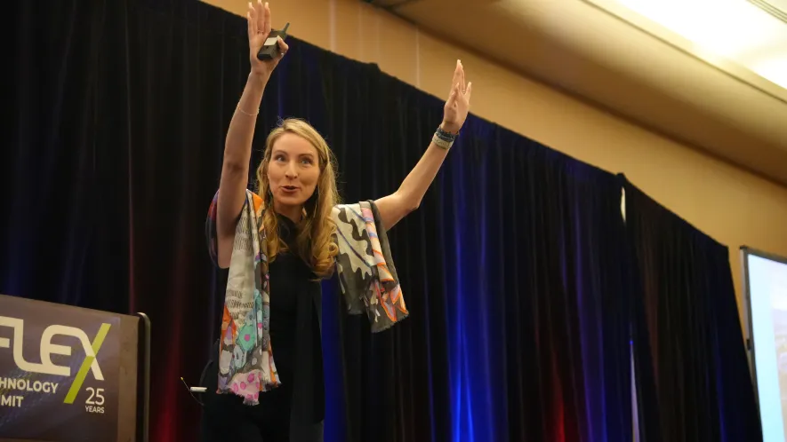
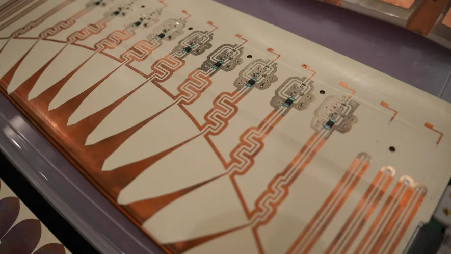
The SEMI Smart Manufacturing Initiative is hosting a two-day workshop titled "AI Techniques in Semiconductor Manufacturing" at SEMI HQ in Milpitas, CA, on August 5–6, 2026. This event is part of a continuing series focused on integrating advanced AI into the semiconductor landscape. The workshop is designed to help participants understand: The real-world deployment, impact, and lessons learned from AI techniques. Strategies for building observable and scalable multi-agent workflows. The industry transition from restrictive data silos toward autonomous discovery. Methods for achieving tangible business results and automation through diverse AI applications.
8:00 am - 5:00 pm Off Add to Calendar 2026-08-05 08:00:00 2026-08-06 17:00:00 AI Techniques in Semiconductor Manufacturing The SEMI Smart Manufacturing Initiative is hosting a two-day workshop titled "AI Techniques in Semiconductor Manufacturing" at SEMI HQ in Milpitas, CA, on August 5–6, 2026. This event is part of a continuing series focused on integrating advanced AI into the semiconductor landscape. The workshop is designed to help participants understand: The real-world deployment, impact, and lessons learned from AI techniques. Strategies for building observable and scalable multi-agent workflows. The industry transition from restrictive data silos toward autonomous discovery. Methods for achieving tangible business results and automation through diverse AI applications. SEMI HQ 673 S Milpitas Blvd. Milpitas, CA 95035 United States SEMI.org [email protected] America/Los_Angeles public America/Los_Angeles Register NowNangang District, Taipei City


Taiwan
Yashobhoomi
Delhi
India
Registration
Regular Pricing
$249 Members
$349 Non-Members
Cancellation Policy
Cancellations received on or before July 27, 2026, are fully refunded with a $50 processing fee. Refunds will not be issued for cancellations (including no-shows) made after July 27, 2026, and only substitutions are accepted with a written note from the registered attendee. Please email your cancellations or substitutions on company letterhead to [email protected].
Breaking Silos, Accelerating Innovation: Semiconductor & MedTech Converge Together
In a rare cross-industry gathering, MedTech pioneers and semiconductor innovators are coming together under one roof. The Semiconductor–MedTech Ecosystem Summit is designed to break down industry silos, connecting silicon innovators directly with medical device makers to accelerate the development of next-generation medical technology.
If you are building the future of medical devices, diagnostics, or connected care, this is where you secure your competitive advantage.
The Convergence: Three Focus Areas Driving the Next Frontier
By bringing these two massive industries together, we are accelerating the timeline for revolutionary healthcare. We will be diving deep into:
- Wearables & Continuous Care: Changing the game for personalized healthcare by enabling clinical-grade, untethered monitoring that moves with the patient.
- Advanced Medical Imaging: Pushing the boundaries of early detection through advanced imaging technologies that make the unseen visible.
- Edge AI & Predictive Health: The invisible engine underpinning rapid advancements in both MedTech and silicon. We’ll explore how processing at the edge allows for the pinpointing of diagnoses and treatments long before traditional symptoms appear.
SEMI Headquarters
673 S. Milpitas Boulevard
Milpitas, CA 95035
United States
Breakfast & Registration
Strategic Outlook
Welcome from GlobalFoundries
Keynote: No Chips, No Cure: Why Semiconductors Are the Invisible Infrastructure of Modern Healthcare
The Life Sciences Growth Engine Runs on Silicon
Networking
Break
Integration
Keynote: Exploring Enabling Approaches for Precision Medicine throughout the Drug Development Process
From Integration to Intervention: The Whole is Greater than the Sum of its Parts
Bioconvergence: How Semiconductor Innovation is Shaping the Future of Healthcare
Panel Discussion: The Role of Semiconductor in 5-10 Years in MedTech
Session Chair - Anirban Bandyopadhyay
Fritz Werder | Silicon Labs
Mohsen Askarinya | Medtronic
Girish Naganathan | Former Dexcom
Paru Deshpande | imec
Lea Drye | FDA
Networking
Lunch
Innovation
Keynote: "Health Sciences, Semiconductor & AI" A Transformational Confluence
Inference on the Edge: The Next Generation of Wearable Silicon for Healthtech
Microfabbed Silicon as a (Transformational) Pharmaceutical Material
Panel Discussion: Disruptive Innovation in MedTech for Therapeutic and Diagnosis
Session Chair - Melissa Grupen-Shemansky
Vibhu Sharma | Philips
Bharath Rajagopalan | STMicroelectronics
Laura Matz | Merck KGaA
Gregg Bartlett | GlobalFoundries
Networking
Break
Innovation
Semiconductor Innovations Enabling the Future of Healthcare
When Biology Becomes the Sensor: Semiconductor-Enabled Platform for Cellular Intelligence
Democratization of Ultrasonic Medical Imaging & Challenges
Beyond the Form Factor
Wrap Up
SEMI
Networking
Reception
Experience a one-of-a-kind convergence of silicon and clinical care. Connect directly with semiconductor foundries and MedTech OEMs on Aug 27 to accelerate next-gen medical devices.
8:00 am - 6:00 pm Off Add to Calendar 2026-08-27 08:00:00 2026-08-27 18:00:00 Semiconductor-MedTech Ecosystem Summit Experience a one-of-a-kind convergence of silicon and clinical care. Connect directly with semiconductor foundries and MedTech OEMs on Aug 27 to accelerate next-gen medical devices. SEMI Headquarters 673 S. Milpitas Boulevard Milpitas, CA 95035 United States SEMI.org [email protected] America/Los_Angeles public America/Los_AngelesRecommended Hotels
Embassy Suites by Hilton Milpitas Silicon Valley
901 East Calaveras Boulevard
Milpitas, CA 95035
(408) 942-0400
Courtyard by Marriott Milpitas Silicon Valley
1480 Falcon Dr.
Milpitas, CA 95035
(408) 719-1966
Registration
※ Early-bird Registration Deadline: May 7(Thu), 2026, 10: 00 AM (KST)
Registration Fee
- Early Bird
- SEMI Member: KRW 308,000
- Non-Member: KRW 363,000
- On site
- SEMI Member : KRW 385,000
- Non-Member: KRW 385,000
- Group
- SEMI Member : KRW 275,000
- Non-Member: KRW 330,000
※ Group registration fee applies to groups of five or more from the same company.
※ For group registration inquiries, please contact SEMI Korea Program Team at [email protected].
OVERVIEW
- Date: May 12(Tue), 2026 8:30-16:30 KST
- Venue: Convention Hall 2, 3F, Suwon Convention Center
- Language: Korean/English (Simultaneous interpretation will be provided)
NOTICE
- The agenda is subject to change at the discretion of the speakers.
- Presentation materials will be available for download after the conference via the SEMI Korea program registration website(https://semikrprogram.com), only for materials approved by the speakers for distribution.
- Parking fees are not provided.
SPONSORS
![]() | ![]() | ![]() | ![]() |
![]() | ![]() | ![]() | ![]() |
![]() | ![]() | ![]() | ![]() |
![]()
CONTACT
- SEMI Korea Program Team ([email protected])

Suwon Convention Center
South Korea
Welcome Reception
How Wafer Processing Is Reshaping the 3D Era for AI
AI is fueling unprecedented growth and accelerating demand for advanced devices. Its requirements for performance, power, and area scaling are driving memory and logic devices toward 3D architectures.
At the heart of this 3D transformation, processing steps must enable taller, perpendicular structures as well as smaller features. Meeting these requirements calls for new deposition and etch capabilities that did not exist before, leading to breakthroughs needed in areas such as atomic-level deposition and etch (ALD and ALE), high-aspect-ratio processing, dry resist EUV patterning, and the adoption of new materials like molybdenum (Mo). As a result, the transition to 3D devices will drive increased intensity of deposition and etch processing.
This presentation will explore how deposition and etch are critical to unlocking the future of 3D devices, with increasing velocity required to meet the demands of AI-driven innovation.
Integrated Materials Innovation in the AI Era
As the semiconductor industry navigates the challenges of dimensional and functional scaling in the artificial intelligence (AI) era, advanced materials science has emerged as a critical enabler for performance enhancement. Modern AI-centric architectures demand the integration of increasingly complex system-on-chip (SoC) designs with non-traditional material systems.
This work details a high-throughput methodology for the rapid down-selection and optimization of multi-element thin films, ensuring alignment with both physical and electrical key performance indicators (KPIs). Utilizing combinatorial physical vapor deposition (PVD) in conjunction with unit-cell electrical test vehicles, we systematically screen an expansive elemental compositional space to identify optimal candidates. Advanced machine learning (ML) algorithms are integrated into each phase of the development lifecycle—spanning precursor synthesis, process optimization, and heterogeneous integration—to satisfy the rigorous specifications of emerging device applications. The synergy between integrated materials engineering and AI-driven informatics significantly reduces the temporal gap between material discovery and device-level implementation.
AI for Scientific Discovery: EXAONE Discovery
Chemical and materials research faces increasing demands for data-driven automation and autonomous research systems due to vast exploration spaces and complex decision-making processes. In this talk, we introduce EXAONE Discovery as a Chemical Agentic AI system and present an integrated research framework designed to accelerate scientific discovery.
EXAONE Discovery is an agent-based system that tightly integrates property prediction, molecular generation, synthesis prediction, and literature/data extraction. Based on given research objectives, the system accumulates relevant data, generates candidate molecules using model-driven approaches, evaluates their properties, and derives feasible synthetic routes—automating the end-to-end discovery pipeline. Furthermore, it is designed to enable a closed-loop research paradigm by interfacing with autonomous laboratories, connecting design–prediction–synthesis–validation cycles. This allows hypotheses proposed by AI to be experimentally validated, with results continuously fed back into the system for iterative model improvement and optimization.
In this talk, we will demonstrate how this integrated approach enhances research productivity across various industrial use cases in materials discovery and optimization, and discuss future directions of Chemical Agentic AI.
Global Memory Technology & Market Outlook
Materials Challenges and Path Forward for Future Memory Scaling
Networking Break
Panel Discussion
Networking Lunch
Emerging Etching Chemistry for Advanced Semiconductor Manufacturing
The rising technical demands for advanced semiconductor device manufacturing, and the industry’s ambitious net-zero commitments necessitate the development of novel etch chemistries that deliver both technical excellence and environmental sustainability. This talk will present an overview of the emerging etching chemistries developed by Air Liquide for variety-targeted applications. These innovative chemistries focus on delivering improved performance with unique technical merits to address current industry challenges. Exemplified by a novel low Global Warming Potential (GWP) designed for general dielectric etch, its synergistic integration with advanced abatement solutions, and a simplified Life Cycle Analysis (LCA) - from raw material extraction through processing, manufacturing, distribution, and use, this presentation aims to provide insights into a pathway towards more sustainable semiconductor manufacturing processes.
Enabling Advanced Metallization with Selective Deposition
As device architectures scale toward the angstrom era, metallization has emerged as one of the most critical bottlenecks to continued improvements in power and performance. Shrinking feature dimensions increase resistance, heighten reliability risks, and add complexity in interconnects and contacts. At these scales, traditional approaches which uniformly affect all wafer surfaces are increasingly ineffective. They rely heavily on lithography to define placement, and struggle to address tighter geometries and growing sensitivity to interfaces. Selective deposition is a solution which enables atomicscale control of where metals grow, placing material only where it is needed, without relying on patterning. It also enables monocrystalline metal growth, eliminating grain boundaries to minimize contact resistance.
This presentation will highlight how Applied Materials’ integrated materials solutions are enabling multiple inflections through area selective metallization. Selective Cobalt Capping technology encapsulates copper interconnects, improving adhesion, suppressing electromigration, and extending copper reliability to advanced nodes. Applied’s Selective Barrier eliminates a highly resistive interface at the interface of interconnect wiring. For contact fill, Applied developed Selective Tungsten (W) as a liner-less gap-fill solution that eliminates traditional liner/barrier layers and enables bottomup, seamfree metal fill. Finally, we introduce Selective Molybdenum (Mo) deposition that carries lowresistivity contact scaling forward as dimensions approach the fundamental scaling limits of W. Applied’s state-of-the-art atomic layer deposition tool for molybdenum delivers bottom-up, single-crystal Mo growth, enabling the next generation of contact scaling.
Next Generation Cleaning Processes and Materials
Cleaning processes originally relied on wet etch based patterning. However, dry etching now performs the majority of the patterning work, so wet etching is no longer needed for most pattern creation steps. Consequently, the focus of cleaning has shifted from patterning to the removal of contaminants. To obtain a clean surface, we must eliminate unwanted contaminants without any side effects such as pattern damage, collapse, material loss, or corrosion.
However, in the current era of 3 D structured devices such as V NAND, GAA, and 3 D DRAM, lateral wet etching is essential for patterning 3 D devices, and the proportion of wet etching in cleaning processes is increasing. Additionally, different kinds of selectivity such as concentration selectivity and area selectivity, have become important, in addition to conventional material selectivity. Sometimes we have to remove a film uniformly even though there are seams and voids. In addition, pattern loading has become a critical factor in lateral removal processes. We must solve these loading issues to achieve better performance and yield.
From time to time we must use more flexible, multi step processes; therefore, premixed chemistry is not enough to meet our purpose. Due to the flexibility of dry (gas phase) cleaning, the portion of dry cleaning has been increasing sharply. Area selectivity has also become another challenge. We must etch without corner rounding or climbing, and we want to perform anisotropic etching.
Conversely, based on the generic clean roadmap, high aspect ratio cleaning and low consumption cleaning will remain continuous challenges. Super critical CO2 drying is a solution for pattern collapse in HAR patterns, yet a dryer that is milder than CO2 but better than conventional IPA dryer technology is still required. In terms of chemical reduction, the puddle process may be a solution, but some side effects related to temperature consistency and cleanliness differences due to fluid dynamics must be resolved before implementation.
Networking Break
Panel Discussion
Adjourn
AI Enabled Materials Breakthroughs: From Molecules to Manufacturing
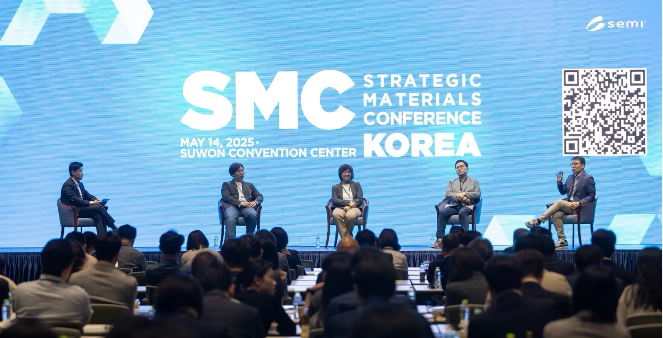
The transition toward an AI-driven technological landscape is redefining the paradigm of materials innovation across the semiconductor industry. In response, SMC (Strategic Materials Conference) Korea will spotlight next-generation semiconductor materials and process innovation strategies that enable and accelerate AI-driven advancements.
This conference brings together leading companies representing the global semiconductor ecosystem to share strategic directions and practical insights into materials innovation, from material design to real-world manufacturing processes.
The first session will focus on materials strategies for the AI era, exploring market and technology trends as well as AI-driven development approaches to provide a comprehensive view of next-generation semiconductor innovation. The second session will offer an in-depth exploration of process-ready materials essential for advanced semiconductor manufacturing, highlighting practical applications in areas such as photoresists, etching chemistry, and cleaning processes.
By convening key players across the semiconductor ecosystem, this conference provides a unique platform to gain a holistic perspective on the present and future of materials innovation in the AI era. Participants will have the opportunity to gain valuable technical insights while fostering collaboration and connections across the industry.
8:30 am - 4:30 pm Off Add to Calendar 2026-05-12 08:30:00 2026-05-12 16:30:00 SMC (Strategic Materials Conference) Korea 2026 AI Enabled Materials Breakthroughs: From Molecules to ManufacturingThe transition toward an AI-driven technological landscape is redefining the paradigm of materials innovation across the semiconductor industry. In response, SMC (Strategic Materials Conference) Korea will spotlight next-generation semiconductor materials and process innovation strategies that enable and accelerate AI-driven advancements. This conference brings together leading companies representing the global semiconductor ecosystem to share strategic directions and practical insights into materials innovation, from material design to real-world manufacturing processes. The first session will focus on materials strategies for the AI era, exploring market and technology trends as well as AI-driven development approaches to provide a comprehensive view of next-generation semiconductor innovation. The second session will offer an in-depth exploration of process-ready materials essential for advanced semiconductor manufacturing, highlighting practical applications in areas such as photoresists, etching chemistry, and cleaning processes. By convening key players across the semiconductor ecosystem, this conference provides a unique platform to gain a holistic perspective on the present and future of materials innovation in the AI era. Participants will have the opportunity to gain valuable technical insights while fostering collaboration and connections across the industry. Suwon Convention Center South Korea SEMI.org [email protected] Asia/Seoul public Asia/Seoul