downloadGroupGroupnoun_press release_995423_000000 copyGroupnoun_Feed_96767_000000Group 19noun_pictures_1817522_000000Member company iconResource item iconStore item iconGroup 19Group 19noun_Photo_2085192_000000 Copynoun_presentation_2096081_000000Group 19Group Copy 7noun_webinar_692730_000000Path
Skip to main content
Default Banner Image

In Person

Registration

Conference Pricing

Member: $1,555

Non-Member: $1,865

Krish Raghunath
Program Manager, Programs & Committees, SEMI
[email protected]

+
United States ESGS Event Tile Executive Technical

Travel

ESGS Hyatt Regency Phoenix

Hyatt Regency Phoenix—Book your room!  

122 North Second Street, Phoenix, Arizona, 85004

Service and Benefits 
  • $219/night
  • No resort fee
  • Standard high-speed wireless Internet access
  • Shuttle Transportation (Phoenix Premium Outlets, Aji Spa & Whirlwind Golf Club) 


ESGS Hyatt Regency Phoenix

Thank You to Our ESGS 2026 Sponsors

Platinum

Entegris

Gold

Pall Corporation 170x65
Thermo Fisher Logo 170x65

Silver

Bronze

Event

Diversified CPC International Logo 170x65

Become a Sponsor

View the 2026 ESGS Sponsorship Brochure

Sponsoring will associate your company with the industry's most respected senior executives. Sponsorship opportunities can be tailored to meet your specific branding and marketing objectives.

Contact Tim Janes at +1.720.939.4992 or [email protected]

Exhibitor Floorplan | View the Companies You Will Meet


The Electronic Specialty Gases & Systems Conference (ESGS) provides a forum of engagement and learning around the market, technology trends, and market drivers for electronic gases. The conference includes sections focusing on developments in the bulk, rare and specialty gas markets that are critical to the continued growth of the electronics industry.

The conference is designed for executives, buyers, product managers, and strategic planners from the electronic gases value chain including end-users, producers, and equipment suppliers. The conference features knowledgeable experts in the industry, who understand the key developments and challenges unique to this market.

Hyatt Regency Phoenix
122 N 2nd St
Phoenix, AZ 85004
United States

TUESDAY, NOVEMBER 10, 2026

7:00 am - 8:00 am

Breakfast

8:00 am - 8:05 am
Mike Corbett
Mike Corbett
Managing Partner
Linx Consulting

Opening Day Remarks

8:05 am - 8:45 am

Opening Keynote

8:45 am - 9:15 am
Bruce Gall, Google
Bruce Gall
Strategic Partnerships
Google

Breaking the Commercial Deadlock: Industry-Led Strategies for Low-GWP Adoption

9:15 am - 9:45 am

U.S. Semiconductor Public Policy Update

9:45 am - 10:15 am
Berc Kalanyan
Research Chemical Engineer
NIST

Measuring the Future: CHIPS Metrology Program Updates

10:15 am - 11:00 am

Networking Break

11:00 am - 11:30 am
Gustavo Albuquerque, Intel
Gustavo Albuquerque
PTD Gas Systems Engineer
Intel

Gas Systems Challenges as Moore’s Law Advances
11:30 am - 12:00 pm
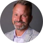
Mark O'Neill, Entegris
Mark O'Neill
Vice President, R&D and Engineering,
Entegris

12:00 pm - 1:15 pm

Lunch

Vapor Phase Materials and Electronics Specialty Gases

1:15 pm - 1:20 pm
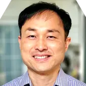
Venkat Pallam
Venkat Pallam
Deputy CTO & Technology Director, Thin Film Processing
Air Liquide

Opening Session Remarks

1:20 pm - 1:50 pm
David Mandia_LAM
David Mandia, PhD
Staff Process Engineer
Lam Research

Large Grain Molybdenum Deposition

1:50 pm - 2:20 pm
Feng Li, Air Liquide Advanced Materials
Feng Li
Senior R&D Manager
Air Liquide Advanced Materials

Solid Precursor Delivery: Challenges and Solutions

2:20 pm - 2:50 pm
Rachel Potter EMD
Rachel Potter
VP, Specialty Gases
EMD Electronics

Tungsten Powder Supply Chain Issues & Impacts

2:50 pm - 3:35 pm

Networking Break

Contamination Control and Yield
3:35 pm - 3:40 pm
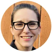
Sarah Vogt
Sarah Vogt
Director, E/R&D Gas Purification
Entegris

Opening Session Remarks

3:40 pm - 4:10 pm
Vindhya Kunduru
Vindhya Kunduru
Supply Chain Engineer
Intel

IRDS YE WECC Gas Team Update 2026

Latif Ahmed, Intel
Latif Ahmed
Senior Microcontamination Engineer
Intel
4:10 pm - 4:40 pm
Rocky Gipson, Entegris
Rocky Gibson, PhD
Senior Research & Development Manager
Entegris

Defining and Solving Contamination Challenges of Hydrogen Halides
4:40 pm - 5:10 pm
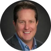
Steve Bovair, Isowater Corporation
Steve Bovair
Sales Manager
Isowater Corporation

Deuterium Supply Chain & Purity Considerations

5:10 pm - 5:20 pm
Mike Corbett
Mike Corbett
Managing Partner
Linx Consulting

Closing Remarks

WEDNESDAY, NOVEMBER 11, 2026

7:00 am - 8:00 am

Breakfast

New Technology Advancements

8:30 am - 8:40 am
Mike Corbett
Mike Corbett
Managing Partner
Linx Consulting

Opening Day Remarks

8:40 am - 8:45 am
Ashwini Sinha
Linde

Opening Session Remarks

8:45 am - 9:15 am
Heejeong Kim, Samsung
Heejeong Kim
Staff Engineer
Samsung Electronics

Isotropic Dry-Cleaning Technology for Next-Generation Semiconductor Devices

9:15 am - 9:45 am
Natalie Grancharov Camacho
Vice President Business Development, Electronics
ASP Isotopes

Zero-Nuclear-Spin Isotopes: Bridging Electronic Gases, Semiconductor Fabs & Quantum Computing

9:45 am - 10:15 am
Elizaveta Kossoy
Elizaveta Kossoy
Principal Scientist
EMD Electronics

Tailoring New Etch Gases to Challenging Applications

10:15 am - 11:00 am

Break

11:00 am - 11:30 am
Calvin Chen, Qnity
Calvin Chen
Senior Engineer
Qnity Electronics

Sealing in Advanced Semiconductor Gas Delivery: Permeation, Contamination, and Reliability Tradeoffs

11:30 am - 12:00 pm
Jake Armstrong, Micron
Jake Armstrong
Principal Chemical Engineer
Micron

AI Applications in Automated Gas Handling/Cylinder Changeout

Jonathan Graham
Johnathen Graham
Senior Sales Engineer
Wonik Holdings USA
12:00 pm - 12:30 pm
Kris Chupka, Nippon Sanso Matheson
Kris Chupka
Director of R&D, Gas Analysis
Nippon Sanso Matheson

Point of Use NANOCHEM Purifiers for Ultra-High Purity Inert Purge Gas Delivery in EUV Lithography Tools

Facilities and Infrastructure

12:00 pm - 1:30 pm

Lunch

1:30 pm - 1:35 pm
Kurtis Fairley
Kurtis Fairley
Director, Technical Programs North America
Edwards Vacuum

Opening Session Remarks

1:35 pm - 2:05 pm
Kassey Rydberg, NY CREATES
Kassey Rydberg
Director of Environmental, Health, and Safety
NY Creates

Advancing Sustainable Semiconductor Innovation: NY Creates' High NA EUV Lithography Center
2:05 pm - 2:35 pm
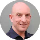
Ilya Zabelinsky, ISRL
Ilya Zabelinsky
CTO
ISRL

Industry Collaboration, Roadmaps, and Pre-Competitive Action in Sub Fab
2:35 pm - 3:05 pm
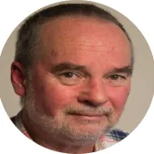
Kim Fjeldsted
Kim Fjeldsted
Sr. Applications Specialist
Ceres Technologies

Precursor Sources to Process Chamber: Principles of Delivery and Control

3:05 pm - 3:50 pm

Break

Sustainability

3:50 pm - 3:55 pm
Peilun Sun headshot
Peilun Sun
Consortium Manager, SCC
SEMI

Opening Session Remarks

4:25 pm - 4:55 pm
Chris Jones
Chris Jones
Environment and Sustainability Manager
Edwards Vacuum

Abatement Update / Catalytic

4:55 pm - 5:25 pm
Blake Ericson, Onterris
Blake Ericson
Business Manager
Onterris

Bridging the Measurement Gap: Enhancing Sustainability Compliance via Emissions Monitoring

5:25 pm - 5:30 pm
Mike Corbett
Mike Corbett
Managing Partner
Linx Consulting

Closing Remarks

6:00 pm - 8:00 pm

Networking & Poster Session Reception

THURSDAY, NOVEMBER 12, 2026

7:00 am - 8:00 am

Breakfast

Gas Metrology

8:00 am - 8:10 am
Nithin Yathapu
Nithin Yathapu
Senior Director, Yield Strategy
Intel

Opening Session Remarks

8:10 am - 8:40 am
Berc Kalanyan
Research Chemical Engineer
NIST

Stability of MoCl5 in Heated Canisters and During Delivery

8:40 am - 9:10 am
Chad Nelson
Product Manager
Process Insights

Fast Impurity Measurements in Electronic-Grade Rare Gases
9:10 am - 9:40 am
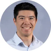
Tony Kou, Thermo Fisher Scientific
Tony Kou
Senior Applications Specialist
Thermo Fisher Scientific

Real-Time PPT Impurity Detection in Ultra-High Purity Gases for Semiconductor Fabs

9:40 am - 9:50 am
Mike Corbett
Mike Corbett
Managing Partner
Linx Consulting

Closing Remarks

Market Review and Updates

10:20 am - 10:30 am
Mark Thirsk
Mark Thirsk
Managing Partner
Linx Consulting

Opening Session Remarks

10:30 am - 11:00 am
Duncan Meldrum, Headshot
Duncan Meldrum
Chief Economist and Founder
Hilltop Economics

Does the Global Economy Matter for Semiconductors?

11:00 am - 11:30 am
 Inna Skvortsova
Inna Skvortsova
Research Manager, Market Intelligence
SEMI

SEMI Fab Capacity and Equipment Update
11:30 am - 12:00 pm
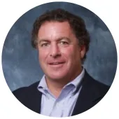
Phil Kornbluth
Phil Kornbluth
Founder & President
Kornbluth Helium Consulting

Helium Market Overview, Outlook & Trends
12:00 pm - 12:30 pm
Andy Tuan, Linx Consulting
Andy Tuan
Managing Director, Asia
Linx Consulting

Specialty Gas Market Update

- SEMI U

Driving Innovation Across the Electronic Gases Ecosystem

ESGS 2026 will take place at a new venue—the Hyatt Regency Phoenix—from November 10–12, building on the overwhelming success and momentum of last year’s event.

Off Add to Calendar 2026-11-10 00:00:00 2026-11-12 00:00:00 ESGS 2026—Electronic Specialty Gases & Systems Conference Driving Innovation Across the Electronic Gases EcosystemESGS 2026 will take place at a new venue—the Hyatt Regency Phoenix—from November 10–12, building on the overwhelming success and momentum of last year’s event. Hyatt Regency Phoenix 122 N 2nd St Phoenix, AZ 85004 United States SEMI.org [email protected] America/Phoenix public America/Phoenix 1

Share on LinkedIn

Let your LinkedIn connections know you’re attending ESGS! 

Spread the word and share our social media content with your connections so that they can join you there, too.

SEMI U Course

Monday, November 9, 2025 | 8:00am-5:00pm

Enhance your ESGS Conference experience with this exclusive SEMI U training course led by Jean-Pierre (JP) Deluca, a leak detection expert with more than 40 years of experience across the semiconductor, aerospace, automotive, medical, pharmaceutical, and refrigeration industries.

Fundamentals of Vacuum Technology and Helium Leak Detection is a comprehensive course designed to provide attendees with a practical understanding of vacuum systems, leak formation, leak measurement, and helium leak detection techniques used in semiconductor, aerospace, research, manufacturing, and high-technology industries. Participants will learn the principles of vacuum generation, gas flow, outgassing, permeation, conductance, pumping technologies, and helium mass spectrometer leak detection. The course also covers leak rate determination, industry standards, troubleshooting techniques, and real-world leak detection applications to help improve equipment reliability, product quality, and process performance.

What Attendees Will Learn

Upon completion of this course, attendees will be able to:

  • Define leaks, leak flow, virtual leaks, and their impact on vacuum systems and product quality.
  • Understand contaminant sizes, equivalent leak hole sizes, and leak-related defects.
  • Explain vacuum fundamentals, including pressure measurement, gas density, vacuum scales, and temperature effects.
  • Identify sources of gas loads, outgassing, permeation, and virtual leaks, and apply methods to minimize their impact.
  • Understand vacuum flow regimes, conductance, and how they influence pumping performance.
  • Compare rough vacuum and high-vacuum pumping technologies, including rotary vane, scroll, Roots, and turbomolecular pumps.
  • Understand the operation and capabilities of helium mass spectrometer leak detectors.
  • Explain helium properties, sources, applications, and why helium is the preferred tracer gas for leak testing.
  • Select and apply appropriate helium leak testing methods, including sniffing, accumulation, hard vacuum, bombing, and split-flow techniques.
  • Interpret leak detector response times, background helium levels, and published leak detector specifications.
  • Establish leak rate acceptance criteria and understand common leak rate units and conversions.
  • Troubleshoot high helium background conditions and improve leak detection sensitivity.
  • Apply leak detection principles to real-world vacuum systems and large vacuum chamber testing applications.
Who Should Attend

This course is intended for:

  • Semiconductor equipment engineers and technicians
  • Vacuum system engineers and maintenance personnel
  • Manufacturing, process, and reliability engineers
  • Field service engineers and installation specialists
  • Quality, test, and validation engineers
  • Research and development personnel
  • Aerospace and defense manufacturing personnel
  • Leak detection and vacuum equipment users
  • Facilities and equipment support personnel
  • Individuals new to vacuum technology or helium leak detection who require a practical, industry-focused foundation

Recommended Experience: No prior leak detection experience is required. A basic understanding of manufacturing, engineering, or technical equipment operation is helpful but not necessary.

Already attending the ESGS Conference? Add this SEMI U course to your registration for just $695 and gain valuable technical knowledge from one of the industry's most experienced instructors.

Interested in the course only? You can register for the SEMI U Course Only Pass for $795, making this training accessible even if you are not attending the full ESGS Conference.


Register Now
Event format
Tab Order
Overview
Agenda
New Tab 2
Registration
Travel
Sponsors
New Tab 1
Promote in calendar
On

REGISTRATION

Registration
  • Early-Bird Registration Deadline: Wed, July 9, 5PM (KST)
  • Group Registration Deadline: Fri, July 4, 5PM (KST)
  • Registration fee includes a boxed lunch provided at the venue.  


[Group]

  • SEMI Member : KRW 275,000
  • Non Member: KRW 330,000
    * Group registration fee applies to groups of five or more from the same company.
    * For group registration inquiries, please contact SEMI Korea Program Team([email protected]).

[Early Bird]

  • SEMI Member: KRW 308,000
  • Non Member: KRW 363,000

[On site]

  • SEMI Member: KRW 385,000
  • Non Member: KRW 385,000
Registration
South Korea APS2025_banner Business Technical

OVERVIEW

  • Date: July 16(Wed), 2025
  • Time: 09:00 - 17:00
  • Venue: Convention Hall 2, 3F, Suwon Convention Center
  • Language: Korean (Simultaneous interpretation will NOT be provided.)
  • Organizer: SEMI Korea  


SPONSORS


NOTICE

  • The agenda is subject to change at the discretion of the speakers.
  • Presentation files agreed by speakers will be provided to attendees after the event through SEMI registration website.


CONTACT

  • SEMI Korea Program Team ([email protected])
  • Simultaneous interpretation will NOT be provided.

Convention Hall 2, 3F, Suwon Convention Center
South Korea

9:00 am - 9:30 am
Choon Lee
Choon Lee
Intel

System Level Advanced Packaging

Rapidly evolving progress of AI and HPC has significantly increased computational and memory needs such as higher performance, lower power consumption, and wider memory bandwidth with reduced latency. An end application of AI/HPC comes down to Datacenter construction. Meeting the challenge of delivering this processing power in the datacenter requires systematic innovation from the device to the datacenter level. It starts with integrating highly optimized, domain-specific accelerators which should be integrated into advanced 2.5D and 3.5D packaging that minimize losses and power for high-speed communication while taking advantage of workload power management. AI computing introduces significant challenges for energy consumption and thermal management. Power delivery network is crucial for CPU, GPU and NPU power and performance of which solution can be DTC, IVR, mtal-insulator-metal (MIM) capacitor and thin film inductor, backside power rail, etc..  While Moore’s law has continued to yield transistor scaling necessary for these applications, the ever growing demand from models for AI training and inference pushes Si scaling in conjunction with the advent of advanced interconnects via disaggregation and reaggregation of chips in advanced packaging.  
We will discuss with examples and the challenges of utilizing packaging elements to their full potential and discuss how co-optimization is crucial to achieving the best results for any given set of system requirements and constraints.  

※Biography

9:30 am - 10:00 am
TaeKyeong Hwangv
TaeKyeong Hwang
Amkor Technology Korea

Advanced Packages for AI/HPC

10:00 am - 10:30 am
신상훈
SangHoon Shin
Assistant Professor,
Hanyang University

Advanced Packaging and Reliability: Technologies Shaping the Next Generation

Advanced semiconductor packaging is now central to enabling continued performance scaling as conventional transistor scaling slows. This seminar introduces cutting-edge trends in advanced packaging, including 2.5D and 3D integration, fan-out wafer-level packaging, chiplet-based architectures, and glass interposers for optical I/O in AI and HPC systems. These technologies offer enhanced performance, form factor reduction, and system-level integration capabilities critical for future computing platforms.
Leveraging prior industry experience, this talk highlights real-world applications and challenges in designing and qualifying advanced SoC packages. Examples include CoWoS-based AI chip packaging, hybrid bonding techniques, and thermal design optimization for high-power systems.
As packaging structures become increasingly complex, reliability emerges as a critical bottleneck. The seminar explores major failure mechanisms such as thermal-mechanical fatigue, electromigration, interfacial delamination, and Through Glass Via (TGV) degradation. Reliability analysis methods including FEA-based stress modeling, time-to-failure prediction, and advanced failure diagnostics will be introduced.
By combining packaging innovation with reliability engineering, the talk aims to provide a comprehensive perspective on the technological and practical issues that must be addressed to enable robust, high-performance semiconductor systems in the AI and data-driven era.

※ 연사정보

10:30 am - 11:00 am
Sang Hyun Han
Sang Hyun Han
NOVA

Pushing the Boundaries: Challenges and Opportunities in Panel-Level Packaging Technology

As the AI era progresses, semiconductor devices are increasingly adopting 3D architectures to boost performance and power efficiency. At the same time, system technology co-optimization (STCO) is advancing through the use of chiplets and advanced wafer-level packaging. As the industry integrates more chips into chiplets, the size of interposers continues to grow. However, wafer-level packaging faces limitations in accommodating large interposers due to the constraints of 300mm wafer shapes and temporary carriers.
This trend is driving a shift toward panel-level packaging (PLP) to support higher packaging unit counts. Despite its potential, PLP still faces significant challenges—particularly in terms of process development and process control.
This paper explores the technical trends in panel-level packaging, focusing on the current challenges and potential solutions related to process control.

※ Biography

11:00 am - 11:20 am

Break

11:20 am - 12:30 pm
All speakers

Panel Discussion

1:30 pm - 2:00 pm
Jinho_An
Jinho An
Senior Director/ Technologist,
Applied Materials

Presentation New Innovations Enabling Fine Pitch D2W Hybrid Bonding

Heterogenous integration and advanced packaging is behind the technology that is enabling today’s AI and high-performance computing. This is done through complex architecture that utilizes platforms including microbumps, through silicon vias (TSV), high density fanout and hybrid bonding (HB). The integration of chiplets using any combination of these technologies is allowing the industry to extend the Moore’s law and overcome limitations of the Von Neumann architecture. Hybrid bonding is an especially appealing technology that helps improve power and performance (higher I/O density), as well as thermal management. Sub-10 ㎛pitch die-to-wafer (D2W) HB is already in production1) for 3DIC and the industry working on HB technology for High Bandwidth Memory as well2). However, there are continuous challenges for D2W that require new innovation in both processing and metrology & inspection (M&I), and also unique challenges for both logic and memory applications specific to its integration. The presentation will discuss how logic and memory HB technologies are different and what process and M&I technologies are needed to facilitate HVM of the HB technology across different applications. Process challenges including low temperature bonding, die warpage management and dicing will be discussed, while M&I challenges include the transition to e-beam technology for HB enablement.

1) R. Agarwal et al., “3D Packaging for Heterogeneous Integration”, IEEE ECTC, July 2022
2) Lee et al., “A Study on D2W Cu Bonding Technology for HBM Multi-die Stacking”, IEEE ECTC, May 2024

※Biography

2:00 pm - 2:30 pm
Taehong Min
Taehong Min
Samsung Electro-mechanics

Trend and Technology of Glass Package Substrate

2:30 pm - 3:00 pm
이동환
Dong Hwan Lee
Samsung SDI

Design and Development of High Thermal Conductive Molding Compounds for Advanced Packaging Applications

The ongoing miniaturization and increased integration density in electronic circuit systems, particularly in advanced technologies such as DRAMs for Through-Silicon Via (TSV) and High Bandwidth Memory (HBM), have elevated thermal management to a critical challenge in microelectronic packaging. The functional performance, operational lifespan, and reliability of electronic devices fundamentally depend on efficient thermal dissipation. As power densities escalate, enhancing the thermal conductivity of EMCs has become imperative for effective heat removal from increasingly complex electronic components. Consequently, research efforts focused on developing epoxy resins with superior thermal conductivity and identifying appropriate high-conductivity fillers represent the most viable approaches to addressing thermal management challenges in contemporary microelectronic systems.
Recently, we have successfully developed a high-performance epoxy molding compound (EMC) that solves critical thermal management challenges in advanced microelectronic packaging applications. Not only do these compounds provide extremely safe protection of integrated circuits from moisture, mobile ion contaminants and adverse environmental conditions, including temperature fluctuations, humidity and mechanical stress, but the enhanced thermal and mechanical properties of EMC formulations address the heat dissipation requirements of advanced technologies such as small electronic circuit systems, especially TSV and HBM applications.

3:00 pm - 3:30 pm
Prof. Yunhyeok Im
Prof. Yunhyeok Im
Georgia Institute of Technology

Next-Generation Thermal Strategies: The Liquid Cooling Revolution for AI Chips

3:30 pm - 3:50 pm

Break

3:50 pm - 5:00 pm
All Speakers

Panel Discussion

Next-generation semiconductor packaging technologies are advancing rapidly in response to the explosive growth of high-performance semiconductor markets, including AI chips and HBM. At the Advanced Packaging Summit 2025, industry leaders from top global companies will share the latest developments and insights in advanced packaging technologies. The morning session will spotlight core technologies such as SLP and PLP, while the afternoon session will feature in-depth presentations on essential next-generation packaging technologies including hybrid bonding, glass substrates, materials for heat control, and liquid cooling solutions. Each session will also include panel discussions to encourage broad and practical exchanges of technical experiences, offering valuable opportunities for networking. We invite you to explore the future direction of next-generation semiconductor packaging with global industry experts and expand both your insights and business horizons at this premier event.

9:00 am - 5:30 pm Off Add to Calendar 2025-07-16 09:00:00 2025-07-16 17:30:00 Advanced Packaging Summit 2025 Next-generation semiconductor packaging technologies are advancing rapidly in response to the explosive growth of high-performance semiconductor markets, including AI chips and HBM. At the Advanced Packaging Summit 2025, industry leaders from top global companies will share the latest developments and insights in advanced packaging technologies. The morning session will spotlight core technologies such as SLP and PLP, while the afternoon session will feature in-depth presentations on essential next-generation packaging technologies including hybrid bonding, glass substrates, materials for heat control, and liquid cooling solutions. Each session will also include panel discussions to encourage broad and practical exchanges of technical experiences, offering valuable opportunities for networking. We invite you to explore the future direction of next-generation semiconductor packaging with global industry experts and expand both your insights and business horizons at this premier event. Convention Hall 2, 3F, Suwon Convention Center South Korea SEMI.org [email protected] Asia/Seoul public Asia/Seoul
Event format
Promote in calendar
Off
United States Image Training

Don't miss this chance to grow your knowledge, build your network, and accelerate your journey in the semiconductor industry.  


Course Options: 

PFAS Compounds in Semiconductor Environment: Half Day Course

  • Per- and Polyfluoroalkyl substances (PFAS) are a group of over 15,000 compounds which have been used in a variety of different industries due to their unique properties. Over the past two decades, their presence in water and the human body has become of increasing concern, with studies linking certain PFAS to adverse effects in the organisms studied. This has led to increasing consumer awareness, litigation, and the regulation of PFAS compounds. This course provides an in-depth review of PFAS compounds, their history, market drivers, regulations, current uses in the semiconductor industry, and methods for sampling and analysis, over the entire semiconductor value chain.

Semiconductor Device Manufacturing in a Cleanroom (Best Practices to Improve Product Reliability and Yield)

  • This course is designed for people who utilize cleanrooms. Semiconductor device manufacturing is a complex process that involves working in a cleanroom with a wide range of specialized equipment and materials. Many challenges must be overcome to meet production goals. This course provides the fundamentals and thought processes to improve your production reliability and yield. This course is intended for mechanical engineers, process engineers, test engineers, quality assurance engineers, and technicians.

Overview of Semiconductor Manufacturing

  • This course offers a solid foundation in semiconductor manufacturing, from basic concepts to advanced techniques, providing practical insights into the tools, processes, and technologies driving the industry.

Phoenix Convention Center
100 N 3rd St
Phoenix, AZ 85004
United States

SEMI U

Finish your show experience with SEMI U training sessions! 

Learn from experienced industry leaders across a wide range of topics. Choose a course that aligns with your goals and gain valuable insights to advance your role in the dynamic world of semiconductors.

Following the overwhelming success of last year’s inaugural trainings—where 125+ industry professionals, both seasoned and new, participated in five pre-show sessions—we’re expanding! This year, we’re offering three sessions the last day of the show to meet the growing training demand as the industry’s talent gap continues to widen. 


8:00 am - 4:00 pm Off Add to Calendar 2025-10-09 08:00:00 2025-10-09 16:00:00 Trainings at SEMICON West Finish your show experience with SEMI U training sessions! Learn from experienced industry leaders across a wide range of topics. Choose a course that aligns with your goals and gain valuable insights to advance your role in the dynamic world of semiconductors.Following the overwhelming success of last year’s inaugural trainings—where 125+ industry professionals, both seasoned and new, participated in five pre-show sessions—we’re expanding! This year, we’re offering three sessions the last day of the show to meet the growing training demand as the industry’s talent gap continues to widen.   Phoenix Convention Center 100 N 3rd St Phoenix, AZ 85004 United States SEMI.org [email protected] America/Phoenix public America/Phoenix Register Now
Event format
Promote in calendar
Off
United States Image Training

Don't miss this chance to grow your knowledge, build your network, and accelerate your journey in the semiconductor industry.  


Course Options: 

Advanced Packaging (Chiplets, WLP, Flip Chip, 3D Stacking)

  • This 1-day course addresses IC packaging, assembly, and package/substrate interconnections. It stresses the impact of the IC and end product requirements, i.e., “smaller, better, cheaper” their influence on the manufacturing processes. Topics include area packaging- ball grid arrays, flip chip, fanout, stacking die and chip scale packages, and the assembly technologies – chip & wire, tape automated bonding, and flip chip, as is emerging technologies namely, 3-D and stacked die, and packaging reliability issues.

Basic Electronics & Troubleshooting

  • This course provides students with a fundamental understanding of electronics and troubleshooting techniques. Topics covered include current, voltage, resistors, capacitors, inductors, diodes, and transistor fundamentals. Students will learn to differentiate between AC and DC power, understand digital and analog circuits, and interpret electronic component datasheets.  The course offers a comprehensive overview of the theory, operation, and applications of essential testing equipment, including the Volt-Ohm-Meter, Digital Multi-Meter, and Oscilloscope. Through hands-on training, students will build breadboard circuits and develop troubleshooting skills using multi-meters.

Fundamentals of Atomic Layer Deposition (ALD)

  • Discover how atomic-scale precision is revolutionizing semiconductor manufacturing with Atomic Layer Deposition (ALD) and Etching (ALE). This course provides a practical introduction to Atomic Layer Deposition, an essential technique in semiconductor manufacturing. You'll learn about ALD foundational concepts including growth, advantages, measurements, and more, chemical precursors for use in ALD, selected ALD processes, area-selective deposition, and atomic layer etching. Overall, the applications and chemistry used in semiconductor processing as it relates to ALD and ALE are heavily discussed.

Fundamentals of EUV

  • This course provides attendees with an overview of the fundamentals, current status, and technical challenges of EUV Lithography. The course will begin with a review of lithography in general drawing parallels between EUV and DUV lithography. The course will then go on to review EUV specific challenges/solutions including sources (lithography and metrology), optics, metrology, masks, and patterning materials. Two areas where EUV specific challenges are particularly significant are patterning materials and photomasks; this course will cover these two areas in more detail including topics such as resist stochastics, radiation chemistry, reflective thick masks, off-axis mask illumination, phase shift masks, and mask stochastics.

Fundamentals of Microsystems (MEMs) Fabrication and Applications

  • This introductory course is designed to educate people from any background that are new to Microsystems Fabrication and Applications, no prior knowledge is expected. We begin with some historical applications to set the stage for diving into how these devices are made.

Plasma Etching, ALE, & RIE

  • This course discusses the fundamentals of plasma assisted phenomena and reactive ion etching (RIE) processes. The emphasis is on the physical and chemical processes that determine the consequences of a reactive gas plasma/surface interaction. The role of energetic ions as encountered in RIE systems is discussed in detail and the factors which influence anisotropy of etching are highlighted. Plasma-assisted etching equipment is described including capacitively coupled, inductively coupled and wave-generated plasmas sources. The instructor discusses the applied aspects of plasma-assisted etching from a general point of view. The emphasis is on mechanistic understanding. The etching of Si and its compounds is covered in detail. The chemistries used in the etching of other technology-related materials such as Al, organics, and III-V compounds are summarized. Other topics presented include selectivity, loading, ARDE and feature scale problems, damage, and issues associated with high-density plasma RIE. A section on plasma diagnostics and ion-beam based etching methods is briefly discussed.

Understanding Semiconductor Technology & Business

  • The first part of the course provides a brief overview of semiconductor design and fabrication steps, encompassing IC design techniques, all wafer processing steps, assembly, and packaging. It delves into semiconductor jargon in laypeople terms, and various substrate types such as Si, SiGe, FDSOI, GaAs, SiC, GaN. Additionally, it discusses different types of transistors like pMOS, nMOS, Bipolar, BiCMOS, CMOS, FinFets, and GAA and their evolution and what applications they are used in. The second part of the course focuses on semiconductor business aspects such as silicon economics, wafer processing costs, semiconductor revenue forecasts, driving forces in the industry, top semiconductor IDMs, market competitors based on market share, OEMs, foundries, top tool vendors, and Fabless companies. Addresses the fastest-growing semiconductor markets based on geographic locations and applications, identifies semiconductor competitors/customers, and discusses major semiconductor markets like Automotive, PC, Mobile, Memory, Wireless, Cell phones, Consumer, Gaming, AI, IoT, Digital TV, Radio, Automotive, MEMS, and Emerging Technology & Impact on Industry.

Wet Processing in the Semiconductor Industry

  • This one-day course provides a working knowledge of surface conditioning and cleaning techniques used in the manufacture of integrated circuits. Fundamentals of the techniques used for cleaning the wafer surface will be discussed. Practical applications and methods for cleaning will be presented. Upon completing this course participants will have an understanding of all types of cleaning processes used in IC manufacturing; surface conditioning for pre-diffusion clean, in particular pre-gate oxide clean, post-etch and post-implant photoresist removal, particle removal, post-CMP clean. Participants will be able to understand the cleaning roadmaps and limitations of clean technologies as the node sizes decrease. The course participant should be able to make informed decisions on the surface conditioning and cleaning processes and techniques to utilize for IC manufacturing. Course topics include surface conditioning and cleaning technologies, processes and equipment, wet, plasma, and dry cleaning, surface conditioning and cleaning techniques, cleaning technologies, effects, and challenges.

Phoenix Convention Center
100 N 3rd St
Phoenix, AZ 85004
United States

SEMI U

Start your show experience with SEMI U training sessions! 

Learn from experienced industry leaders across a wide range of topics. Choose a course that aligns with your goals and gain valuable insights to advance your role in the dynamic world of semiconductors.

Following the overwhelming success of last year’s inaugural trainings—where 125+ industry professionals, both seasoned and new, participated in five pre-show sessions—we’re expanding! This year, we’re offering eight sessions the day before the show to meet the growing training demand as the industry’s talent gap continues to widen. 


8:30 am - 5:30 pm Off Add to Calendar 2025-10-06 08:30:00 2025-10-06 17:30:00 Pre-Show Trainings at SEMICON West Start your show experience with SEMI U training sessions! Learn from experienced industry leaders across a wide range of topics. Choose a course that aligns with your goals and gain valuable insights to advance your role in the dynamic world of semiconductors.Following the overwhelming success of last year’s inaugural trainings—where 125+ industry professionals, both seasoned and new, participated in five pre-show sessions—we’re expanding! This year, we’re offering eight sessions the day before the show to meet the growing training demand as the industry’s talent gap continues to widen.   Phoenix Convention Center 100 N 3rd St Phoenix, AZ 85004 United States SEMI.org [email protected] America/Phoenix public America/Phoenix Register Now
Event format
Promote in calendar
Off
United States https://www.semiconwest.org/ SCW-Graphics_Reg_360x317@2_SCW_Event Tile_1.jpg Business Executive Expositions
Highlighted content

San Francisco, CA
United States

- APHI CAST EHS NBMC SCM Smart MFG Smart Mobility Smart MedTech Smart Data & AI SMG Sustainability EMG ESD Alliance FlexTech FOA ITL MSIG SCIS SE&A SiPAT SOI Standards Workforce Development Off Add to Calendar 2026-10-13 00:00:00 2026-10-15 00:00:00 SEMICON West 2026 San Francisco, CA United States SEMI.org [email protected] America/Los_Angeles public
Event format
Promote in calendar
Off