downloadGroupGroupnoun_press release_995423_000000 copyGroupnoun_Feed_96767_000000Group 19noun_pictures_1817522_000000Member company iconResource item iconStore item iconGroup 19Group 19noun_Photo_2085192_000000 Copynoun_presentation_2096081_000000Group 19Group Copy 7noun_webinar_692730_000000Path
Skip to main content
Default Banner Image

SEMI News

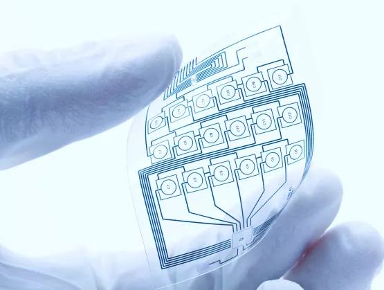
Peel-and-stick simplicity isn’t just for adhesive bandages any more. IoT and flexible hybrid electronics (FHE) are bound to change hardware business models. And flexible displays will breathe life into any surface.These were among the insights foreshadowing the future of the FHE, electronic textiles, IoT, MEMS and sensors industries at the FLEX Japan and MEMS Sensors Forum Japan 2018. At the April event, organized by SEMI-FlexTech-MSIG, nearly 200 attendees shared their observations and lessons learned in the development of processes, products and applications. Presentations and discussions revealed these five takeaways.1. Expect the unexpected with FHE developmentFlexible Hybrid Electronics (FHE) continues to shrink the size and weight of products, enabling new markets and concepts. “FHE takes printed electronics and adds ICs for getting performance out of the PE structure,” said Wilfried Bair of NextFlex, adding that “peel- and-stick electronic products are one example of unexpected new markets enabled by FHE capabilities.” One potential application is large peel-and-stick safety sensors adhered to buildings to warn of structural dangers.Another surprising turn: With new insights into OLED technology originally developed for flexible displays, Cambridge Display Technology (CDT) has devised an innovative medical diagnostic tool for markets such as biomedical and agricultural monitoring. The tool features an atmosphere-processable OLED component with a simplified OLED structure encapsulated in aluminum foil.2. IoT and FHE devices should change hardware business modelsThis is the standard business model for many new FHE products: develop a product, manufacture it, find customers and sell. FHE and IOT device developers were encouraged by Jam Kahn of Gemalto to consider flipping the script: During FHE product development, explore building an after-market revenue stream by controlling and mining the data for trends it reveals. Because of its data harvesting potential, IoT is an excellent emerging technology for this strategy.The “Experience Economy” could create 200 connectable items per person, generating strong revenue streams from the collection and analysis of massive amounts of sensor-generated data. The key is for the data to be actionable. That means hardware suppliers must extend their focus to software development. “A recent study of California investors found that by 2025, 60 percent of global business profits will be from data,“ noted Harri Kopola of VTT, who advised hardware producers to examine business models that produce continuous value by leveraging software. “With FHE, we are creating the path to digitization for non-digital industries, and these industries need complete solutions,” he said.Hardware provider Xenoma, for example, sells an electronic shirt with sensors for measuring muscle movements, heart rate and other health-related data. Xenoma’s Ichiro Amimori said the company offers its open-source software development kit for free under one condition: The developer must share the collection data with Xenoma. The idea is that the more data collected, the greater Xenoma’s ability to improve human health over the long term and achieve its long-term vision of alleviating disease.3. Roll-to-roll and sheet-to-sheet manufacturing will meet in the middleOne of the big advantages of flexible and printed electronics was its promise to enable the manufacturing of electronics on a roll-to-roll (R2R) process in atmospheric (or close) conditions, like newspaper, rather than one sheet at a time, as with displays or wafers. But as development of inks and interconnects progressed, along with the placement of discrete and thinned-die components and basic flexible substrates on a moving web, most research and development (R D) and limited-production runs moved to sheet-fed systems to control material costs for experiments and low-volume production. R D on printing electronics processes split into two camps: the simple printed components camp on R2R, and the camp backing more flexible hybrid electronics development on a sheet-by-sheet basis. But progress didn’t stop.Harri Kopola of VTT highlighted new R2R inspection and test capabilities in the VTT pilot line in Finland. R2R processing advances incorporate ideas from biology, chemistry, optics, optoelectronics, advanced inspection and test capability, illustrating the multidisciplinary nature of FHE. While accurate, high-speed, pick and place of thinned, bare die remains the domain of sheet-to-sheet manufacturing, look for more improvements in accuracy and speed.Another new manufacturing concept that turns business models on their heads – “minimal fabs” – focuses on creating limited-run equipment and processes that use 3D printing and do not require cleanrooms. With a relatively low cost of entry, the approach enables electronics to be produced affordably anywhere.4. Powering the IoT is a grand challengeThe requirement for edge devices to function without intervention for long periods raises hard questions about how to power the devices. Using organic photovoltaics (OPV) in textiles to harvest energy from light could be one solution, according to Kasimaesttro Sugino of the Suminoe Textile Technical Center. ULVAC’s answer to the IoT power issue are requirements for edge device micro-batteries to be environmentally benign, safe, flexible and compatible with semiconductor processing less than .1 mm in height. The micro-batteries must also feature a long life and support continuous power output, high power density, low self-discharge (over 10 years) and mass production, said Shunsuke Sasaki of ULVAC. The batteries are being built on silicon, glass and stainless steel with dry, thin-film vacuum processing. 5. Flexible displays bring any surface to lifeWith their durability, flexibility, low-cost processing and programmability, flexible displays can transform any surface into a content-rich display with messages that make lives healthier, simpler and safer.One example is FlexEnable’s organic thin-film transistor (OTFT), a device made possible not only by recent advances such as the ability to build organic material transistors on plastic and the increasing clarity of new film materials but by continuous manufacturing process improvements. These advances are improving switching times and the color and video capabilities of thin-film transistors while retaining their flexibility, low power consumption and communication capabilities. Simon Jone of FlexEnable gave the examples of wrapping a display around the blind spots of automobiles or replacing side-view mirrors with interior monitors showing feeds from an external camera, approaches that would improve safety while reducing wind drag and increasing fuel efficiency.E Ink’s reflective technology and flexible products are coming to market with a wider color spectrum. The company’s Michael McCreary said its designers are specifying the panels for innovative projects such as the exterior walls of the San Diego International Airport parking garage. Used to communicate with airport visitors, the installation is weather-proof, programmable and self-powered.
Read More
Enjoying the richest lineup of talent and resources in SEMI history, West isn’t just a show anymoreIt’s a powerful conversation. With new venues, new voices, and new takes on the industries and markets that will fuel the industry’s growth, SEMICON West is adding more value and taking a fresh approach to event experiences.Arrive smart, advance to “beyond smart.” That’s AI we’re talking about, and you’ll see demos on how it’ll enhance every one of our established and emerging markets. TechXPOT pavilions will be ground zero for discussing the freshest perspectives about autonomous and connected transportation and smart manufacturing. Designed exclusively to increase your expertise in the most promising areas for the next five years of industry growth, the featured interactions will center around innovations for improving data sharing across the global supply chain.Meet the experts. They’ll be waiting for you at the Meet the Experts Theater in the Smart Manufacturing and Smart Transportation Pavilions located on the show floor. Placed specifically for your easy access, the experts represent the top of their fields in emerging IC technologies for leveraging connected intelligence in electronics manufacturing. They’ll drive conversations about the hottest areas of growth opportunity and how to crack the challenges facing the industry. They look forward to the specifics that you want to explore. “Workforce development” has become a rallying cry. Coming off a banner year, the chip business is mounting an unprecedented recruitment drive to attract the best talent. The results are vital for the next state-of-the-art tech roadmaps that rely on the most intelligent minds. To help accelerate learning curves, the Smart Workforce Pavilion welcomes college students and recent grads to see the engineering pros discuss what it’s like to work in the microelectronics industry, and to gain an understanding about what technologies will be driving the future.As an engineer and executive, I’ve attended SEMICON West for 25 years – this year’s event raises to another level the value of content and networking for all. Let’s talk at the show. We want to hear your ideas about how we move beyond smart to even higher growth and innovation.Register today for an Expo Pass to tour the exhibition floor and gain access to the Smart Pavilions and Meet the Experts Theaters. Or choose the Thought Leadership or All-in Pass to receive access to the TechXPOT presentations and more. To view all conference pass benefits, visit www.semiconwest.org/pricing.Great products start with semiconductors. Conversations make them happen.
Read More
Just as the annual Cherry Blossom festival wraps up, international trade has flowered as a top concern for SEMI members, requiring immediate action as 20 SEMI member executives carried the torch for the industry in recent meetings with lawmakers at the annual SEMI Washington Forum. The business leaders quickly zeroed in on the proposed Sec. 301 tariffs of 25 percent on China imports to the U.S. and their potential to drive sharp increases in the cost of doing business. In the meetings at the two-day event in Washington, D.C., the executives expressed deep concern that the tariffs, aimed at protecting the interests of U.S. companies, would instead harm the intended beneficiaries including SEMI members around the globe. The executives also focused on the proposed 232 tariffs on steel and aluminum that would compound the damage to their businesses, spiking costs of materials that lie at the heart of their manufacturing operations. Also crucial to their business interests, the SEMI members educated lawmakers on the talent shortage and the intense competition to fill open positions across the supply chain. With fully 77 percent of industry executives seeing talent shortfalls as a pressing business issue, the business leaders pushed for legislation that would bring more domestic talent into the STEM education pipeline – such as S. 1518, The CHANCE in Tech Act to support more apprenticeships in technology, and H.R. 4023, the Developing Tomorrow’s Engineering and Technical Workforce Act to get more students involved in engineering. The group also encouraged support of the “Immigration Innovation” or “I-Squared” bill to strengthen and expand the H1-B visa program and STEM Greencards. The SEMI Washington Forum, a venue for SEMI members to educate lawmakers about the industry, also addressed concerns over restrictions on foreign investment in the U.S. Passage of S. 2098, the Foreign Investment Risk Review Modernization Act (FIRRMA), would usher in new operating efficiencies for the Committee for Foreign Investment in the United States (CFIUS) by adding much-needed resources to the overburdened body. However, the bill would also subject many ordinary business transactions to a lengthy and costly national security review that would hamper the ability of many companies to do business in the global marketplace. All told, attendees at the forum held more than 30 meetings with lawmakers, reflecting the great impact of public policy on SEMI members companies. In a time when the stakes for the industry have risen to new levels, direct engagement with lawmakers in the nation’s capital by SEMI and its members is critical. The SEMI Washington Forum is a terrific way for members to more clearly understand the impact of key pieces of legislation and gain firsthand experience in influencing policy and helping lawmakers better understand the industry. If you are interested in learning more about the SEMI Washington Forum or SEMI’s public policy program, please contact Jamie Girard by email at [email protected].
Read More
2017 was a record-breaking year for the semiconductor industry. At SEMI, our aim is to help our members continue that momentum. To accomplish this goal, we need to encourage thousands more engineers, technologists and innovators to join our exciting industry.SEMI president and CEO Ajit Manocha has stated, “Attracting new candidates to build a global workforce is critical to sustaining the pace of innovation. If we don’t act together, we’ll limit our growth.”To meet the challenge, SEMI recently launched a workforce development initiative, a key pillar of SEMI goals to support our member companies. The showcase for meeting this challenge is the first-ever Smart Workforce Pavilion—an innovative talent recruitment venue making its premier at SEMICON West 2018 in July. The Pavilion represents a unique opportunity for SEMI member companies to get involved in an initiative that is critically important to our industry’s future success. The Smart Workforce Pavilion will connect a diverse audience of promising, entry-level prospects with SEMI member talent acquisition and human resources (HR) recruiting teams. The Smart Workforce Pavilion offers a variety of ways to engage with college students seeking to enter our industry’s Smart Workforce. Members who engage at the higher levels will have an opportunity to:connect a diverse audience of promising, entry-level prospects with SEMI member talent acquisition and human resources (HR) recruiting teams. Staff a booth within the Pavilion, where your HR representatives can informally meet with entry-level prospects to review resumes, conduct informational interviews, or even begin the application process. List some of your company’s open, entry-level positions on the onsite job board. Sign up to learn more about participation in a formal mentoring program. Provide your company literature and recruitment materials within a college student resource kit. Deliver motivational “day-in-the-life” presentations on how to pursue a career in the industry and why your company is the place to begin.* The Smart Workforce Pavilion promises to be a major draw at SEMICON West 2018. Join this effort and bring your voice to celebrate our industry as you seek new talent for your company. Start today! Contact Shane Poblete at +1.202.847.5983 or [email protected] *Featured benefit listed is only available to the highest-level participants.
Read More
SEMI’s mantra is: Connect, Collaborate, Innovate. This mantra has delivered industry-enabling value to our members since SEMI’s beginnings in 1970. It has been essential for SEMI members to grow and prosper locally, while being synchronized globally. As the electronics manufacturing business has become more complex and interdependent, SEMI’s mantra has increasingly been applied across the full span of electronics manufacturing.With the IC industry now worth over $400 billion in annual revenue, developing a single new chip can cost hundreds of millions of dollars. Consequently, industry players now connect, collaborate, and innovate in new, but more often, deeper ways. This is especially true with IC design – what’s possible in chip design is only possible if the manufacturing processes can be developed as projected. It makes sense, as complexity grows and the stakes get higher, that design and manufacturing are closely linked and apply the SEMI mantra together. Where Electronics Begin“Where Electronics Begin” is the tagline of the Electronics System Design Alliance, or the ESD Alliance. It aptly distills the fact that all IC manufacturing begins with design – and the design ecosystem. This week, SEMI announced it reached an agreement with the ESD Alliance to join SEMI as a SEMI Strategic Association Partner. The ESD Alliance will become part of the SEMI organization in 2018. With the ESD Alliance and its community joining SEMI, its membership will complete the full electronics design and manufacturing span.This is a momentous step forward. The ESD Alliance’s ecosystem is vital and thriving and includes the world’s leading EDA and IP companies. Within the ESD Alliance community, Aart de Geus (Synopsys), Wally Rhines (Mentor, a Siemens Company), Simon Segars (Arm), and Lip-Bu Tan (Cadence), among others, are already familiar figures, having brought their thought leadership to SEMI platforms in the past. Now they, and the rest of the ESD Alliance members, will be able to more directly work with semiconductor equipment manufacturers, devices makers, and the rest of SEMI’s membership.At events like SEMICON China, which recently concluded in March and attracted over 90,000 attendees, SEMI and the ESD Alliance members will be able to efficiently connect and engage the supply chain players and find new areas for collaboration. As SEMI’s membership looks out towards new applications and systems opportunities, having both ecosystems together will find possibilities faster and innovate approaches more practically. The ESD Alliance will maintain its distinct community identity and governance while having access to, and the ability to augment, SEMI’s global platforms including seven regional offices, programs and expositions (including SEMICONs), advocacy (including trade, tax, talent, and technology), industry research and statistics, and other SEMI Strategic Association Partner and technology communities.SEMI will gain direct access to the electronics design ecosystems to provide a deeper and wider value – to its combined membership – with SEMI’s mantra. SEMI and its more than 2,000 corporate members and more than 1.2 million stakeholders look forward to connecting, collaborating, and innovating with the ESD Alliance and its members. SEMI’s global reach and wide span of membership with ESD Alliance’s deep expertise in design and IP is truly the best of both worlds for all stakeholders.Connect: Design ManufacturingSEMI’s members have been reaching into the electronics design ecosystem and the ESD Alliance members have been reaching into SEMI’s ecosystem to optimize design and manufacturing process for lowest cost and highest yield. This week’s announcement is a step forward to directly and more intimately connect electronics design and manufacturing for the supply chain to work more closely together in full synchronization. Collaborate: From Beginning to End in Electronics ApplicationsWith the ESD Alliance joining SEMI as a Strategic Association Partner, SEMI members can better collaborate across the full supply chain. Gone are the days when it was enough to collaborate only with one’s direct customer. Today, for example, components and c-subs suppliers frequently collaborate not just with their OEM equipment manufacturer customers, but with device manufacturers – and even system integrators. To be successful, companies are striving for connection to their customers’ customers.The ESD Alliance, with its design ecosystem and linkage to the fabless community, will join three existing SEMI Strategic Association Partners: Fab Owners Alliance (FOA), MEMS Sensors Industry Group (MSIG), and FlexTech (the association representing the flexible hybrid electronics ecosystem). These relationships now cover the entire span of electronics manufacturing.To provide focused collaboration across the full supply chain, SEMI has developed five vertical application platforms: IoT, Smart Manufacturing, Smart Transportation, Smart MedTech, and Smart Data. These have been chosen because of unique and pressing needs to synchronize the supply chain and to engage and develop solutions collectively.Innovate: Faster FutureWith the confluence of emerging digital disruptions and new demand drivers, forecasts suggest the IC industry could grow to over $1 trillion in annual revenue by 2030. To deliver this growth, the supply chain must efficiently innovate together. SEMI’s value proposition is to speed the time to better business results for its members across the global electronics (design and) manufacturing supply chain. The addition of the ESD Alliance as a Strategic Association Partner is a key contributor to deliver this value proposition for the industry to grow and prosper now and in the future.
Read More
Although many months past due, Congress on March 23 finalized the federal spending for the remainder of fiscal year (FY) 2018, only hours before a what would have been the third government shutdown of the year. Congressional spending has been allocated in fits and starts since the end of FY 2017 last September, with patchwork deals keeping things running amid pervasive uncertainty. While this clearly isn’t an ideal way to fund the federal government, the end result will make many in the business of research and development pleased with the addition of more resources for science and innovation.There was grave concern over the future of federal spending with the release of the president’s FY 2018 budget, which would have cut the National Science Foundation (NSF) budget by 11 percent and National Institutes of Standards Technology (NIST) spending by 30 percent. Relief came with early drafts from Congress that whittled those cuts down to between 2-9 percent. But the real boost was a February bipartisan Congressional agreement that lifted self-imposed spending caps and introduced a generous dose of non-defense discretionary spending, increasing NSF spending 3.9 percent over the previous year and the NIST budget an astounding 25.9 percent over FY 2017 levels.SEMI applauds this much-needed support for basic research and development (R D) at these agencies after their budgets were cut or flat-funded for multiple cycles. It is well understood that federal R D funding is critical to U.S. competitiveness and future economic prosperity. With the stakes that high, full funding of R D programs at the NSF and NIST should be a bipartisan national priority backed by a strong and united community of stakeholders and advocates in the business, professional, research, and education communities.With the work for FY 2018 completed, Congress will now turn to FY 2019 spending – already behind schedule due to the belated completion of the previous year’s budget. With 2018 an election year, Congress will likely begin work on the FY 2019 budget in short order, but probably won’t complete its work prior to the November elections. SEMI will continue to work with lawmakers to support the R D budgets at the agencies and their important basic science research. If you’d like to know how you can be more involved with SEMI’s public policy work, please contact Jamie Girard, Sr. Director, Public Policy at [email protected].
Read More
A Communication ProblemAs the industry ventures towards a more connected world, the semiconductor test community is facing increasingly stringent performance, quality and reliability targets, particularly in the high-stakes automotive, communications, and medical sectors. It is, therefore, important for device makers to know how their components will perform before their products hit the road, reach for the skies, or get placed inside the body. Access to test data is critical to mitigating failure risks. Yet many challenges are associated with accessing test and manufacturing data. One hurdle is that component suppliers are often reluctant to provide test data for fear of revealing sensitive information about their design and/or manufacturing IP. With customers sourcing their components from multiple vendors, IP leakage is a valid concern and, consequently, a barrier to access. Certainly, these issues can be negotiated contractually, but only after striking the delicate balance between access and cost. Beyond access, the quality of test data itself – which can be fragmented and even corrupted – is not always assured. As a device moves through the typical product flow (i.e., fab to sort to assembly to test), it inevitably changes hands (e.g., from foundry to OSATs). As a result, information about the device can become a patchwork of data where formats vary and certain fields, at times, may get overwritten. These potential gaps in test data flow underscore the need for consistent communications of manufacturing information from one process or stakeholder to the next. While standardization could help, it is currently lacking in many of these critical data-flow chains in the manufacturing, test, and assembly areas. An Industry Alliance Aimed at Solving Test Industry ProblemsEfforts to establish standardized solutions to these test industry issues are under way by the SEMI Collaborative Alliance for Semiconductor Test (CAST) Special Interest Group. CAST activities are currently structured around establishing standards on data formats, communication protocols, and chip traceability.Rich Interactive Test Database (RITdb)While Standard Test Data Format (STDF) is widely used in the semiconductor industry, it does not directly support the new use models in today’s test environment, such as real-time or pseudo real-time queries, adaptive test and streaming access. The STDF V4 record format is not extendible and, because the standard itself can be imprecise, it tends to result in many interpretations. These limitations become apparent when there is a need for more efficient and flexible format to manage “big test data.”The RITdb group has been working on the next-generation format following STDF to allow more flexibility in data types and support for adaptive test. The group aims to provide a standards-driven data environment for semiconductor test including simple standards-based data capture, transport and relationship model for eTest, probe, and final test data. Its work also seeks to support equipment configuration management and operational performance data. More importantly, RITdb enables a real-time streaming model that provides the ability to collect and monitor data/systems from sand to landfill.Real Time Adaptive Test (Courtesy HIR)Work by the RITdb group will ultimately be developed into SEMI Standards. The SEMI Standard spec will be in MS Word while the database itself in a different format. A spec editor will help ensure it is used correctly. The group also plans to expand the spec beyond probe and final test. Meanwhile, the group is working to streamline RITdb and implement different extensions (e.g., tester log, streaming). Additional work will be needed on probe maps and test cases (i.e., be able to run verifiers to validate the spec).Tester Event Messaging for Semiconductors (TEMS)Today, semiconductor testing continues to see a surging demand for real-time data analysis, real-time ATE input and control of the test flow to improve test yield, throughput, efficiency, and product quality. At the same time, test equipment and test operations around the world use a diverse range of data formats, specifications, and interface requirements that drive up customer service and application engineering costs for ATE vendors, OSAT companies, IDM test operations, software providers, and handler equipment. A common ATE hardware and software communications interface would help reduce the cost, time and complexity of integrating ATE equipment into data-intensive test operations.Overview of Test Cell CommunicationThe TEMS group was chartered to develop a standardized ATE data messaging system based on industry-standard internet communication protocols between a test cell host and a server. The standard will be limited to ATE data messaging, using RITdb entity types as applicable, standard data format, and control requirements. It will have no impact on other test communication interfaces such as those involving handlers, probers, test instrumentation, and other systems covered by existing standards (e.g., SEMI E30, E4, E5, STDF). The group is developing a set of standards to define a vendor-neutral way to collect test cell data. The primary spec defines the model while a subordinate spec defines the transport layer to maintain consistency with prior standards.Chip ID TraceabilityChip ID Traceability is the most recent group formed under CAST. The group’s formation came on the heels of the 2017 CAST Workshop that focused on Component System Level Test. SLT is widely considered a burden that most chip manufacturers prefer to avoid, but it is essential to achieving lower DPPM (Defective Parts Per Million) goals at system level. The cost to develop and maintain SLT equipment in-house and at OSATS is significant. SLT test engineering requires different skills than regular ATE test engineering. The engineers must understand the final application environment and the data flow that is subjected to the component. Defect causes need to be isolated and communicated back to the vendor or ATE test engineer for corrective action. Mapping such SLT failures back to the ATE production tests is a big, labor-intensive challenge.Component traceability is a big concern. Most newer technologies have ECID (Electronic Chip Identification). However, many product types representing significant volumes do not provide ID traceability. Without component-level traceability, it is extremely difficult to analyze failures and drive corrective action. Additionally, there is basic manufacturing data, including chip ID, that is needed across the supply chain, but this is often blocked and difficult to obtain from suppliers. Such data analysis is difficult across "silos" due to sharing/security barriers. Die-level Identification Traceability (I T) ModelThe Chip ID Traceability group was chartered to develop a standardized approach for enabling traceable die-level identification (ID) throughout the IC manufacturing, test, and assembly processes to the point of use in the final system. The approach defines the use of a simple, unique identifier that IC suppliers and board-level manufacturers can use to communicate about a specific device for the purposes of performance or failure analysis. The identifier will enable suppliers and customers to communicate specific component information and, with NDAs (non-disclosure agreements) in place, send manufacturing data back and forward through the supply chain for data analysis. The group is developing a standardized model focusing on key concepts, behaviors, and requirements for enabling die ID and traceability. The model defines minimum chip ID and traceability for new design and manufacturing implementation as well as for backwards compatibility with existing methods. The resulting standard would apply to different chip configurations ranging from single integrated circuits to multi-chip/3D structures. It can be adapted for use with a range of technologies, ranging from legacy systems to the latest in electronic chip identification (ECID). A copy of the draft proposal can be downloaded here. The Chip ID Traceability group is soliciting feedback to the document. Please contact Paul Trio at SEMI ([email protected]).

Read More
With less than one week before ISS Europe 2018, 4-6 March in Dublin, Ireland, industry growth is on the minds of the leading industry analysts, researchers, economists and technologists who will come together for critical insights into the forces shaping the electronics manufacturing supply chain.The three-day flagship business conference will feature a panel discussion on the role of Europe in the global electronics manufacturing supply chain and related business and technology trends. The Day 2 panel discussion will home in on critical strategies for growing Europe across the supply chain and elevating the region’s influence in Artificial Intelligence (AI) and other potential enablers of European competitiveness and technology leadership.SEMI Europe caught up with two industry leaders presenting at ISS Europe 2018 for their insights on technology and talent – two pillars of future industry expansion.Google: AI, Machine Learning and Ethical SolutionsDavid Sneddon, Director of Large Customer Sales for Central EuropeSEMI: As a Director of Large Customer Sales for Central Europe what is your primary focus? Sneddon: Right now my focus is mainly on advertising and marketing sales. For instance, I look after the advertising reviews for Google and YouTube for the DACH/CEE region. Our team offers both digital marketing advice as well as advice on logistics, translation of advertising and web assets, localisation of web/app assets and payment solutions.SEMI: What do you think are going to be the main challenges for the industry in the next two years?Sneddon: I think our industry will face two main challenges. For the technology industry as a whole, and in particular for the advertising sector, the first challenge will be to recognize the perception of the growing power of technology. Google, Facebook, and other big players should work closely with governments and regulatory officers in order to build trust. This is gaining importance within today’s users and leaders should commit to building trust. A second challenge is related to the growing importance of big data, AI and machine learning: industry players should be able to develop useful technologies but, most of all, ethical solutions.SEMI: Industry wide, what work/technology/trend has excited you this year? Sneddon: Innovations in machine learning and AI show how much machines can do to improve our daily life. Think about how Google Translate has developed. The first version was not so accurate but since the introduction of Google Neural Machine Translation system (GNMT), which takes advantage of deep neural networks, translations and sound are more accurate. If 2017 was huge for advancements in artificial intelligence and machine learning, 2018 may deliver even more. SEMI: What do you expect from ISS Europe strategic discussions and why would you recommend attending the event? Sneddon: I am attending SEMI ISS Europe for the first time and expect to hear peers’ high-level debates on the future of the industry, to be inspired and contribute myself. Top industry players should attend this event to stimulate the exchange of strategic discussions around innovation and technology. The key message that we, as leaders of this exciting industry, should deliver refers to the ethical aspects I have mentioned before. It is up to us to be prosperous and ethical at the same time and deliver positive messages for the year ahead. CEI-Europe AB: Smart Training for Smarter EngineersAnn-Charlotte Johannesson, CEOSEMI: As a CEO for CEI-Europe what is your primary focus?Johannesson: At the moment, my main focus is to refresh our approach in e-learning. CEI-Europe has organised classroom courses since 1980. We see now that there is a major need for e-learning courses and digital platform, so this is what I have been doing recently. Very soon a new website with a refreshed look and feel will be available.SEMI: What do you think are going to be the main challenges for the industry in the next decade?Johannesson: The industry must keep employees educated to keep them motivated and happy. As we all know, there is a lack of engineers in Europe. Fewer people are doing more work and, as a result, there is less time to stay on track with innovations, updates and trends. The investment in learning is happening but it is not enough. The industry’s main challenges will be: How do I train my team? How do I attract new people? Traveling to attend courses might be expensive and time-consuming, but a good alternative is to set targets for the training, learn what your company needs and offer individualized solutions. This is the way to prosper and stimulate people working in a fast-growing industry.SEMI: In what ways do you think the industry can change for the better?Johannesson: When it comes to education, it’s important for businesses to see it as an investment, not merely a cost. Think about the future, and invest in the future.SEMI: What do you expect from ISS Europe strategic discussions and why would you recommend attending the event?Johannesson: I’ve collaborated with SEMI a long time and am excited about presenting our perspectives for the future. I expect to meet and network with key leaders and discuss the main challenges for Europe and how to overcome those. How do we train smarter engineers? See you in Dublin!The combination of insightful presentations and unparalleled networking opportunities amongst senior industry leaders at ISS Europe promises to help stimulate ideas and strategies to take advantage of the opportunities that are rapidly developing in our industry.For full program details, please visit the ISS Europe 2018 agenda page online. To register, please visit: semi.huihuidehui.workers.dev/eu/iss-europe-2018-registration
Read More
In my first six months at SEMI, I’ve visited with many member companies and industry leaders. One theme I hear repeatedly is a concern about our most fundamental source of innovation and productivity – people.Our industry has a significant need for additional workers and several trends are working against us.For one, only 11 percent of elementary students in the U.S. indicate an interest in science, technology, engineering, and mathematics (STEM) education according to the National Science Foundation. In other regions, recruiting and retaining high-skilled workers remains a constant challenge.Ironically, the incredible electronics manufacturing technology that we create has enabled many of the new-tech industries in software, social media, internet services and applications that now directly compete for the best and brightest technical talent. Young engineers have other choices and many are lured to newer growth industries with familiar internet brands.Today, due to continued industry advancement and robust growth, capital equipment companies, device makers and materials companies collectively have thousands to tens-of-thousands of open unfilled positions. Furthermore, the representation of women in the high-tech workplace remains disproportionately low.We have long been aware of the need to support a diverse pipeline for high-skilled workers. In 2001, the SEMI Foundation was established to encourage STEM education and stimulate interest in high-tech careers. SEMI and its Foundation launched the High-Tech U (HTU) program to engage and excite high school students. HTU enlists industry volunteers to work with local high school students in a three-day interactive hands-on curriculum. Young people get a fun and inspirational exposure to binary logic, circuit making, a fab or electronics manufacturing setting and other aspects of professional development.To date, we’ve delivered 216 HTU programs and reached nearly 7,000 students in 12 states and nine countries. The results are compelling. Our 2016 survey of HTU alumni shows that they enter college at five times the national rates and 70 percent that graduated college are employed in a STEM field. By any measure, the initiative is successful and worthwhile.However, the talent problem statement has grown. Industry needs are greater and the time has come to redouble our effort to attract and retain talent for our high-skilled manufacturing sector. Therefore, SEMI is elevating workforce development as a top strategic priority.The SEMI HTU team is already engaged with key member companies to develop our enhanced roadmap for workforce development including a comprehensive study with Deloitte Consulting to underpin the key problems and solutions in areas of focus for decisive and systematic SEMI action.Belle Wei, SEMI Foundation Board member and the Carolyn Guidry Chair in Engineering Education and Innovative Learning at San Jose State University said, "It is critical that we work to prepare the future workforce. This requires a high level of collaboration between industry and higher education. We appreciate SEMI's leadership role in this collaboration to further develop the workforce pipeline."We have launched a HTU Certified Partner Program (CPP) with the goal of reaching more students through industry partners who commit to long-term participation and independent delivery of High Tech U. In addition, we are expanding outreach to universities and community colleges and preparing to launch an industry image campaign to better tell the remarkable story of opportunity in our industry.The capacity to innovate and the skills to manage complex design, engineering and manufacturing processes are essential factors that sustains our high-tech industry – and they are dependent on people.Finally, as mentioned above, we have already started some new initiatives to enhance our HTU. A SEMI workforce development roadmap and execution plan will be detailed in a future SEMI Global Update article following the upcoming SEMI International Board Meeting. SEMI welcomes any inputs in addition to your continued support.This endeavor is increasingly urgent and recruiting the industry’s future innovators is well-aligned with SEMI’s mantra to connect, collaborate, innovate, grow and prosper.
Read More