downloadGroupGroupnoun_press release_995423_000000 copyGroupnoun_Feed_96767_000000Group 19noun_pictures_1817522_000000Member company iconResource item iconStore item iconGroup 19Group 19noun_Photo_2085192_000000 Copynoun_presentation_2096081_000000Group 19Group Copy 7noun_webinar_692730_000000Path
Skip to main content
Default Banner Image

Technology and Trends

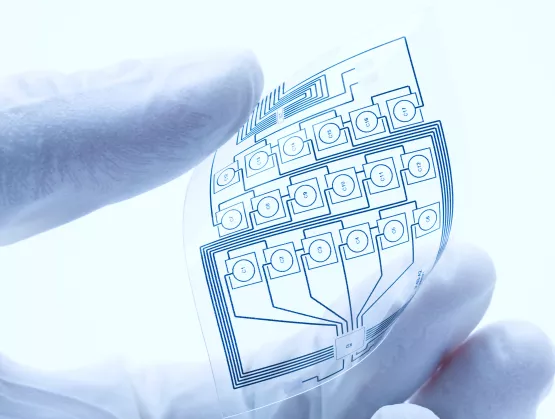
A multidisciplinary team of researchers is developing new methods to collect and analyze sweat for clues about how the body is functioning.Imagine if you could know the status of any molecule in your body without needing to get your blood drawn. Science fiction? Almost – but researchers at the University of Arizona are working on ways to do this by measuring molecules in sweat.When physicians take blood samples from patients, they send the samples to labs to be analyzed for biomarkers. These biological clues indicate everything from cholesterol levels to disease risks, and they can be used to monitor patient health or make diagnostic decisions. The same biomarkers also are found in sweat.Using $519,000 in funding from SEMI-NBMC (Nano-Bio Materials Consortium), Erin Ratcliff, University of Arizona materials science and engineering professor and head of the UArizona Laboratory for Interface Science of Printable Electronic Materials, is leading a project to develop new ways of collecting and analyzing the clues sweat has to offer. Ultimately, this work could allow physicians to use patient sweat samples in the same way they currently use blood samples, for a less invasive and more informative approach to establishing and monitoring patient health.“What’s unique about this is that we are combining biology and engineering expertise to develop a wearable device that will detect molecules in sweat, so you don’t have to get your blood drawn to know the health status of your immune system, your nervous system, indeed, any system in the body,” said co-investigator and sweat biomarker pioneer, Esther Sternberg, MD. “The goal, eventually, is to create a device that will provide physicians and health care providers the ability to monitor your health status continuously and in real-time without needing to draw blood.” Materials science and engineering professor Dr. Erin Ratcliff in her laboratory at the BIO5 Institute at the University of Arizona “We are pleased to sponsor and eager to complete this project with University of Arizona’s impressive team bridging the disciplines of engineering and life sciences,” notes Melissa Grupen-Shemansky, PhD, Chief Technology Officer and Executive Director of SEMI-NBMC. “A concerted interdisciplinary approach at the early stages of R D is relatively new and there is much learning on both sides. The UA team brings unique strengths in both areas and we are excited to be partnering and collaborating with them.”Ratcliff’s co-investigators are J. Ray Runyon, a research assistant professor in the Department of Environmental Science, and Sternberg, research director for the Andrew Weil Center for Integrative Medicine; director of the Institute on Place, Wellbeing, and Performance; and the Andrew Weil Inaugural Chair for Research in Integrative Medicine. Ratcliff and Sternberg are both members of the BIO5 Institute.Standardized Sample CollectionIn order to study sweat, researchers need to collect samples of it, and there are a number of ways to do so.“The obvious idea would be to make a patch that gets information from many pores at once, but the problem is that this creates a space between the patch and your skin, and you have to wait for it to fill up with sweat,” Ratcliff said. “We hypothesize that while you’re waiting, these molecules – the very molecules you’re trying to detect and analyze – are changing chemically.”The team’s first task is to develop new, continuous and hands-free collection devices that deliver high-quality, standardized sweat samples. This will allow health care professionals to gain a more holistic picture of a patient's bodily systems over an extended period, rather than the “snapshot” a blood draw can provide of a particular moment.Currently, sweat labs across the world are using different methods to collect samples, which limits researchers’ ability to compare data. Standardizing the collection method could provide researchers, including medical device developers, with a new degree of confidence in sweat sample data.“High-quality data, with respect to different target molecular biomarkers in sweat, requires that a high-quality sample be collected,” Runyon said. “This will be the first hands-free method that will truly take into account the interplay of the chemistry of sweat, the target biomarker and the device material.” University of Arizona student in classroom testing medtech devices Low-Level DetectionThe team is also developing methods for researchers to detect and analyze neuropeptides in the collected samples. Used by neurons to communicate with each other, these small molecules are involved in biological functions, including metabolism, reproduction and memory. Commercial wearable devices monitor metrics like heart rate, and some use sweat sensors to monitor dehydration level. Measuring neuropeptides, however, will allow researchers to zoom in millions of times closer to investigate stress and relaxation responses at the molecular level.“The idea is that your sweat is reflecting your nervous system – all of the neurotransmitters your body uses to signal between the brain and the rest of the body,” Ratcliff said. “Monitoring this biochemical response continually, over a 24-hour cycle, can inform us about the health of the wearer and also act as a diagnostic tool.”Meet Dr. Ratcliff and the University of Arizona team at FLEX in San Jose, Calif., February 23-26, 2020. Emily Dieckman is Editor at The University of Arizona. Republished with permission from the University of Arizona.
Read More
MEMS technology has changed human interaction with electronic devices. Introduced in the 1990s, the first mass-market MEMS devices were used for inkjet printheads and automotive airbag crash sensors. Today, MEMS are ubiquitous, with billions of the tiny devices adding intelligence and interactivity to smartphones, smart speakers, wearables, automobiles, biomedical devices, remote monitoring and event detection systems, and countless other applications. Integrating MEMS with Flexible Hybrid Electronics (FHE) is an important step in the evolution of this miniaturized intelligent sensing technology, paving the way for its use in new classes of flexible, conformal devices.The integration of the two technologies promises to breed new applications in small form factors but also presents challenges inherent to FHE design and fabrication processes. SEMI’s Nishita Rao caught up with Nathan Pretorius, prototyping and automation engineer, NextFlex, to discuss MEMS-FHE device integration challenges and opportunities ahead of his February 26 presentation, Integrating MEMS Devices in FHE, at FLEX|MEMS Sensors Technical Congress (MSTC) 2020, February 24-27, 2020, at the DoubleTree by Hilton in San Jose, California.Join us at FLEX|MSTC to meet Nathan and other industry influencers advancing innovation in FHE and MEMS sensors. Register now to connect with him at FLEX|MSTC or visit him on LinkedIn.SEMI: Why is integrating MEMS devices into FHE systems important? What new use cases might it enable?Pretorius: The main value proposition of integrating MEMS devices into FHE is that it allows MEMS devices to exist in a different form factor than was possible previously, giving us high-quality MEMS sensors on the flexible and conformable platform of FHE.Ease of application, flexibility, lower cost and rapid iteration on a design are just some of the benefits of FHE devices. And because there are few robust FHE sensors that overlap with MEMS’ capabilities, when you combine the two, you get a lot of compelling uses. That’s why NextFlex is working with agencies and companies to evaluate MEMS’ integration, including using bare MEMS die with microfluidics and promoting new ways of attaching and packaging MEMS die for use with FHE. SEMI: Why is FHE an ideal platform for integrating various types of sensors?Pretorius: MEMS integrated with FHE devices are ideal for rapid design and deployment of data-gathering sensor nodes — which we can iterate for specific applications. A few examples include on-body health monitoring devices for bio-fluids analysis, medical pressure sensors for monitoring blood pressure, and peel-and-stick sensors nodes for infrastructure monitoring. In terms of design and production, FHE devices support rapid prototyping, allowing for instantaneous design-iteration cycles. This speeds design-to-production over traditional rigid PCBs and copper flex because the feedback cycle time between design, manufacturing and testing is shorter, accelerating time to market. What’s exciting about FHE technology is that a variety of sensors or components, including MEMS, can be designed into the base system to easily customize it for a specific application. In addition, our experience shows that when compared to a traditional rigid PCB, an FHE board reduces manufacturing steps and device weight by two-thirds and, perhaps most importantly, converts the device to a thin, conformal shape that makes possible products in new form factors. SEMI: What are the primary challenges to integrating MEMS with FHE? What is NextFlex doing to help device manufacturers address these challenges? Pretorius: There are a few challenges, some of which are device-specific. Most recently, I’ve been focusing on inertial and timing devices, including accelerometers, gyroscopes and resonators. There are a few technical challenges involved in the process of getting the devices from the wafer to an FHE substrate. The wafer processing is very important, especially the dicing and thinning steps. After thinning and dicing, the die is placed onto the FHE substrate. The stresses caused by bonding to the substrate have to be understood and characterized. After placing the die, you then have a calibration step, which is normally performed after the device is packaged. With a MEMS die placed onto directly onto an FHE substrate, calibration then must be done.Finally, the device encapsulation is important, since on an FHE substrate the hard-to-soft material transition is very important to mitigate stresses to rigid component interfaces. We have also been looking at how to work with devices that have damping vents. Flexible encapsulants are inherently more permeable to gases and water vapor than hard encapsulants, so studying the encapsulation of MEMS devices on FHE is another area of interest. NextFlex has been working in a supporting role to evaluate best design practices and best attach and integration methods. In addition to our ongoing collaborative programs, NextFlex is developing the FHE manufacturing ecosystem to include system and component manufacturers and designers, product developers, and materials and equipment providers.SEMI: How do we facilitate closer collaboration between the FHE manufacturing ecosystem and MEMS suppliers such as MEMS device manufacturers, product developers, and materials and equipment providers?Pretorius: It’s important to include manufacturers early in the design process so we can identify challenges up front. That’s why NextFlex spearheads technology road-mapping efforts that include representatives from across the manufacturing ecosystem. We use the roadmaps to prioritize challenges that we can address effectively through collaboration, focusing the industry on solving problems through Project Calls that reveal integration challenges and results from real devices and that tell us how the materials and equipment actually perform with a real device.NextFlex keeps the information flowing, holding quarterly project update webinars to share results. As current devices are optimized for the process in which they will be used, we learn a lot from the project performers who make FHE system demonstrators — and we share that information with the member community. SEMI: Can you point to an example of a successful MEMS-FHE device integration?Pretorius: MEMS-FHE integration is still in the early stages, but we are working on several projects including a DARPA Seedling project for which we have integrated MEMS sensors into FHE systems for testing and evaluation. We plan to continue this work by integrating MEMS and FHE devices using methods that support mass production.SEMI: What would you like FLEX|MSTC attendees to take away from your presentation?Pretorius: We would like to see the FHE community work more closely with MEMS device manufacturers. For example, NextFlex often works with manufacturers to gain access to bare die, which is still a significant hurdle in making devices.The best way to speed things along is to get involved. We encourage FLEX|MSTC attendees to join NextFlex. As a prototyping and automation engineer at NextFlex, Nathan Pretorius explores new print methods for prototyping and automation using novel materials and processes. Pretorius currently focuses on how best to apply software scripting and machine learning to streamline FHE processes. Prior to joining NextFlex, he researched the strengths of roll to roll and screen printing on printed electronics designs, including capacitive touch interfaces, FHE passive component design, and antennas. Nathan holds a Bachelor of Science degree in Graphic Communications from Clemson University. FLEX|MSTC is organized MEMS Sensors Industry Group (MSIG) and FlexTech, SEMI technology communities focused on the growth of MEMS sensors and the flexible electronics supply chain, respectively.Nishita Rao is marketing manager for technology communities at SEMI.
Read More
The GAP9, GreenWaves Technologies latest IoT application processor -- which is being fabbed on GlobalFoundries 22FDX (FD-SOI) technology -- will be sampling in the first half of 2020, according to EETimes (read the whole article here). Mass production is slated for 2021. Greenwaves (which has been an SOI Consortium member for several years now) is a fabless semiconductor startup designing disruptive ultra-low power embedded solutions for AI processing in sensing devices at the very edge. GreenWaves marketing director Martin Croome told EETimes, “We are using the body biasing ability in FD-SOI to allow us to achieve even lower power consumption.” Compared to GreenWaves’ currently shipping product, GAP8 (which is on a 55nm bulk process), GAP9 reduces energy consumption by 5 times while enabling inference on neural networks 10 times larger. This is thanks to architectural enhancements and the move to GF's 22FDX semiconductor process. The new chip delivers a peak cluster memory bandwidth of 41.6 GB/sec and up to 50 GOPS combined compute power at an overall power consumption of 50mW. It enables customers to embed machine learning and signal processing capabilities into battery operated or energy harvesting devices such as IoT sensors in smart building, consumer and industrial markets and consumer and medical wearable devices. GAP9 was showcased at the last RISC-V Summit in San Jose (read the full press release here). [caption id="attachment_29061" align="alignnone" width="400"] GAP9 Block diagram (Courtesy: GreenWaves)[/caption] Some of the (many!) features include: 10 identical high performance, extended ISA, RISC-V ISA cores (cluster of 9 cores for compute-intensive tasks and a fabric controller core for control and communication) Dynamic voltage frequency scaling and automatic body biasing Multiple power states: deep sleep, deep sleep with retentive RAM, low activity, SOC on, SOC on cluster on Click here for a full GAP9 product brief.
Read More
VTT Technical Research Centre of Finland Ltd (VTT) has its sights set high. As a leading global research and development firm , VTT is out to produce bio-interfacing and biodegradable flexible hybrid electronics (FHE) devices that help tackle some of the world’s greatest challenges including environmental degradation and food scarcity.SEMI’s Maria Vetrano interviewed Antti Vasara, president and CEO of VTT Technical Research Centre of Finland, to preview his February 25 keynote, Beyond Flexible Hybrid Electronics: Biodegradable Electronics and Interfacing Bio+Electronics, at FLEX|MEMS Sensors Technical Congress (MSTC) 2020, February 24-27 at the DoubleTree by Hilton in San Jose, California. Join us at FLEX|MSTC to meet Antti and other industry influencers driving innovation in flexible hybrid electronics (FHE) and MEMS sensors. Register now to connect with him at FLEX|MSTC or visit him on LinkedIn.SEMI: What is body-interfacing electronics and what is your vision for bio-interfacing and biodegradable electronics?Vasara: Body-interfacing electronics have existed for decades. Developed in the 1970s, the wireless heart rate monitor is a good example. While continuous heart monitoring with a compact, inexpensive wearable device is widely accessible technology, other bodily parameters, such as cholesterol levels or biomarkers, are diagnosed every time we see a doctor. Establishing a baseline using multiple measurements — before symptoms develop is actually much more effective.That’s where bio-interfacing comes in. Bio-interfacing devices will continuously measure and analyze complex biogenic substances such as sweat, breath, blood and urine. A smart patch for continuous sweat monitoring, for example, would overcome several challenges: supporting electronics functionality in liquid environments, managing the transport of harvested samples to and from the sensor, managing potential contamination, and disposing of samples after measurement.While FHE in principle delivers the right building blocks and is an ideal form factor for a wearable sweat analytics patch, flexible circuits are not ready for out-of-the box interaction with biological matrices. Hence, our mission at VTT is to anticipate and develop the upscaling process know-how required for FHE devices that either interface with biological systems — or that must themselves biodegrade.We’re also focusing on biodegradable electronics because environmentally conscious end-users and manufacturing companies want biodegradable versions of energy-autonomous, label- or sticker-like Internet of Things (IoT) sensors. Typically used for packaging, logistics, environmental monitoring and medical diagnostics applications, these sensors — which have a lifetime of a few days, weeks or months — have become very popular. Unless they are biodegradable, however, they just add to landfill.SEMI: What approaches is VTT using to develop bio-interfacing and biodegradable electronics?Vasara: In our Business Finland-funded ECOtronics project, we are working with our partners to create recyclable and compostable electronics and optics that use renewable resources. For example, devices developed using substrate materials like paper, cardboard or VTT’s in-house-developed nanocellulose films and biopolymer films for environmental monitoring or skin patches can be easily recycled or even biodegrade naturally. Where possible, we use roll-to-roll printing to generate the device circuitry, and on a component level, we have optimized our assembly process towards bare-die component bonding to reduce the overall footprint of non-biodegradable waste per device.SEMI: What use cases do you find most promising and why?Vasara: A prominent example of a single-use test that generates a large amount of waste is the digital pregnancy test. When breaking it down into components, you will find a rigid circuit board with microprocessor, a couple of coin cell batteries, a liquid crystal display, a LED light source and photodiode, and a large chunk of plastic packaging around it. The materials and battery capacity of such a device would be sufficient to run hundreds of pregnancy tests – actually technical overkill.By using printed circuits on biodegradable substrates, bare-die assembled components (ASIC, LED light sources, photo diodes, thin film batteries as power sources) and device packaging composed of biodegradable plastics, we can completely redefine the environmental footprint of single-use tests. We are currently developing a toolbox for our customers to turn their existing conventional test into an ecotronic form factor.Another exciting use case is a sweat sensor that we developed collaboratively with Ali Javey, Ph.D., professor of Electrical Engineering and Computer Sciences, UC Berkeley, and the co-director of Berkeley Sensor and Actuator Center (BSAC). Together with his team, we created a wearable electrochemical sensor for continuous sweat analysis during exercise. With the UC Berkeley group providing the chemistry to monitor N+, K+ ion and hydration levels in sweat over the duration of several hours, VTT delivered the underlying sensor platform, featuring the printed sensor electrodes and sweat harvesting microfluidic channels for fluid management and transport. It’s exciting to see what we can achieve by combining techniques from different disciplines, in this case electrochemistry, printing, packaging and microelectronics.SEMI: How can industry enable the development/manufacture of flexible FHE devices? Where does VTT fit into the ecosystem?Vasara: As many FHE devices target large-volume markets, scalability of manufacturing is key: How can I get from one device (= working prototype) to a handful of devices (= feasibility study), to thousands (= pilot manufacturing), to a million (= mass manufacturing) without compromising the quality of the system’s performance and reliability?Access to upscaling infrastructure is essential for the development of novel FHE devices and methods, but infrastructure is expensive. That’s where our establishment of a roll-to-roll pilot printing line to bridge the gap between laboratory R D and mass manufacturing has proved invaluable. We can provide a unique worldwide upscaling infrastructure for advanced FHE devices, with a strong focus on large-area roll-to-roll processes and hybrid assembly. This service removes our customers’ burden of high infrastructure investment in early development stages and it allows us to guide customers along their development path, from prototype to mass production.Watch our video: VTT pilot manufacturing for diagnostics and wearablesSEMI: Is there anything else that device manufacturers need to know in order to succeed?Vasara: In my eyes, the success of FHE devices eventually depends on several factors: It requires a high degree of automation, well-optimized processes, reliable supply chains, and perhaps most importantly, clear standards and rules for designers to guarantee flawless interoperability of all the different elements on a flexible and hybrid circuit. Let us not forget – we are trying to marry electronics with printing, biology, packaging, microfluidics, injection molding and other fields of expertise.We recently finalized the compilation of a set of design rules for publication in our state-of-the-art overview of printed and hybrid electronics manufacturing methods. You can download the overview, PrintoCent Handbook, for free.SEMI: What would you like FLEX|MSTC attendees to take away from your presentation?Vasara: The latest technologies and innovations in microelectronics, MEMS, printing, materials, and biosensors provide us a toolbox for true innovation in the FHE space. Now we need cross-disciplinary thinking and daring steps to combine different manufacturing methods and skill-sets. The ideal cross-disciplinary team might include: The printing engineer who knows how to design contact pads for a bare-die IC assembly The biologist who knows about the thermal and mechanical stress in a printing environment to design processes for bio-functionalization of surfaces The electronics engineer who knows how to optimize a circuit powered with an enzymatic biofuel cell The number of sensors deployed on (or inside) our body, in our drinking water, in our cars, on our fields, in our pets, and everyday products will surely grow. Let us make sure they leave the smallest environmental footprint possible.Antti Vasara, Ph.D. has been the president and CEO of VTT Ltd since 2015. VTT is a visionary research, development and innovation partner with over 2000 people and a turnover exceeding 250M EURO. Vasara is president of EARTO (European Association of Research and Technology Organisations) and is chairman of the board of Palta (Finnish Service Sector Employers). In addition, he is a non-executive director of Elisa Oyj (largest communications operator in Finland) and a board member at EK (Finnish Confederation of Industries).He has served on several high-profile groups on industrial and innovation policy of the European Commission, in addition to several groups in Finland on artificial intelligence and research policy. Previously, Vasara spent close to 25 years in private industry, working at Nokia, Tieto, SmartTrust and McKinsey Company. Earlier in his career, he was a researcher in optical communications with 20+ peer-reviewed articles and one international patent. Vasara holds a Doctor of Science (Technology) degree from Aalto University in Finland.For more information about VTT’s work in bio-interfacing and biodegradable FHE devices, visit VTT Research. FLEX|MSTC is organized MEMS Sensors Industry Group (MSIG) and FlexTech, SEMI technology communities focused on the growth of MEMS sensors and the flexible electronics supply chain, respectively.Maria Vetrano is a public relations consultant at SEMI.
Read More
It should really be called SOI photonics – not just silicon photonics, quipped Soitec CTO Christophe Maleville at the SOI Consortium Japan event last fall. You’ve got to have SOI for the waveguides. There are megatrends driving significant growth in photonics – and they were all covered at the event. This is the final post in our coverage of the SOI Consortium’s Japan event (thank you for your patience!). It covers the photonics-related presentations by Soitec, Leti, Cisco/Luxtera, GlobalFoundries, Cadence and TowerJazz. Most of these presentations are now posted on the SOI Consortium website – you can access them if your organization is a member of the consortium. By way of reminder, the Japan SOI Symposium was a great success, with both days well attended. In case you missed our previous posts about the event, you’ll want to go back and read them, too. The first post covered the 5G/RF-SOI presentations by ST, Toshiba, Incize, GF, Silvaco and Sitri – you can read it here. The second post on the event covered eight very informative presentations on SOI in IoT and automotive by NXP, Dolphin Design, Leti, Silvaco, Arm, I-fuse and Secure-IC – you can read that here. Note that you can click on any of the illustrations to see enlarged versions. And now without further ado, here are the summaries of the photonics presentations. SOI Enabling Photonics – Ecosystem and Market Outlook – by Aziz Alami-Idrissi, GM Specialty SOI, Soitec. [caption id="attachment_28773" align="alignleft" width="233"] (Courtesy: Soitec SOI Consortium)[/caption] The megatrends in SOI photonics are: 5G (for more bandwidth, HPC, edge quantum computing), data centers (for high data rate transceivers and high-switch bandwidth), sensors (lidar, gas/chemical and gyroscopes) and biosensors (especially for medical). These are driving big changes: the 44% CAGR means the market is growing from a current TAM of about 500M$ to over 4B$ in 2025. One thing that’s really interesting is the expansion of the photonics market into these new fields in the next few years. While in 2019 90% of the photonics market served data center applications (the other 10% is for long haul), in 2025 optical I/O’s will account for over a third of the photonics market TAM. The other applications making an impact include AI, quantum, lidar (which will move into high-volume manufacturing in 2024) and medical sensors (hitting high-volume in 2023). For its part, Soitec is strengthening its portfolio with 8” and 12” large product coverage, new product sampling engaged, and extended features including newer engineered layers and RF immunity. Advanced Silicon Photonic Solutions Leverage SOI Technology – Eleonore Hardy, Business Development Manager, Silicon Photonics, CEA-Leti [caption id="attachment_28769" align="alignright" width="358"] (Courtesy: Leti SOI Consortium)[/caption] Leti helps companies make photonics products they can bring to volume foundries, explained Hardy. (btw, they’re presenting 21 (!) papers – including 5 invited – at PhotonicsWest 2020. Read about that here). You want to do integrated photonics to bring down costs, reduce power consumption, and scale (for higher volumes and reduced footprint). There are essentially three substrate choices: InP, SiN or SOI. SOI uses CMOS processes, so it’s low-cost and can be used in high-density photonic integrated circuits. What about the laser? Leti has developed III-V on silicon bonding, so you can have the laser on 4” III-V with a 300mm CMOS process (this is what Intel’s doing). They’re moving to 300mm wafers, 3D and advanced packaging. While communications is the big application realm, Leti is also applying photonics in automotive, medical, environment and computing. In the computing realm she gave the example of the European QuantERA SQUARE (Silicon Photonics for Quantum Fibre Networks) project for which Leti is doing the quantum emitter for absolute security and computing, wherein the transceiver/receiver for quantum cryptography integrates a hybrid III-V on silicon pump laser. Other examples of their work include miniature, low-cost and agile lidar for automotive and industrial applications (they’re working on a beam-steering emitter for an optical phased array). GlobalFoundries Silicon Photonics Solutions for Wired Infrastructure – Anthony Yu, VP, GF [caption id="attachment_28770" align="alignleft" width="684"] (Courtesy: GlobalFoundries SOI Consortium)[/caption] GF is giving their photonics business a big push. Optical interconnects are the future, said Yu, so they’re putting a lot of money into it. With data streaming multiplying by 3x/year and a current foundry TAM of $63 billion, the opportunity is huge. Fab 10 in Fishkill runs their 90WG process on 300mm wafers. A new process, 45CLO (also on 300mm) for O and C bands is going into the Malta fab. A big focus here are optical transceivers that convert RF signals to light. They see RF on SOI in a monolithic solution is needed to serve 100Gbs applications. They’re also moving to co-packaging optics: the packing technology will surround it with photonic chiplets. Customers have indicated that pulling the signals off the chips is limited by power, so they’ve worked hard on the fiber attach with MEMS and packaging technology for co-packaging. GF relies on substrate providers for high-quality SOI, and they have a world-class development team, he concluded. Integrated Electro-Photonics Design Platform – A multi-physics, multi-fabrics system design solution – Scott Li, Sr. AE Manager of Custom IC Platform, Cadence [caption id="attachment_28771" align="alignright" width="374"] (Courtesy: Cadence SOI Consortium)[/caption] This talk focused on photonics design challenges and solutions – including the CurvyCore™-based PDK for waveguide creation modal properties calculation that Cadence will soon be announcing. It’s a math-based engine that generates complex curvy shapes to support photonics. The first design challenges, said Li, are at the circuit level: how to do the schematics. The detailing tools, timesteps management and circuit simulation need to give the user the best performance. Cadence is working in close collaboration with a company called Lumericable on this. The next set of design challenges come at layout – especially generating curvilinear layout for any shape so that there are no gaps in connections. This is where CurvyCore comes in, fully automating layout and making it easy to modify. This includes place route, DRC and LVS for curvy shapes. The final challenge is at the system level. There is work to do here, but Cadence is collaborating closely on solutions with key partners. The ultimate goal is for photonics layout and editing to be available with all the features designers get in electronics editing. Silicon Photonics for High Volume and High Performance Optical Interconnects Applications – Thierry Pinguet, Technical Leader Engineering, Cisco /Luxtera [caption id="attachment_28772" align="alignleft" width="396"] (Courtesy: Cisco/Luxtera SOI Consortium)[/caption] Over the last decade there’s been steady growth in optical high speed interconnect solutions, mainly driven by HPC, enterprise, and especially the hyperscale datacenter. The largest volumes are for intra datacenter interconnect (between servers). Now mobile applications for backhaul are also driving volume for high speed optical interconnect for 5G network implementation. ASICs and photonics are getting closer as the industry moves to put them in the same package. But everybody does silicon photonics differently (even within Cisco). Luxtera tries to use the same infrastructure as electronics, but patterning is still a challenge: it’s not 90o “Manhattan” style. The wafers are no problem – they work with leading wafer suppliers like Soitec and SEH. They have explored a “double SOI” substrate (like a mirror), which showed large insertion loss improvements in grating couplers . For the electronics and the laser (MEMS), they do a micropackage, although at one point they also did monolithic integration. For better performance, they’re moving to TSVs. A hot topic is ASIC and photonics co-packaging. You can use optical tiles, but then the light is remote, like a power supply. No matter how you do it, though, the bottom line is that silicon photonics is the only way forward for the data center. PH18: World’s First Open Commercial Silicon Photonics Process and PDK from TowerJazz – Masanobu Kumazaki, Engineer, TowerJazz. This presentation was given in Japanese without translation into English, and is not available on the consortium website. But the slides showed at the event indicated that their PH18 is the world’s first open commercial silicon photonics offering. For optical transceiver components, silicon photonics provides another opportunity for a specialty foundry. It is a high-growth market. The TowerJazz offering is 220nm SOI, and uses standard EDA tools from Synopsys, Cadence and Mentor for design flow.
Read More
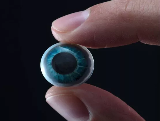
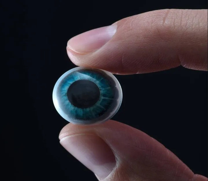
Today’s mobile devices are smaller, more power-efficient, and have more capability than we could have imagined just a decade ago. Offering ever-increasing levels of user functionality, mobile devices are now ubiquitous, and are rapidly becoming the primary mechanisms through which we interact with the digital world, our physical environment, and one another. An unintended side effect of our dependence on the current crop of mobile devices is that they are driving us to distraction.A major industry dynamic will shake things up for the better. Sensors are getting smaller and more efficient, and they’re offering attractive new functionality, giving us the ability to monitor our air and water quality, assess potential toxins in our food sources, and analyze personal health conditions, to name a few use cases. At the same time, the realization of flexible hybrid electronics (FHE) through new materials and production processes, better integration with other electronic components, more efficient energy production and consumption, and pervasive wireless connectivity are fueling the next generation of devices and experiences. What can we expect from tomorrow’s mobile devices — and how can we manage them, instead of having them manage us?SEMI’s Nishita Rao caught up with Mike Wiemer, Ph.D., VP of Engineering, CTO and co-founder, Mojo Vision, to preview his February 25 keynote, The Art of the Possible, at FLEX|MEMS Sensors Technical Congress (MSTC) 2020, February 24-27 at the DoubleTree by Hilton in San Jose, California.Join us at FLEX|MSTC to meet Mike and other industry influencers advancing innovation in FHE and MEMS sensors. Register now to connect with him at FLEX|MSTC or visit him on LinkedIn.SEMI: Mojo Vision has conducted its own research on human interaction with mobile devices. Why is this important?Wiemer: Our mobile devices have given us access to the information we need and want, improving many aspects of our lives. But our devices have also influenced our relationships and attention to our environment in negative ways. We believe that the next mobile computing platform must improve this situation. Instead of pulling us away from the moment, our devices need to embrace more human-centric engagement while still letting us access information that improves our quality of life. Mojo Vision has worked to understand this problem through our own studies and research so we can better develop an approach to address it. SEMI: How are key technical trends driving size, efficiency and capability advancements in mobile devices?Wiemer: Tiny low-power sensors are enabling ever-smaller feature-rich mobile devices that run longer on a battery charge. Smartwatches are a good example. Just a few years ago, smartwatches were not that much more than small screens on our wrists. Today, we have GPS, EKG/health monitoring, and cellular wireless interfaces all inside the same form factor.As this trend continues, we at Mojo Vision predict that our devices will continue to shrink and become even more personal: They’ll be more continuously worn and matched to our own needs and behaviors. This trend towards invisible personal devices is something we’re trying to accomplish with our solutions at Mojo Vision.SEMI: What is Mojo Vision’s concept of “Invisible Computing?” Wiemer: Our vision of Invisible Computing is based on the idea that our wearable devices should be invisible to those around us, encouraging more human interactions. These wearables should be invisible and unobtrusive to users themselves. Our Mojo Lens, which contains a full display and sensors housed inside a contact lens platform, exemplifies this vision. Using proprietary microelectronics and the world’s densest microdisplay to layer digital images and information seamlessly, Mojo Lens is redefining augmented reality. Our mobile devices today continue to increase the quantity and magnitude of interruptions. We think that shouldn’t happen. As a socially invisible device that delivers contextual, relevant content, the Mojo Lens lets us go about our daily lives, naturally interacting with other people while simultaneously enjoying the benefits of augmented reality. We think Invisible Computing can change our relationship with our devices, as well as seemingly give us superpowers. For more information, download the Mojo Vision report, Device Distraction: Understanding the Problem, Re-Thinking the Solution.SEMI: Can you tell us more about Mojo Lens?Wiemer: At its foundation, Mojo Lens is a nanoLED display, radio and sensor platform, integrated using flex technologies, and placed on your eye to provide important information. Mojo Lens can elevate or suppress this information to decrease reliance on your other devices.Unlike your smartwatch or smartphone, which react to you in a binary manner because they don’t have enough information to make autonomous decisions, Mojo Lens understands the context of your experience. That’s because it’s based on our Invisible Computing platform, which can understand your activity. Mojo Lens recognizes if you’re engaged in a conversation, driving or having a coffee, and it reacts with information accordingly.Mojo Lens could act like a real-time interpreter, for example. When someone speaks to me in a language I don’t understand, I should see “subtitles.” Or if I’m having a conversation with someone, Mojo Lens wouldn’t interrupt me with a notification at that moment. For the 92% of Americans who are interrupted by their devices during conversations every day, this prioritization can boost productivity. More importantly, it can improve the quality of our connections with the people around us.Mojo Vision’s microLED platform offers a world-record pixel pitch of over 14,000ppi and pixel density of over 200Mppi², making it the smallest, densest display for dynamic — or moving — content. SEMI: What would you like FLEX|MSTC attendees to take away from your presentation?Wiemer: It feels like the speed at which people are defining important problems and tackling them is increasing every year. And there are so many important problems to solve: space travel, autonomous driving, electric vehicles, alternative energy, quantum computing, lifespan extension, increased food production, brain-computer interfaces, AR/VR. All these problems seem impossible and “crazy,” until some group of people comes along to put a framework in place that can address them. Interestingly, these frameworks aren’t necessarily new. Rather, they build upon existing technologies and capabilities.MEMS sensors and FHE are good examples. From smart textiles, flexible displays and biological sensors to miniature radars, MEMS sensors and FHE technologies are essential building blocks. Many of the big problems we can imagine today will be solved by stacking today’s MEMs and FHE technologies in imaginative new ways. So what do we do next? I’d like to encourage FLEX|MSTC attendees to first define the problem to solve and then define the technology — rather than starting with the technology solution. Mike Weimer is a serial entrepreneur and proven science and technology leader in complex systems development and integration. Before co-founding Mojo Vision as CTO, Weimer co-founded and served as president at Solar Junction, a high-efficiency solar cell company (acquired) where he and his team set two world records for the highest-efficiency solar cells ever made by humans.After Solar Junction, Wiemer joined New Enterprise Associates (NEA) as an Entrepreneur in Residence where he sourced new investments and helped portfolio companies to develop their business and funding strategies. He is a board director at Stratio Corporation and an advisor at Stanford’s StartX Accelerator. He holds a B.S., M.S., and Ph.D. in Electrical Engineering from Stanford University.For more information, visit Mojo Vision.Interested in engaging with the MEMS sensors supply chain? MEMS Sensors Industry Group is a SEMI technology community that enables professionals in the MEMS and sensors industry to accelerate business results by addressing common challenges and opportunities.Nishita Rao is marketing manager for technology communities at SEMI.
Read More
Digitimes Research is predicting a doubling of the global SOI market between 2019 and 2024, "...thanks to significant expansion in applications to mobile devices, communication infrastructure, IoT devices and automotive electronics in the 5G era...". (Read the full article in Digitimes here.) Beyond the continued enormous success of SOI in front-end modules (FEMs) for RF (aka RF-SOI, which as we know is found in every smartphone on the planet), the report cites high growth specialty areas such as imaging chips for smartphones and photonics in data centers. They also predict that FD-SOI will be "massively applied" in 5G, with applications in base stations and data centers. And of course, low voltage and low power consumption will be the big drivers in IoT and wearables. All this is driving Soitec, the major SOI wafer manufacturer, to expand capacity at its facilities in France and Singapore in 2020, says the report. This is happening in strategic cooperation with Shanghai-based Simgui. As noted in ASN about a year ago, Soitec and China’s SOI wafer leader Simgui announced an enhanced partnership and increased production capacity of 200mm SOI wafers in China, securing future growth. At that time the two companies redefined their manufacturing and licensing relationship to better serve the growing global market for RF-SOI in mobile and Power-SOI in automotive and consumer electronics. Separately, Okmetic of Finland, which specializes in SOI wafers for MEMS, sensors and RF, is also doubling its capacity (we covered their 2019 Shanghai presentation here.) (Image courtesy: Soitec)
Read More
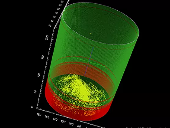
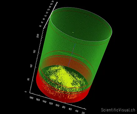
Sapphire is a precious gemstone, consisting of aluminum oxide (α-Al2O3) with occasional traces of other elements such as iron, titanium, chromium, vanadium or magnesium. While sapphire stones found in nature mostly go to jewelry applications, the lab-grown sapphire – produced in a scale of up to several hundred tons per year – is widely used by the electronic industry. Now one can hardly find a branch of technology where this crystal is not used.Sapphires are mainly applied in infrared optical components, high-durability windows, wristwatch crystals, and the very thin electronic wafers used as the insulating substrates of solid-state electronics. High thermal conductivity, low reactivity, and appropriate unit cell size make sapphire an ideal material for a wide range of such electronic substrates for manufacturing of components such as LEDs and CMOS chips.SEMI spoke with Ivan Orlov, CEO of Scientific Visual, after his presentation at SEMI Strategic Materials Conference at SEMICON Europa, 12-15 November, 2019 in Munich, Germany, to learn more about the future of sapphire.SEMI: Why is sapphire an ideal material for a wide range of electronic substrates? Orlov: Sapphire undoubted advantages are its chemical inertness and ability to withstand high temperature, radiation and mechanical loads. In addition, it exhibits low dielectric loss and very good electrical insulation that makes sapphire a good candidate for substrates for LEDs and laser diodes or wafers for epitaxial growth. However, the most important advantage is that sapphire crystal lattice does very well matching semiconductor materials deposited to its surface, in particular nitrides of group III elements. To plainly benefit from these features, the grown sapphire must have as few macro- and micro-defects as possible, as substrate defects are inherited by semiconductors layers grown on the substrate surface. Hence the importance to detect defects in the raw sapphire material. This is the area where our team at Scientific Visual contributes. SEMI: Flaws are usually identified only after costly wafering and polishing steps, because rough surface of raw crystals prevents detection of the defects. What can be done to prevent defects?Orlov: Today, major players are investing in growing larger crystals without mastering in depth the growth process. Let’s face it, the semiconductor substrate industry, which is primarily based in Asia, is using empirical research methods. The raw sapphire boules are still inspected manually, and this qualitative assessment is exploited in two folds. The first step is to further process the boule. Furnace operators then adjust the growing parameters depending on the results of the manual inspection.Due to the lack of visibility into internal crystal defects, the crystal growth and its downstream processing remain an art rather than a science. The primary reasons are the difficulty to measure, locate and quantify precisely the defects in the full crystal volume. Scientific Visual equipment enables defects in raw boules to be fully quantified and categorized. With such objective measurements and knowing the full set of growth parameters, the Process Engineering (PE) team can, with the assistance of deep learning algorithms, considerably improve the growing process. Our quality control tools give Process Engineering team the “eyes” to see complete defect distribution in raw crystals, enabling it to make minor modifications in the growth process to improve yields, reduce costs and shorten the time to market for products.SEMI: What lead to those advancements and what problems did your team set out to solve? Orlov: Breakthroughs in immersion tomography, machine vision and parallel computing drove advancements in automated quality control technology. Previously crystal inspection accuracy was limited by the acuity of the operator’s eye and subjective bias. Light distortion and the diffusion of crystals made it impossible to accurately identify internal defects.Scientific Visual equipment give operators an undistorted 3D view of all defects in a crystal boule or ingot. However, only deep learning technology can correlate a hundred thousand growth data points to identify a final defect pattern.Defect pattern in non-processed item cored from EFG sapphire plate. Well visible is a typical wavy pattern of surface layers and sandwich structure in the volume. Color code marks sapphire defect density: from deep blue (non-defective material) to deep red (highest defectiveness.) SEMI: What challenges are addressed by your approach? Orlov: Increasing the yield of semiconductor substrates like Sapphire, Gallium Nitride and Silicon Carbide is paramount to reducing the price of wafers while increasing their quality. The upstream growth and downstream wafering processes are not deterministic. So far, most of the producers can only determine the quality during the late stages of the process. This condition creates huge constraints for teams in charge of production and processing. Automated Quality Control (QC) at the early stage of the production chain relieves all the unknowns, ultimately reduce the cost of material.SEMI: And what are the main opportunities?Orlov: There are massive opportunities to increase the yield and to ease the full processing chain from growth to the wafering process. Objective Quality Control (OQC) paves the way to industry-wide standards that categorize crystal quality at each step of growth to enable full certification of the defectiveness of the material and facilitate its trade and exchange.SEMI: What’s one of your predictions for the future of new materials?Orlov: The explosion of e-mobility and electric vehicles and the development of other green technologies will drive rising demand for low-defect sapphire, silicon carbide and gallium nitride substrates thanks to the streamlining of the full processing chain. Manual quality control will soon give way to full automation as quality control in sapphire and other raw crystals production is the only missing link in a fully automated semiconductor production chain. I believe that in five years, automated raw crystal inspection will become standard in the industry. Our mission is to empower every crystal grower to achieve this important milestone.Dr. Ivan Orlov obtained a Ph.D. in Crystallography from the Federal University of Technology in Switzerland EPFL and an MSc in Solid-State Physics in Moscow, Russia. Ivan co-founded Scientific Visual in 2010 to answer the challenge of the synthetic crystals industry struggling with high defect yield. Prior to this he worked in a company specialized in diamond optics. He has more than 10 years of experience in R D with focus on optical materials, industrial crystals and non-destructive quality control technologies. Dr. Orlov was a SEMI Task Force member for sapphire standard development in China and collaborates with ISO committee in Switzerland to establish industry-wide sapphire quality standards.Serena Brischetto is senior marketing and communications manager at SEMI Europe.
Read More
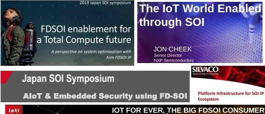
Here is our second post about the SOI Consortium’s Japan Symposium this past fall. This will provide summaries of eight very informative presentations on SOI in IoT and automotive by NXP, Dolphin Design, Leti, Silvaco, Arm, I-fuse and Secure-IC. There’s a lot of content to summarize, so this post is about twice as long as those we usually do. But you’ll want to read right to the end, for sure! In case you missed our previous post on the 5G/RF-SOI presentations given at the Japan event, you can read it here. Our next and final post on the Japan event will cover photonics presentations by Cisco/Luxtera, TowerJazz, GlobalFoundries, Leti, Cadence and Soitec. By way of reminder, the Japan SOI Symposium was a great success, with both days well attended. If your company is a member of the SOI Consortium, you can now access most of these presentations on our website. You can also click on the illustrations in this post to see them in enlarged versions. [caption id="attachment_28106" align="alignleft" width="366"] (Courtesy: NXP SOI Consortium)[/caption] The IoT World Enabled Through SOI - Jon Cheek, NXP Sr. Director, Front-End Innovation For NXP, FD-SOI introduced the ability to easily add different functionalities to the technology node like ULP, eNVM, support for high-voltage and embedding RF. For them, said Cheek, it’s about the range, and with adaptive back bias, you can “get crazy”, so you can really achieve amazing things. In fact, they think they now have the lowest leakage SRAM in the industry, thanks to body biasing. The i.MX 7ULP is finding significant success in wearables. Their “crossover” chips are the latest beneficiaries of FD-SOI with body biasing. The “new normal”, they offer huge improvements for real-time operating systems – which is of course key for edge computing. (As you can imagine, the audience was intently taking notes throughout -- this was a really excellent talk!) It also is great for machine learning, as it is designed to unlock the potential of voice-assisted end nodes. The IP they needed is now available from multiple vendors, noted Cheek, such as Tensilica and VeriSilicon. Another key play will be in visuals for industrial computing. He concluded by observing that the automobile is the ultimate IoT machine, with 10x the amount of code now found in leading edge airplanes. That’s where the i.MX8 and 8X come in. [caption id="attachment_28104" align="alignright" width="323"] (Courtesy: NXP SOI Consortium)[/caption] High-Voltage SOI – Enabling Automotive- NXP Jon Cheek gave this presentation on the second day of the Japan event. Long-time followers of SOI will know that NXP has been excelling in high-voltage (HV) SOI for well over two decades now (including the pioneering work done by Philips, now part of NXP: their EZ-HV SOI patent dates back to 1993). It’s probably safe to say that NXP's SOI-based automotive chips are used by virtually every carmaker on the planet. HV follows well behind the leading edge – it’s currently mostly around 130nm (the limits are related to metalization). Reason #1 it’s on SOI? SOI-based technologies are incredibly reliable, especially in the automotive culture targeting the three zeros (0 emissions, 0 accidents and 0 time wasted). Today’s car manufacturer’s are going to a distributed environment, and SOI still provides a huge advantage, making parts that are smaller, lower power and more reliable – so it drives a lower BOM for automakers.In conclusion, said Cheek, NXP’s leadership through SOI innovation enables scalable solutions, high voltage analog integration, sensor integration, and reliable safe passenger experience. [caption id="attachment_28101" align="alignleft" width="432"] (Courtesy: Dolphin Design SOI Consortium)[/caption] Improving SoC Energy-Efficiency with Dolphin Design Platforms – Nicolaus Gaude, BizDev Product Marketing, Dolphin Design Dolphin has a series of platforms, techniques and IP for increasing speed and drastically improving energy efficiency in SoC design. Gaude introduced their Speed Platforms, which include a Power Management Platform and a Processing platform, both of which make dramatic improvements in energy efficiency. The Power Management Platform keeps control of power management from architecture to design, resulting in a 10x improvement in energy efficiency. The Processing Platform comprises configurable RTL clusters for best-in-class (100x) energy-efficiency. Gaude then turned to the Dolphin’s Adaptive-Body Bias (ABB) IP for breakthrough energy-efficiency with FD-SOI. This is real-time, “on-the-fly” body biasing: the IP does it all. It is silicon-proven on GlobalFoundries’ 22FDX with Arm cores and Invecus standards cells SRAM, with breakthrough energy efficiency. [caption id="attachment_28108" align="alignright" width="363"] (Courtesy: Silvaco SOI Consortium)[/caption] Platform Infrastructure for SOI-IP Ecosystem – Thomas Blaesi, VP of Global Marketing, Silvaco The massive use of IP is both an advantage and a challenge, began Blaesi. There are solutions out there, but they are disconnected. Typically SoC/IP designers, IP librarians and support folks use various systems, while procurement, finance and legal use others. This is a problem for both the providers and the consumers of IP. Silvaco has a new system called Xena that centrally organizes all IP data: it’s an IP repository for tracking accounts, products, contracts, devices, support, compliance and reporting. One of the first beneficiaries of Xena will be the SOI ecosystem, as providers of SOI IP are already signing on. Beyond the organizational advantages, Xena has patented “finger printing” and “DNA analysis”, so there is a digital representation of each IP on an SoC that can’t be reverse engineered. Each fingerprint contains list of unique signatures of each file in an IP or SoC. A file’s unique signature is created from the entire file content, and that signature is guaranteed to be unique to that content. It enhances support for all versions of common design files: hard IP, soft IP, and embedded software. Because it’s cloud or enterprise based, it will be particularly useful for large organizations. Fingerprinting and DNA analysis are vendor agnostic, universal, and easy-to-use tools and methodologies for IP lifecycle management, he concluded. [caption id="attachment_28103" align="alignleft" width="463"] (Courtesy: Leti SOI Consortium)[/caption] Ultra-low power, FD-SOI based IP, in the space of IoT, Health Care, Smart Connectivity 5G – Michael Tchagaspanian, EVP Industrial Partnerships, CEA-Leti This presentation began with a review of the explosion in devices with IoT and related investments, then connected all the ways in which innovations powerhouse Leti is contributing – from the SOI wafer level to the chip level – which is to say practically everywhere! Especially hot topics in FD-SOI included: the roadmap to sub-10nm; CoolCube monolithic 3D; new embedded memories; power amplifiers; Ultra-Wide Range DSP; smart sensing local processing (including haptics, imaging, infrared advanced processing); local processing with edge AI; and spike coding for deep neural networks. He showed information on two always-on/on-demand transmission 28nm FD-SOI IoT test chips that taped out in mid-2019: the Warrior and the Samurai. And finally, he covered silicon-proven IP that Leti has for FD-SOI including power management blocks, lots of RF IP (including low-power RF wake-up), sensor interfaces, clockless network-on-chip and new SRAM technologies. These and more will be covered at the next Leti Innovation Days in Grenoble (June 2020) – during which in parallel, btw, there will also be a European SOI Summit hosted by the SOI Consortium. [caption id="attachment_28099" align="alignright" width="475"] (Courtesy: Arm SOI Consortium)[/caption] FDSOI Enablement for a Total Compute Future – Manuj Rahor, Director Emerging Technologies Product Marketing, Arm Subtitled A perspective on system optimization with Arm FDSOI IP, this presentation reviewed how Arm is enabling system gains through optimization across IP boundaries. This is work happening in the Arm Artisan Physical Design Group (PDG), which provides logic, memory and POP (processor optimization package) IP as well as various products to help ease implementation challenges for advanced nodes. In this case the focus is on Total Compute enablers on Samsung 28nm FD-SOI (called 28FDS) – specifically three building blocks recently launched on FD-SOI. The first is the 128Mb Wide Capacity embedded MRAM (an eNVM to replace eFlash) compiler for storage delivered to Samsung in July `19. It was demonstrated in silicon in the Musca-S1 Smart IoT Device Demonstrator on 28FDS, an energy efficient IoT device with eMRAM secure boot on-chip storage. [Read our coverage from March 2019 here.] The second is a novel design developed with Spin Memory. It recently taped out on 28FDS and is slated for delivery in 2020. Adding an “Endurance Engine to the eMRAM that was delivered in 2019, the ARM-Spin innovation delivers RAM-like performance with increased speed and endurance. What’s at issue here is a change in use cases. Use cases served by eFlash were not written to that often; now with sensors (as in IoT) that continually gather and write data, eFlash endurance is not sufficient. The third is billed as an SRAM replacement compiler. Its MRAM as RAM in A-class systems, with significant energy and performance gains. Again, this is a use-case issue: retention is lower (this is for weeks months, whereas the other solutions are for 10 years). But you can get more RAM than SRAM into the same footprint, so you get a 60% reduction in DRAM traffic and increased performance. Delivery for this is marked as 2020+. [caption id="attachment_28100" align="alignleft" width="294"] (Courtesy: Attopsemi SOI Consortium)[/caption] I-fuse™: A Disruptive OTP Technology – Dr. Shine Chung, Chairman, Attopsemi I-fuse is a disruptive OTP (One-Time Programmable) technology without disrupting a fuse. The goal was a 100x increase in reliability at 1/100th of the cell size and 1/10th the power. It has now been demonstrated in GlobalFoundries’ 22FDX FD-SOI technology for energy harvesting applications. In the OTP IP technologies, explained Dr. Chung, they defied the conventional wisdom of breaking a fuse to maintain a permanent programmed state forever: Attopsemi’s I-fuse™ is actually a “non-breaking” fuse. “I don’t mind to break a fuse, but I do care about breaking a fuse by explosion”, said Dr. Chung. “The I-V curve of programming a fuse beyond the break point actually shows more like an explosion. The anti-fuse OTP also ruptures gate oxide by explosion. On the contrary, I-fuse™ is a disruptive OTP technology without disrupting a fuse.” He concluded, “By using MOS as switches to enable discharging two capacitors, through cell and reference cell respectively, and compare the discharge rates, the resistance in the cell can be determined higher or lower than the reference resistance so as to convert into logic data. The read energy consumed is only 1/100 of the conventional sensing, which is good for energy harvest IoT applications. Eventually most IoT devices will be battery-less.” [caption id="attachment_28107" align="alignright" width="398"] (Courtesy: Secure-IC SOI Consortium)[/caption] AIoT Embedded Security Using FD-SOI – Yan-Taro Clochard, Japan Sales Director, Secure-IC In addition to opportunities, the impact of AI on IoT (aka AIoT) adds new threats to edge devices. Design for security and in-depth security is required, down to the physical layer. For example in automotive, sensors gather data and AI analyzes it – but the enabler is security. The challenge of AI is the increase in data and connectivity with unsecured devices. FD-SOI is a key for Secure-IC’s Securyzer security module: it leveragesFD-SOI properties to secure the AIoT world. It is flexible, and tuned for each customer. Here, FD-SOI enables the creation of physically secure systems, with secure boot and firmware updates, cryptographic services, key management and secure storage.

Read More
In a shining hour for Prof. Mike Czerniak, environmental manager for Edwards Ltd., a SEMI member company, and Chemistry Prof. Simon O’ Doherty of the University of Bristol, the educators presented a case study on efforts by the semiconductor and aluminum industries to mitigate greenhouse gas emissions – part of an online Bristol Futures course that won the National Award in the Next Generation Learning and Skills category of the prestigious Green Gown Awards.The online students hailed the semiconductor industry as an exemplar of applying abatement systems to the reduction of greenhouse gas emissions as well as an excellent example of an engaged industry and true dedication to sustainable development. The course – Unleash Your Potential: Sustainable Futures – encourages students to learn about the sustainability challenges of the modern world and make a positive contribution to society.This four-week online course takes learners on a journey to explore their personal views and understanding of sustainable development, then addresses challenges faced by the city of Bristol and globally before bringing them back to the personal. The case study features academics and industrial partners discussing the challenges of greenhouse gas emissions and the benefits of cutting-edge collaborations aimed at driving long-term solutions.Hosted on the FutureLearn platform and offered three times a year, the free online course is structured around the United Nations Sustainable Development Goals (SDGs) to provide fascinating, solution-based narratives in the era of the Anthropocene.The University of Bristol launched Bristol Futures in 2018 and the initiative centers on three themes: Global Citizenship, Sustainable Futures and Innovation, and Enterprise. The interdisciplinary team that developed the Sustainable Futures theme consisted of myself (Ph.D. candidate, Chemistry/Geography), Chris Preist (Professor, Computer Science and Sustainability) and Aisling Tierney (Ph.D. Archeology); this interdisciplinary approach was introduced by sustainable development pioneers Chris Willmore (Professor of Law and Sustainability) and Martin Wiles (Head of Sustainability)The case studies have one particular strength – a sweeping diversity of contributors to reflect the endless possibilities of sustainable development. The 10-minute videos engage learners with academics, researchers, industrial experts, students, government and non-government organizations and communities. The Head of Unesco for Maritime Affairs, goat herders in Croatia, authors, the Intergovernmental Panel on Climate Change (IPCC), first-year university students – they all add their special flavor to sustainable development.Established in 2004, the Green Gown Awards recognize the exceptional sustainability initiatives being undertaken by universities and colleges. We are extremely proud that this online course has been recognized as sector leading by the Green Gown Awards and thrilled that the Sustainable Futures online course has been taken by more than 5,700 people, including over 2,000 students at the University of Bristol.We hope that the Sustainable Futures family will continue to grow and invite you to join us in this exploration of sustainable development, global challenges and yourself in our next run starting in February 2020!Eleni Michalopoulou is a Ph.D. candidate, Atmospheric Chemistry Research Group, School of Chemistry, at the University of Bristol.
Read More