downloadGroupGroupnoun_press release_995423_000000 copyGroupnoun_Feed_96767_000000Group 19noun_pictures_1817522_000000Member company iconResource item iconStore item iconGroup 19Group 19noun_Photo_2085192_000000 Copynoun_presentation_2096081_000000Group 19Group Copy 7noun_webinar_692730_000000Path
Skip to main content
Default Banner Image

Technology and Trends

In the first part of this double feature, we looked at the automotive industry’s transition toward a mobility ecosystem and the shifting business model perspective from selling vehicles to miles. At the core of these changing dynamics are four trends represented by the acronym ACES: Autonomous, Connected, Electric, and Shared mobility. Each of these trends is largely enabled by microelectronics through computer processors, sensor units, and communication architectures. Part 2 of this series explores the business opportunities at the transition from automotive to mobility, and the specific role SEMI can play as a natural bridge between the two ecosystems.Electronics and Software as Drivers for Automotive InnovationThe ACES trends represent an acceleration of the shift in automotive from the industry’s traditionally strong focus on mechanics and hardware toward electronics and software. This transition to electronics and software as drivers for automotive innovation already started in the 1970s with electronic fuel injection, anti-lock brakes, trip computers, and many other attributes that are now considered standard features. As a result, there are now hardly any automotive systems that are not computer-controlled. A vehicle without power windows and locks, electronic climate control, or MEMS-reliant airbags are basically unimaginable in many markets.As shown in the graphic[1] depicting the electronics share of total vehicle cost, the numbers paint a clear picture of the continued growth of electronics over time, with a 44% share today expected to grow to 50% by 2030. McKinsey Company estimates the automotive software and electrical/electronic (E/E) components markets combined will grow at a 7% CAGR from USD 238 billion in 2020 to US$469 billion by 2030[2].The assumption of continued and sustained growth presents a promising outlook for semiconductor and sensor content in vehicles over the next decade, which is particularly strong in the electrification space. Hybrid electric vehicles (HEVs) already contain $900 worth of semiconductor content, and battery-based electric vehicles (EVs) contain $1,000 worth of semiconductors – much higher than the average of approximately $450 of content in conventional vehicles[2]. Other business opportunities in the mid-term (3-5 years) include software, battery technology, infrastructure (charging stations, other hardware components, etc.), as well as vehicle-to-vehicle (V2V) and vehicle-to-environment (V2X) communication. These technologies also demonstrate how the industry’s business focus is expanding beyond the confinement of an individual vehicle to increasingly contemplating the evolving ecosystem around it, resulting in real mobility solutions. Image credit: Continental AG This creates significant opportunities for a large number of SEMI members in the semiconductors and sensors business by connecting them with new customers and partners in the automotive and mobility supply chains, primarily vehicle manufacturers and Tier 1 suppliers, and together realizing new business in new automotive applications such as: Autonomy, including ADAS (GPUs, LiDAR, radar, camera, accelerometers...) Connectivity (link to outside infrastructure and in-cabin devices, roadside units...) Electrification (power electronics, battery monitoring, H2 detection in fuel-cell...) Sharing (customizable vehicle interior, trackable mobility devices such as scooters...) In-cabin experience (media systems, displays, VR/AR, occupant detection...) Vehicle architecture (flex-ray, automotive ethernet, diagnostics, smart parts...) Safety and security (HW/SW firewall, parts authentication, upgradability...) In these partnerships, the vehicle manufacturers and component suppliers clearly benefit from leveraging semiconductor capabilities including: Device and system reliability/robustness/quality (“Zero Defect”), which creates opportunities for new SEMI Standards (e.g. wafer-to-device/system traceability) New design architectures for added functionality, safety and security New packaging solutions (automotive OEMs are already participating in the Heterogeneous Integration Roadmap, seeking to collaborate with device manufactures and Original Semiconductor Assembly Test (OSAT) companies to reduce costs and differentiate on automotive-grade solutions Sensors and imaging (cameras) SEMI Smart Mobility Initiative – Connecting Mobility and ElectronicsSEMI launched its Smart Mobility Initiative in 2018 based on the mandate of providing “SEMI members with access to new business opportunities and collaborative platforms in the automotive electronics supply chain.” The initiative is currently focused on synchronizing the automotive and microelectronics supply chains for automotive electronics innovation – in particular semiconductor devices, sensors, and related products manufactured for this space and sold to vehicle OEMs and Tier 1s. To facilitate closer dialogue among stakeholders from this combined ecosystem, SEMI formed the Global Automotive Advisory Council (GAAC) which now has five regional chapters and represents dozens of companies. Collectively, GAAC members discuss and act on a wide range of topics, from Silicon Carbide (SiC) standardization to new design architectures and closing the OEM requirement gap.While continuing to build on the strong automotive foundation, SEMI’s Smart Mobility Initiative is now expanding its reach and scope of activities to broader mobility themes, such as infrastructure and battery technology and Smart City, to infuse SEMI member communities and the GAAC with new stakeholders and new ideas. These are exciting times!Please contact Bettina Weiss, Chief of Staff at SEMI, at [email protected] for further information about SEMI’s Smart Mobility Initiative, the Global Automotive Advisory Council, and how SEMI can help your organization navigate electronics in the automotive industry to drive innovation in the mobility space.[1] see graphic, created with data from NXP / Freescale[2] Source: McKinsey Company, 2019Microelectronics Power the Future of Mobility – Part 1: Autonomous, Connected, Electric and SharedBettina Weiss is Chief of Staff and Global Smart Mobility Lead at SEMI. Sven Beiker is Smart Mobility Consultant at SEMI.
Read More
While the full contours of the next normal are still unclear, semiconductor companies largely acted decisively at the beginning of the crisis to build resilience and position the sector for future growth. To plan ahead, now is the time to think about the next normal and set the strategic direction needed to emerge even stronger from this humanitarian and economic crisis.Global GDP recoveryMcKinsey has developed nine GDP recovery scenarios, and as the economic situation has developed, we surveyed more than 2,000 global executives to discover that two of those scenarios are most likely. Both of those scenarios assume that the spread of coronavirus is eventually controlled and catastrophic economic damage is avoided. In the first scenario, global GDP is expected to recover in the first quarter of 2021; in the second, recovery is forecasted to be delayed until late 2022. The geographies of recovery will vary, as some industries and regions will recover faster than others.Semiconductor Demand Forecast for 2020 and 2021The COVID-19 crisis has created an unprecedented challenge for the semiconductor industry. During the 2007/2008 recession, consumer demand stagnated. This crisis, however, has affected both demand and supply, creating dual pressures. Our demand forecast is based on the two most likely McKinsey GDP recovery scenarios as well as on extensive surveys, expert interviews and research on the recovery in China. Charts 1 and 2 (below) show that the semiconductor market as a whole is expected to decline by up to 10% in 2020 due to the COVID-19 outbreak and the resulting slowdown in the global economy. In 2021, however, most segments are expected to grow, with total market size surpassing 2019 value in the more positive scenario. The PC market segments will see the least growth, while the wireless communication and automotive segments should expect to be hit hardest by this crisis with a decline of as much as 21% and 27% respectively in 2020. However, they are expected to bounce back in 2021 with growth of up to 19% and 36% in the positive outlook scenario.It might take some time for the semiconductor market to fully recover. The timing of the industry’s recovery depends largely on the containment of the virus, government economic stabilization efforts, and the global economic recovery.1. Products include memory, micro components, logic, analog, discrete, optoelectronics, and sensors/actuators.2. 2020 estimates were calculated using 2019 baseline and percentages have been rounded.3. Gray values indicate 2020 growth forecast; blue values indicate growth forecast for 2021 only. Sources: IHS, Expert Interviews 1. Products include memory, micro components, logic, analog, discrete, optoelectronics, and sensors/actuators.2. 2020 estimates were calculated using 2019 baseline and percentages have been rounded.3. Gray values indicate 2020 growth forecast; blue values indicate growth forecast for 2021 only.Sources: IHS, Expert Interviews Emerging stronger from this crisisSemiconductor companies had already developed effective crisis-management strategies during past crisis and industry downturns. However, this situation is unique. Overall, we see three main activities that can help semiconductor players with through-cycle resilience and growth: Define the starting position: Creating a baseline can help inform future strategic decisions by providing a holistic view of the current strategy, internal capabilities and external position. Develop economic and political recovery scenarios: Developing and deciding which economic and political recovery scenarios to focus on will enable companies to create company specific scenarios. Therefore, it is important to analyze demand in the short and long terms, along with the effects of subsidies, stimulus packages and industry dynamics. Prepare for the next normal: To prepare for the next normal and emerge even stronger from this crisis, companies should focus on how to gain market share during the downturn. As competitors focus on resilience, companies who see themselves in a financially stable position can focus on increasing their company’s growth and market share. This mindset, however, is most effective when established across the entire organization. Opportunities to emerge even stronger include defining a strategic, systematic approach to investment and divestment as appropriate. This means that several smaller deals that accrue to a meaningful amount of market capitalization over the years often have a more positive impact than one large transaction. History tells us that finding pockets of growth and revising capex, R D and M A strategies are the building block to emerge stronger from a crisis. As Gordon Moore, co-founder of Intel once said, "You can't save your way out of a recession." This translates into moderate capex and R D budget cuts with the focus on future growth drivers. These approaches are supported by insights from previous crises.Although the crisis has presented a major challenge, it also offers the chance for companies to set themselves apart from competitors. The semiconductor industry as a whole has been more resilient than many other industries. The global push toward digitization has also been a major tailwind that will likely be a key element of the global economic recovery.Ondrej Burkacky is a partner with McKinsey Company based in its Munich office. He leads McKinsey’s semiconductor and software work in Europe, as well as its global COVID-19 semiconductor task force. For McKinsey’s latest insights on the business implications of the coronavirus pandemic, visit its website, which is updated daily.
Read More
As the amount of electronics in automobiles continues to increase, it is becoming more common to hear a vehicle referred to as a “computer on wheels.” To that end, innovation occurs at the intersection of automotive and microelectronics so that leveraging synergies and contemplating joint initiatives becomes crucial in shaping the future of both fields. In this two-part article, we will discuss the current trends in the automotive industry, which are to a large extent driven by microelectronics, and will reflect on the transition from “just the vehicle” to “the mobility ecosystem.”SEMI encourages its members to partner in seizing opportunities in safe, efficient, and convenient mobility solutions. Before diving into specific opportunities that the automotive industry offers to electronics companies, we will start by taking a closer look at this sector and the current trends.Automotive or Mobility? Shaping the New EcosystemThe automotive industry and its supply chain of vehicle manufacturers and component suppliers has been evolving for decades around the sales of vehicles. The customer groups used to be fairly well established with individual consumers and commercial entities, the latter often as fleets. The automotive industry has grown in depth by vertically integrating design, manufacturing, sales, service, accessories, etc. More recently, the traditional players have also begun to venture into mobility services such as car sharing, showing their ambitions to become “mobility providers.”The term “mobility” has been used increasingly instead of “automotive” for about a decade now. This reflects the more recent transition to creating businesses and functionalities around the sales of miles. In line with this, the industry’s perspective is also shifting toward use-cases and experience rather than just focusing on the vehicle or plain transportation. Much of this transition from “vehicles to miles” is driven by key trends that require massive use of microelectronics, in particular autonomous driving and electric vehicles.One of the key questions to raise for SEMI members is: at which stages should the supply chains for the microelectronics and mobility industries interact with one another to shape the evolving ecosystem? In order to answer this question, we will examine the four main trends shaping the future of mobility represented in the acronym “ACES”: Autonomous, Connected, Electric, Shared.ACES – Autonomous, Connected, Electric, SharedThese four trends, together with the broader transition from “vehicle to miles,” also include newcomers “disrupting” the industry and changing it for good. Basically, every mobility player, traditional or new, is taking ACES (or CASE) into consideration at the moment.Autonomy: computers are taking over the task of driving from humans, first through advanced driver assistance systems (ADAS) and then at some point with complete self-driving. Following the levels of automation from zero to five, as defined by SAE International[1], the current market frontier is SAE Level 2, which means the vehicle can under certain situations (e.g. highway) drive itself but has to be monitored by the driver at all times. Many industry experts assume that artificial intelligence and computing power hold the key to higher levels of automation.Connectivity: vehicles are increasingly exchanging data with a central hub and with one another through cellular, WiFi, satellite, etc. At present, there are mostly entertainment and convenience offerings on the market, but maintenance and safety functionalities are emerging. One key differentiation between solutions is whether connectivity is “built-in” with embedded OEM solutions, “brought-in” (e.g. smartphone apps independent of vehicle or dashboard navigation systems), or “tethered” (e.g. smartphone used as communication gateway).Electrification: traditional mechanical and fossil-fuel-powered vehicle driveline components are increasingly being replaced by electrical components. The spectrum includes hybrid electric vehicles (HEV), plug-in HEV (PHEV), battery-based electric vehicles (EV), and hydrogen fuel-cell vehicles (FCV). The transition from traditional to electrified driveline technology requires more and more diverse electronics, such as more control systems, sensors and high-voltage systems. Ultimately though, the transition requires fewer systems, i.e. ignition, injection and multiple other systems being replaced by high-voltage power electronics and battery monitoring.Sharing: a growing number of consumers are seeking convenient access to mobility to get “from A to B” while viewing vehicle ownership as a burden rather than a benefit. Typical forms of this trend include car-sharing, ride-sharing, ride-hailing, micro-mobility, and micro-transit. Mobile computing enables much of the convenience that shared mobility offers, such as instant access, competitive and convenient payments, and flexible work opportunities (i.e. “gig economy”). Therefore, electronics, connectivity, and computing all play an important role in this trend.SEMI as the Natural Convener for Industry Exchange and ProgressClearly, for all four of the ACES trends, microelectronics play a crucial role in driving mobility innovation and making future solutions safe, efficient, and convenient. Based on this, mobility represents one of the largest opportunities for semiconductors: by 2025[2], a projected 14% of all integrated circuits produced globally will go into vehicles. As the trade association representing the complete microelectronics manufacturing and design supply chain, SEMI is positioned as a natural convener of experts for cross-industry and pre-competitive exchanges with the automotive supply chain. This positioning led to the foundation of the Smart Mobility initiative at SEMI, in part, to facilitate collaboration across these increasingly interdependent supply chains. The second part of this blog will present opportunities for electronics based on the ACES trends in the automotive industry, along with an overview of the Smart Mobility initiative.[1] © SAE International from SAE J3016™ Taxonomy and Definitions for Terms Related to Driving Automation Systems for On-Road Motor Vehicles (2018-06-05), https://www.sae.org/standards/content/j3016_201806/ (retrieved 05/5/2020)[2] Source: IC InsightsMicroelectronics Power the Future of Mobility – Part 2: Opportunities for ElectronicsBettina Weiss is Chief of Staff and Global Smart Mobility Lead at SEMI. Sven Beiker is Smart Mobility Consultant at SEMI.
Read More
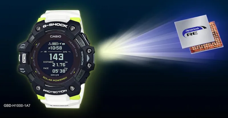
SkyWater Licenses Key FDSOI Technology From MIT Lincoln Laboratory, Moves Up Availability Of Its 90 Nm Strategic Rad-Hard By Process Offering. (press release, 11 June 2020) Transferring MIT Lincoln Laboratory’s proven 90 nm FDSOI process into SkyWater’s Trusted fab will enable accelerated delivery on a previously announced up to $170 million Department of Defense (DOD)-funded program at SkyWater to enhance microelectronics capabilities for the Department and develop a new 90 nm Strategic Rad-Hard by Process manufacturing flow.Green Hills Software Adds Support for the Heterogeneous NXP i.MX 8 Application Processors in Airborne Safety- and Security-Critical Systems (GHS press release, 19 May 2020). Per the release, “NXP i.MX 8 applications processors have several features that are useful for avionics, airborne mission computers, and cockpit displays. With four Cortex-A53 cores and two Cortex-A72 cores, the i.MX 8QuadMax enables power consumption optimization by matching the performance requirements of each application task to the performance capacities of the different cores. The low soft-error rate of i.MX 8 processors results from a robust 28 nm FDSOI manufacturing process, which has inherently high immunity to alpha particle flux and enables high MTBF. Along with many of NXP's product families, the i.MX 8 processors have a minimum of 10-15 years of product supply longevity.”IBM Power9: Digging Into the Architecture and Materials - 14 May 2020. EETimes article by Jeongdong Choe ofTechInsights. This article summarizes TechInsights' analysis of the IBM 14HP HKMG FinFET-on-SOI eDRAM cell architecture, process, and design recently used in the IBM Power9 processor, which is fabbed by GlobalFoundries. It includes a list of new GF innovations, especially in the areas of architecture, process, materials and design.A major advance in high-performance computing - Leti Press Release, 7 May 2020. ​CEA-Leti unveiled a state-of-the-art demonstrator chip for high-performance computing applications at ISSCC 2020. The low-cost, energy-efficient processor is built on an innovative multi-core system that is both modular and expandable. The 96-core demonstrator is arranged into six FDSOI chiplets 3D integrated onto the active 65 nm silicon interposer.Silicon Photonics: A Marriage of Optical and Digital on GF’s RF Process - GF's Foundry Files blog, May 07, 2020. GF and Ayar Labs collaborated on ways to optimize GF’s 45 RF SOI process for the optical structures and other functions. That technology, developed for the mmWave market, was modified to include photonic function and is now being used to build prototypes. RF SOI CMOS is an “enabling thing, because it allows us to build both transistors and optical devices in the same planar layer. And the SOI process enables extremely fast transistors, faster than most of the advanced nodes built today."Webcast interview with Maud Vinet (in French),Quantum hardware program manager at CEA-Leti - 6 May 2020. Maud Vinet was also a key driver in the research and development of FD-SOI, and was recently awarded the French Legion of Honor award.Dolphin Design Unveiling innovative Energy Efficient Platforms, complete turnkey solutions for competitive SoC designs - Dolphin Design announcement, 4 May 2020. The company is releasing 4 platforms in the coming weeks: SPEED Power Management, SPEED Processing MCU, SPEED ML/AI Processing and/or SPEED Audio.Silicon Catalyst Collaborates with Arm to Accelerate Semiconductor Startups - Silicon Catalyst press release, 29 April 2020.Arm joins as Strategic Partner and as In-Kind Partner - the first company to join the incubator in both roles. The partnership provides startups with no-cost access to a broad range of Arm® IP, tools and support.Mixel’s MIPI D-PHY IP Integrated into the Lattice CrossLink-NX FPGA - World’s first low-power FPGA to support D-PHY v1.2 with 2.5Gbps/lane. Mixel press release, 28 April 2020. The new CrossLink-NX FPGAs are built on Samsung’s 28nm FD-SOI technology.GlobalFoundries Dresden Certified to Manufacture Secure Products - GF Press release, 27 April 2020. The official BSI certification extends the ability to cost effectively manufacture secure, connected products to GlobalFoundries’ 22FDX (FD-SOI) technology.GlobalFoundries Qualifies Synopsys' IC Validator for Signoff Verification on 22FDX Platform - Synopsys press release, 16 April 2020. With IC Validator physical verification, customers striving to take advantage of the low-power and performance benefits of GF's FD-SOI technology can now quickly verify that their designs meet signoff requirements for manufacturability compliance and maximum yield. Signoff design rule check (DRC), design for manufacturability (DFM), layout vs schematic (LVS) and metal fill runsets and tech files are available today from GF.FDSOI and Migration - YouTube video by Thalia Design Automation, posted 14 April 2020. Founder/CTO Sowmyan Rajagopalan talks about why analog IP reuse is a big problem for semiconductor companies, who Thalia is and how they can help. RF SOI can Save $Billions in 5G mmWave Network Costs with Efficient PAs - cover story in Microwave Journal, 13 April 2020. Republished here in its entirety with permission. By GlobalFoundries, Mobile Experts Mixcomm. Compact Model Developed at CEA-Leti for FD-SOI Technologies Designated as a Chip-Industry Standard - Leti press release, 2 April 2020. This Is of Paramount Importance for Large Chipmakers And Positions CEA-Leti Among the Few Compact-Model Developer Teams Able to Develop and Support a Standard ModelLattice Semiconductor Joins Silicon Catalyst In-Kind Partner Ecosystem to Foster Broader Use of FPGAs - Silicon Catalyst press release, 2 April 2020.eNVM Technology Choices for Automotive, Industrial and Multi-market Solutions - Video posted April 2020 by GlobalFoundries and SemiWiki. Perceive Corporation Launches to Deliver Data Center-Class Accuracy and Performance at Ultra-Low Power for Consumer Devices - Perceive press release, 31 March 2020. Introduces breakthrough Ergo™️ edge inference processor, delivering 4+ TOPS sustainedand 55 TOPS/W, capable of processing large neural networks in 20mW. The company has partnered with the leading specialty foundry, GLOBALFOUNDRIES, to manufacture the Ergo chip on their 22FDX® platform.Photonic Solutions From Synopsys Support Advancements in Nanoscale Optics - Synopsys press release, 30 March 2020. This latest Photonic Solutions Portfolio accelerates design of AR/VR Systems, Optical Communications, and PICs. Additional details were given by Synopsys during the SOI Consortium's Japan Symposium.Casio Tips Its Hat to Renesas for Its Battery-Less, Solar-Powered Smartwatch. In All About Circuits, March 19, 2020. The GBD-H1000, a new member of Casio's G-SHOCK line of smartwatches, functions on harvested energy. It also features a heart rate monitor and GPS functionality. Casio says the new watch needs no battery since it can be completely solar powered. Casio Computer Co. chose the Renesas RE01 controller as the primary controller. Renesas’ RE01 Group products are extremely low-power devices based on SOTB (what Renesas calls their flavor of FD-SOI) process technology. (Note that Casio has been using FD-SOI based chips in their G-Shock watches since 2005.)Bluetooth IP migration and leveraging FDSOI back gate biasing feature - Thalia Design Automation blog, 16 March 2020. By Founder/CTO Sowmyan Rajagopalan. QuickLogic's eFPGA Qualified on GLOBALFOUNDRIES 22FDX® Platform for IoT and Edge AI Applications - QuickLogic press release, 11 March 2020.D R FDSOI IP SoC Day - Virtual IP Event - hosted by Design Reuse, 13 March 2020. View videos get presentations by SOI Consortium members ST, Soitec, Analog Bits, Dolphin Design, Leti and Thalia, as well as other industry experts.Analog FD-SOI : Body biasing techniques enable designers to trade speed and power - Thalia Design Automation blog, 9 March 2020. By Founder/CTO Sowmyan Rajagopalan. Soitec's engineered substrates for 5G - Soitec (press release, 4 March 2020)Working with GF: Why MixComm Chose GF's Industry Leading 45RFSOI Solution - GlobalFoundries, YouTube video posted 18 March 2020. TCAD Simulations of RF-SOI Switches with Trap-Rich Substrate - Silvaco, by Graham Bell, 2 March 2020. GlobalFoundries Delivers Industry’s First Production-ready eMRAM on 22FDX Platform for IoT and Automotive Applications - GlobalFoundries (press release, 27 February 2020)NXP Announces Availability of i.MX RT600 Crossover Family of Microcontrollers – NXP (press release 24 February 2020). The i.MX RT600 crossover microcontroller (MCU) family, an ideal solution for ultra-low power, secure edge applications including audio, voice and machine learning [...] manufactured [on Samsung’s] 28nm FD-SOI process, optimized for both active and leakage power.Presentation at ISSCC 2020 Shows Role FD-SOI Can Play in Embedding Qubit Arrays with Classic Electronics to Build Large-Scale Quantum Silicon Processors - Leti (press release, 18 February 2020)CEA-Leti Presents High-Performance Processor Breakthrough With Active Interposer and 3D Stacked Chiplets at ISSCC 2020 - from Design Re-use, 18 February 2020. The prototype's 96 computing cores are organized in six chiplets in 28nm FDSOI. Toshiba: Reduction of Loss by the Latest High-breakdown-voltage SOI Processes (website post, January 2020) and Toshiba Introduces Cutting-edge Generation SOI Process for RF Switches and Low-Noise Amplifier ICs for 5G Smartphones (Toshiba press release, 27 Feb. 2020) Mentor collaborates with Arm on unique eMRAM test solution using Samsung FDSOI technology (Mentor press release, 16 Dec. 2019) Lattice Announces New Low Power FPGA Platform - Lattice Nexus Platform on Samsung Foundry 28 nm FD-SOI Delivers Solution, Architecture and Circuit-Level Innovations to Enable Low Power Edge Applications - Lattice Semi press release, 10 December 2019. Clients Turn to the 22FDX® Platform for Next-Generation Automotive Radar - GlobalFoundries/Foundry Files Blog, Nov 07, 2019. By Mark Granger, VP Automotive Business Development.VeriSilicon Releases Most Advanced FD-SOI Design IP Platform on GLOBALFOUNDRIES 22FDX® for Edge AI and IoT Applications (press release, 24 October 2019) The IP Platform includes over 30 low-power, low-leakage and high-density memory compiler IPs and various key mixed signal IPs enabling VeriSilicon to provide a one-stop silicon design service to customers designing for AIoT with mature IPs to shorten custom design cycles and reduce R D costs. FD-SOI Body-Bias technology allows the user to adjust device threshold even after the silicon's been manufactured: it can enable dynamic tuning between High-Performance and Low-Power, and enhance the design flexibility without extra cost.Samsung-MOSIS Collaboration (MOSIS PR, Oct. 2019). USC Viterbi’s Information Sciences Institute and foundry business at Samsung Electronics announced a collaboration to design and fabricate integrated circuits through USC ISI’s The MOSIS Service using multi-project-wafer runs. The collaboration combines MOSIS’s industry-leading integrated circuit manufacturing expertise, with Samsung’s high-performance CMOS and FD-SOI fabrication technologies. It positions ISI and Samsung’s advanced technologies to lead a new era of high-performance microelectronic design and manufacturing for the U.S. and global integrated circuits community.sureCore PowerMiser Low Power SRAM IP Now on Samsung 28nm FDS Process Technology (Press Release, Oct. 16, 2019)Samsung Introduces Advanced Automotive Foundry Solutions Tailored to EMEA Market at Samsung Foundry Forum 2019 Munich - Samsung (press release, 10 October 2019)NXP Launches the GHz Microcontroller Era (press release, 2 Oct. '19). The NXP i.MX RT1170 family is built using advanced 28nm FD-SOI technology for lower active and static power requirements. It integrates a GHz Arm Cortex-M7 and power-efficient Cortex-M4, breaks the gigahertz barrier and accelerates advanced Machine Learning applications at the edge.The Fourth Annual FD-SOI Forum: MosChip stands out as the future of silicon solutions (MosChip PR, 22 Sept. 2019). MosChip has multiple SOC designs ongoing in multiple markets (IOT and Vision Processing) where FD-SOI technology is being adopted.Making New Memories: 22nm eMRAM is Ready to Displace eFlash - By Martin Mason, August 29, 2019, in GlobalFoundries' Foundry Files.Samsung Electronics’ Leadership in Advanced Foundry Technology Showcased with Latest Silicon Innovations and Ecosystem Platform - Samsung (press release, 15 May 2019)Samsung Electronics Starts Commercial Shipment of eMRAM Product Based on 28nm FD-SOI Process - Samsung (press release 6 March 2019)Soitec and Simgui Announce Enhanced Partnership and Increased Production Capacity of 200mm SOI Wafers in China, Securing Future Growth - Soitec (press release, 19 February 2019). Companies redefine their manufacturing and licensing relationship to better serve the growing global market for RF-SOI and Power-SOI productsRF SOI Shines for 5G Power Amps - by David Lammers for GlobalFoundries' Foundry Files, February 11, 2019.FD-SOI: How Body Bias Creates Unique Differentiation - by Manuel Sellier (Soitec), in GlobalFoundries' Foundry Files, October 17, 2018.

Read More
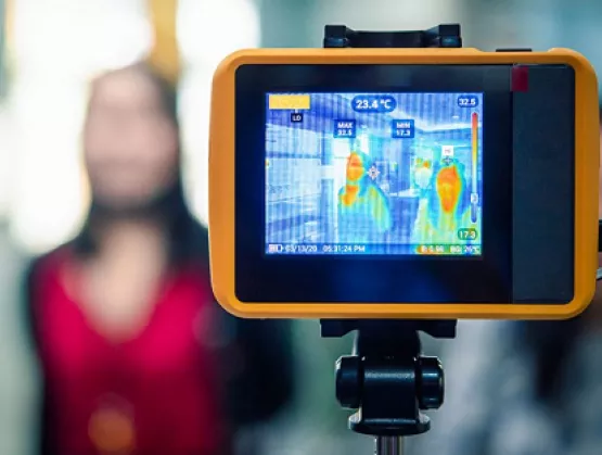
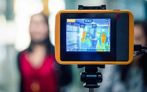
(The following is an excerpt of an article published by i-Micronews.)We are today entering a new era when sanitary checks will be regularly required to travel, do shopping, or have a social and cultural life. In this article and the related new Yole Développement (Yole) report, Thermal Imagers and Detectors 2020 – COVID-19 Outbreak Impact – Preliminary Report, we analyze how the COVID-19 outbreak could affect the thermal technology market and industrial landscape.To resume normal air traffic, air passenger screening to detect travelers with signs or symptoms of infectious disease will require new modalities. Thermal imagers could be used as a fast primary testing solution. This won’t be the first time actually. In the previous SARS, H1N1 and Ebola epidemics thermal cameras were used in some airports to screen travelers for fever. Of course, the size of the previous epidemics was not big enough to give this technology much attention. The way forward would be a triage process. Thermal imagers based on microbolometer technology can be installed at airports. If a fever is detected, then the traveler could be taken aside to get further tested with a more accurate handheld contactless thermometer. If the fever is proven, then they can be isolated for further examination, either a history check, and/or a diagnostics test, provided that it gives results in a reasonable amount of time.Airports are not the only places where thermal imagers can be the new norm. In April 2020, more than 50 Amazon warehouses had cases of COVID-19. Typically, workers were having their temperatures checked by handheld thermometers at the entrance. Amazon installed thermal cameras at some of their sites, which allows for faster screening. If needed, a secondary, forehead temperature check is performed if the employee is flagged from the camera, according to Reuters. Other companies that have explored using the thermal camera technology include Tyson Foods Inc and Intel Corp. Even some schools in China have started using them. This is an example of how businesses and infrastructure are turning to methods for containing the spread of virus by using technologies that previously went unnoticed by the general public.More businesses can adopt thermal cameras. In all countries, between 5% and 10% of enterprises employ more than 50 people, according to the OECD. To return to work, they could use thermal cameras to monitor body temperatures of employees as well. Here we are talking about cameras in the order of hundreds of thousands units.But this might not be enough. Everyone will probably want to have the ability to check their body temperature at any time. We have here a big market opportunity for integration of thermal imaging into smartphones or wearables. This integration has been in process for years. And it has long been perceived as the next sensor to be integrated in a mobile phone after pressure, inertial MEMS, or CMOS imagers. However, when 3D sensing technology was launched by Apple in 2017, all smartphone manufacturers focused their effort on this application, and were not interested in thermal imaging. Nowadays, because of the COVID-19 pandemic, people are much more sensitive to checking their own temperature and those of people around them, usually several times per day. Integration of a contactless thermometer could make sense. So there could be a revival of the use case of thermal imaging capability or temperature measurement in a smartphone or a wearable in the future.Click here to read the full article in i-Micronews.Eric Mounier Ph.D. is Fellow Analyst at Yole Développement (Yole). Dimitrios Damianos, Ph.D. is a Technology and Market Analyst at Yole Développement (Yole) working within the Photonics, Sensing Display division.Yole Développement is a member of SEMI and the MEMS Sensors Industry Group (MSIG), a SEMI Strategic Association Partner.
Read More
Olivier Corvez, senior manager of Environment, Health, Safety and Sustainability at SEMI, sat down (virtually) with Todd Patterson, vice president of global EHS for Entegris Global Operations, to discuss how Entegris has responded to the global pandemic.Corvez manages and Patterson participates in the COVID-19 EHS Task Force currently meeting weekly to discuss industry response and share best practices. SEMI: Was Entegris prepared for the COVID-19 pandemic? How did the company respond?Patterson: Entegris has a strong risk management framework and a risk assessment team of senior leaders who meet at least once a quarter. This focus gives us early visibility into events that could destabilize our organization or threaten our operations. Such a framework helps ensure we have the information necessary to act as soon as possible when the need arises. However, our business continuity plans for a pandemic of this scale were far less than with other more commonly occurring catastrophic events such as earthquakes or hurricanes. The COVID-19 crisis was clearly unprecedented and as such, the necessary systems and procedures were not in place with the depth and detail needed. Our strong governance structure made it possible for us to hold steady even as the pandemic caused increasing uncertainty and disruption around the world. For example, despite major supply chain shutdowns across many industries, to date, our supply chain and manufacturing operations have only been modestly impacted by COVID-19. Our supply chain team was assessing daily the areas of risk with our suppliers and taking appropriate action as well as preemptive steps to ensure our critical supply lines remained open.Our sales team engaged in regular communications with our customers providing them updates about our Business Continuity Plans and our actions to mitigate the risk to any of their deliveries. In addition, we maintained current information about the continuity of our supply chain on the company’s intranet for the global sales team to access as they engaged with customers. Also, a proactive communication plan was implemented immediately to send weekly video messages from senior executives directly to employees’ emails. It was an effective way to communicate with our global teams, to keep them informed about the status of the company’s operations and maintain a common sense of purpose at a time when many colleagues worked from home. In these weekly messages, we also focused significant attention on the health and safety protocols established to protect our manufacturing and lab employees from the virus.Among the health and safety protocols we implemented immediately as the virus moved across different regions were those related to facility screenings, work-from-home policies, social distancing, self-quarantine requirements, contact tracing, increased disinfecting, and travel restrictions. With approximately 5,300 employees worldwide, we had teams in every region ready to implement these comprehensive protocols. We believe we were among the first companies to implement work-from-home policies and travel restrictions.Temperature screening stations at Entegris facilities in Jangan, Korea (left) and Kulim, Malaysia (right). In addition, our CEO led a COVID-19 Steering Committee comprised of senior executives and managers from operations, human resources and communications. The committee met several times a week during March and April to evaluate and formulate responses to the issues that emerged as the virus spread from region to region. The committee’s work created a strong partnership among senior executives and divisional and functional leaders, and the initial guidelines developed by the committee have formed the backbone of a global playbook to limit the spread of the virus to our other sites around the world.Recently, the committee has changed its focus to more strategic issues such as creating a framework for transitioning remote workers back into our office locations. Meanwhile, local leadership teams at each of our global sites have been empowered to address ongoing tactical issues consistent with our thoroughly documented health and safety protocols.Looking to the future, we are using our experience in responding to COVID-19 to develop a more comprehensive pandemic response plan. We have project teams working on better ways to: measure temperatures of personnel entering our sites facilitate social distancing in the workplace redesign common use areas to reduce the number of high touch points disinfect all spaces thoroughly and regularly, and manage emergency pandemic supplies. SEMI: From the SEMI EHS survey, we noted that all members had a Business Continuity Plan. How effective has it been for deploying resources and adapting quickly and minimizing the crisis? Why or why not? Patterson: Because we have operations in China, Entegris experienced the impact of the virus immediately. We quickly formed two task force teams for our two primary facilities in the region. These teams developed the means for communicating key information to employees and started working on prevention plans to protect employees and comply with local requirements for when operations resumed. They met the challenges head on and found quick solutions. An example was finding an effective way of communicating to the employees for each location. Group chats were established through social media. It was this work that led to their success in getting approvals from local authorities to resume operations. Those plans have laid the groundwork on which our other sites around the world could build their response plans.The effective management of our global supply chain also stands out as a key success of the company’s Business Continuity Plan. Entegris has a highly complex supply chain with approximately 6,500 suppliers and a $850 million annual spend, and we ship work-in-progress and finished goods from over 90 sites globally.As I mentioned earlier, despite the virus crippling supply chains across many industries, Entegris experienced very little disruption to its supply chain. The supply chain team was able to accomplish this despite a 90% reduction in global freight capacity. A key factor in keeping goods flowing to our factories was the intensive work the team had done earlier to develop an in-depth understanding of the company’s top suppliers and to mitigate sourcing risks. They had established alternate sources, balanced the sources geographically, and placed inventory across our supply chain to buffer risk.The team also had integrated statistical modeling into reporting tools, which made it possible to reset safety stocks and logistics lead times quickly as conditions changed. And a supply chain digitalization provided one aligned and integrated view via dashboards, giving the company the ability to respond rapidly and to communicate in real time with our suppliers. We essentially had a virtual war room where we monitored the daily impact of the spread of the virus and could address bottlenecks and other issues immediately.SEMI: What lessons have been learned, so far? How do you see changes in your company’s operations in the future?Patterson: Institutionalizing what we’ve learned has already begun. Whether the measures implemented during the pandemic are temporary or become permanent is still to be determined. Regardless, the learnings need to be documented and available as a playbook for if – or when – the next pandemic occurs.Entegris is already working on a more comprehensive pandemic plan that will be based on five levels of preparedness. Level 0 will cover annual training requirements and management of emergency inventory of pandemic supplies. Level 1 will include early recognition of an outbreak, and then Levels 2-4 will include requirements for when specific response measures are implemented. Entegris also has formed the “New Normal” task force, which consists of leaders representing a number of disciplines directing the project teams previously mentioned to create a more comprehensive pandemic response plan. One of the project teams is working on improving the facility screening process that performs temperature measurement for personnel entering Entegris sites. The team is looking at the best technology to scan body temperature. As to whether this technology is employed only while COVID-19 is still active or becomes a permanent way of doing business, this is still being discussed.SEMI: EHS is involved in both providing technical support to protect individuals but also in making organizational changes to favorize social distancing. Could you explain some of the successes and challenges while tackling these two fronts?Patterson: Very early in the pandemic, Entegris established a work-from-home policy for non-essential employees. This significantly reduced the number of personnel and the potential for contact at the Entegris locations. Significant facility changes also were required. These included the design of facility screening booths and modifications to common gathering areas such as canteens, meeting rooms, prayer rooms, and smoking points. Physical markings were used to designate 2 meters distancing, and the seating in canteens and meeting rooms was reduced and staggered to minimize the risk of exposure to the virus. Entegris also has a project team focused on developing design solutions for offices and workstations when space makes it difficult to maintain 2 meters social distancing. These changes turned out to be essential for some sites in meeting mandates by local authorities. Our sites in Hangzhou, China and Kulim, Malaysia both were allowed to resume partial operations after demonstrating to government authorities the effectiveness of the preventative measures put in place. One particular challenge we are facing is the range of personal differences and awareness levels within the workforce – including those that don’t understand the importance of the new guidelines. We are working closely in advising supervisory staff to be aware of the need for employees to follow all health and safety protocols we have put in place, including social distancing. That preventative measure is the most difficult to make part of our new behavior – it is unnatural and inconsistent with our human nature, but it is critical to preventing the further spread of the virus.SEMI: How do you envision the progressive steps in deescalating to bring back “normal” operations? Patterson: I don’t know whether Entegris will ever go back to the old “normal.” As previously mentioned, we are working on the “New Normal.” Our focus now is on bringing our work-from-home employees back to the workplace without adding risk of exposure to the virus. We are still exploring options, but we expect to do it in a phased approach so that we can adequately assess the preventive measures that are in place and determine whether adjustments need to be made to any of our health and safety protocols.We are starting to see a variety of different frameworks emerge for evaluating repopulation timing and procedures. We will assess them on an office-by-office, or site-by-site basis, utilizing consistent criteria to define the potential for exposure to the virus. This also applies to our field service workforce. However, I have not yet seen any governmental guidance that offers a recommended framework for returning employees to the workplace. I think this represents an opportunity for SEMI EHS and the Standards groups to work to establish that framework for our industry.SEMI: Anything else you would like to share that you have observed throughout this crisis?We have not discussed the challenges faced in procuring and acquiring pandemic supplies. Almost immediately after the outbreak occurred in Wuhan, it became increasingly difficult to find supplies. Even when confirmation was provided by suppliers and delivery dates confirmed, the majority of the dates were pushed out or canceled. We found that what worked best was to have purchasing teams at the local site work with their local contacts on obtaining smaller quantities while a corporate point person was also managing larger orders. In preparation for any future pandemics, Entegris will be maintaining an emergency inventory for masks, sanitizer, thermometers, and disinfectants.For 18 months, Todd Patterson has held the position of VP Global EHS for Entegris Global Operations. His experience with emergency management and BCP has become invaluable in the past three months. He is grateful to his global response teams around the world for coming together to support the Entegris team in this unprecedented situation. Todd is an active participant on the SEMI EHS COVID-19 response teams led by Olivier Corvez at SEMI. Olivier Corvez is senior manager of Environment, Health, Safety and Sustainability at SEMI.
Read More
As government and business leaders start to talk about “returning to normal,” and looking to thermal cameras to help, questions remain about how and whether the latest technology can help prevent the spread of COVID-19.Across industries, everyone is looking for the right tools to help detect, slow and eventually stop SARS-CoV-2, the virus that causes COVID-19. By now we’ve all come to recognize that resuming operations in any way will require demonstrating measures to protect the health and wellbeing of people in a variety of situations, including travel and work.One proposed solution is thermal scanners. Unlike most medical imaging approaches, infrared (IR) thermography doesn’t require irradiation or expensive equipment, and presents no health hazard. Infrared radiation emitted from our skin can be detected and used along with information about the ambient environment to estimate core body temperature — which may indicate someone is running a fever, a common early symptom of COVID-19. While thermal cameras can’t detect a virus or a specific infection, they can help by quickly narrowing down a large pool of possibly infected individuals. And today, this represents the only viable non-contact mass screening approach for fever. The accuracy of the infrared system can, however, be affected by human, environmental and equipment variables. Understanding this multitude of variables — including the ways in which the science, technology and applications themselves interact — will help both users and system makers deliver the best results.Consideration #1: Think about the methodThermal detection has been used for fever detection for 20 years now. While older thermometers and thermal cameras, including the type used to detect a different coronavirus, severe acute respiratory syndrome (SARS), had their weaknesses, newer generations deliver significant performance improvements. More intelligent systems now offer features such as real-time calibration to ambient temperature with sub-degree °C accuracy, providing more accurate readings far more quickly than older generations.Newer camera systems are also more user-friendly and more reliable, featuring automated target recognition, improved resolution, pairing with a visible-light camera, automated alarms for febrile cases, and clearer outlining of hot spots. This higher degree of granularity improves insight, allowing for a more efficient and faster screening process, and provides on-site health professionals with necessary information to take additional steps when required. Advanced image processing features in new radiometric thermal cameras. Consideration #2: Know your baselinesBecause the environment can influence temperature measurements, some system makers have devised different ways to establish functional baselines. An early approach, recording a population baseline at each site on each day, proved too time- and resource-intensive. A newer approach, using a reference temperature source, or black body, offers evolutionary improvement. Designed to maintain itself at a specific temperature, the black body device allows the thermal camera system to automatically calibrate. Even better is a radiometric camera, which can intepret the intensity of an infrared signal reaching the camera. This requires more rigorous design and testing by the manufacturer, but it delivers much more precise measurements.Diagram of a fever detection system with black body emitter Consideration #3: Looking in the right place While thermal cameras can only detect surface temperatures, different parts of the human body more closely correlate with body temperature. Based on recent scientific research, the most reliable spot in the human face is the canthus, the small corners over the tear duct of your eye where the upper and lower eyelids meet. This kind of precise targeting requires accurate pixel calibration capabilities. The best surface target for estimating core body temperature: the canthus at the inner eye Consideration #4: Checking your performance Operating an IR fever screening system in the lab is one thing, but out in the field, the situation becomes more complex. Users need a camera system that is reliable and stable when it comes to critical performance factors like resolution, sensitivity and frame rate. Understanding the performance considerations when imaging a subject at a distance, for example, and realizing the minimum number of pixels required to get an accurate measurement are both essential in staging a fully optimal fever-detection platform.Consideration #5: Finding your way in the “wild west” of thermal imaging in early 2020People from the many industries that have been devastated by this pandemic – including travel, sports, manufacturing, food and hospitality, and entertainment — are looking for ways to reopen businesses safely while reducing the probability of a second wave of COVID-19. Deploying technology such as IR fever screening systems as part of a range of preventative measures will hopefully support that effort.As is the case with any promising emergent technology, there is a fair degree of chaos around the nuanced considerations of system design and performance. What standards apply to IR fever-screening devices? Which are being enforced? Who makes them? Will they work? IR camera manufacturers such as Teledyne DALSA and the expert system integrators we work with can play an important role in helping manufacturers and integrators to navigate this chaos, enabling us to work together to potentially save lives.For an even more in-depth look at this topic, visit this page, download our whitepaper Thermal Imaging Technology for Fever Screening, or browse.Jean Brunelle, product manager for infrared imaging, is a technical leader in sensor integration at Teledyne DALSA. He works on developing new image correction and calibration algorithms as well as qualification and production tests for the company’s visible and LWIR lines of digital cameras. Having earned a bachelor’s degree in engineering physics and a masters in surface chemistry, he has a passion for all things sensors, from how they work to how they are fabricated and used. His focus for the past few years has been on micro-bolometer-based LWIR cameras. Most recently, he was involved in the development and testing of Teledyne’s very own WLP micro bolometer and its integration into a thermal camera.Teledyne DALSA is a member of MEMS Sensors Industry Group (MSIG), a SEMI technology community that enables the MEMS and sensor industry to address common challenges, innovate and accelerate business results.
Read More
Linx Consulting and Hilltop Economics continue to monitor how the global economy impacts the electronic materials supply chain. Amidst the recent economic and revenue results releases, we have generated a series of potential scenarios for the next few years. These scenarios are based around sales of silicon wafers expressed in millions of square inches (MSI). Our work develops a multiyear forecast from the historic record of the SEMI-reported MSI demand by developing an econometric relationship with underlying demand drivers. Using this methodology, Linx Consulting and Hilltop Economics have introduced the following three silicon demand forecast scenarios: V-shaped global recession consistent with severe COVID-19 impact followed by a sharp economic rebound. Probability of approximately 40%. V-shaped global recession but with business and consumer behavior differing from the past recession in that there is much more aggressive spending on technology goods that softens the impact for semiconductors in 2020. Probability of approximately 25%. An extended COVID-19 impact developing into a U- or L-shaped global recession with an economic rebound delayed for several years. Probability of approximately 35%. In the few months since coronavirus hit the world, the economic prognosis for all major economies has worsened dramatically, although forecasts remain speculative given the rapid rate of change in the political and economic environment. The forecast changes in GDP since February 2020 of the G7 nations vary from -5.9% for Japan to -10.2% for Italy. These changes are closely linked to unprecedented declines in employment, consumer demand and industrial investment – all key drivers for wafer area demand. This leads us to believe there will be a significant reduction in wafer demand as these economic factors feed through the supply chain.Other leading indicators show dramatic drops in the global and regional economies taking effect at an unprecedented pace. These indicators have a loose predictive relationship for silicon wafer consumption and portend a rapid drop in demand.The demand picture for the semiconductor supply chain (be it wafers, materials, consumables or devices) is thus gloomy, and our models are currently showing Q2 to Q3 2020 reductions in MSI demand of between -11% and -28% depending on the scenario.In marked contrast to this depressing economic picture, the indications from the end-to-end semiconductor supply chain continue to be much more positive. Demand for silicon reported by SEMI increased in Q1 2020 by close to 3% from Q4 2019, while results from materials supply companies vary from slightly negative to record-breaking growth rates through the first three to four months of 2020. Added to this, reported revenues from WSTS for Q1 2020 ticked up 6.2% versus the prior year and the three large foundries in Taiwan and China showed continued growth of Q1 wafer area shipments and a 32.3% growth versus Q1 2019.Revenue and demand reports from leading device manufacturers remain on trend from 2019 with no indication of a precipitous change. Anecdotal reports of strong technology equipment demand to support people working from home and demand for medical devices in response to the pandemic can be substantiated somewhat by demand data although not convincingly.Reports from materials supply companies indicate that factories continue to be fully utilized, having been designated essential businesses, and that safety measures implemented against infection are largely effective.There are some indications of caution, however. The major public silicon wafer suppliers saw a 4% drop in revenues in Q1 over Q4, despite the reported strength in silicon area shipments from SEMI, indicating either ASP declines or some inventory effects.We are advising clients supplying materials into the wafer fabs and packaging supply chains to develop contingency plans for a sharp decline in product demand of as much as 28%, which may bounce back rapidly to 2019 levels or higher in early 2021. However, companies should also be vigilant of a slower than hoped for return to previous activity levels if the effects of the pandemic continue for an extended period.For further information please contact Mark Thirsk at +1 774-245-0959 or on [email protected] in engaging with the electronic materials supply chain? The Electronic Materials Group (EMG) is a SEMI technology community representing SEMI member companies that provide substrates, polymers, metals, organic and inorganic materials, chemicals, and gases developed for electronics manufacturing. Linx Consulting is a longtime member and supporter of the SEMI Electronic Materials Group.Mark Thirsk is managing partner at Linx Consulting. Duncan Meldrum is president of Hilltop Economics.
Read More