downloadGroupGroupnoun_press release_995423_000000 copyGroupnoun_Feed_96767_000000Group 19noun_pictures_1817522_000000Member company iconResource item iconStore item iconGroup 19Group 19noun_Photo_2085192_000000 Copynoun_presentation_2096081_000000Group 19Group Copy 7noun_webinar_692730_000000Path
Skip to main content
Default Banner Image

Technology and Trends

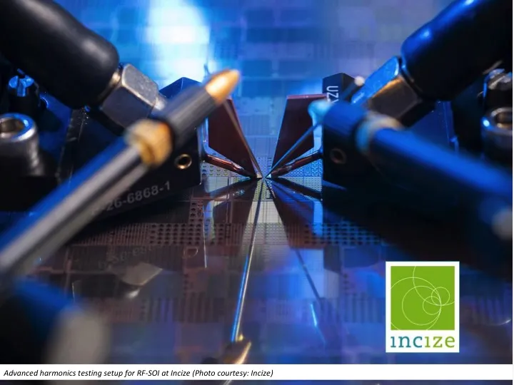
With the CAGR for switches in cell-phone RF front-end modules running at 9% for the next five years, new players want to get in on the action, and established players want to up the ante. The specialists at Incize help wafer suppliers, foundries and fabless companies maximize switch performance starting at the substrate level. CEO Mostafa Emam explains how.SOI News (SN): Can you tell us about the role Incize plays in the RF-SOI ecosystem? [caption id="attachment_32519" align="alignright" width="140"] Incize CEO Mostafa Emam. (Photo courtesy: Incize)[/caption] Mostafa Emam (ME): Our clients are wafer suppliers, foundries and fabless companies. The services we offer are testing and modeling of substrates, with the vision of what will happen in the value chain. Based on what the customer will do with the substrates, we do testing and modeling to improve the technology and tune their processes. Although the big players have teams devoted to this, we can add a layer of characterization that they have no expertise in. Some of our customers are foundries that have been using bulk silicon, but now see opportunities in RF-SOI. But they’re starting from scratch and we help them to adopt the technology. We help them understand the physics behind the technology so they can migrate from bulk to SOI. We help them develop test structures and evaluate their technology. Then we create models for both fully-depleted and partially-depleted SOI with PD-SOI 130 nm or 60 nm technology dominating the RF front-end module market. We believe RF is an art and you need to see the whole picture. SN: Can you tell us a bit about the history of Incize? ME: The RF-SOI story started in the 1990s. Then came trap-rich RF-SOI wafers from Jean-Pierre Raskin’s team at UC Louvain, industrialized by Soitec. Our lab at UC Louvain became known for our expertise in RF-SOI, and in 2011 we created Incize as a spin-off. [Editor's note: for more background, see this SOI Consortium article about the birth of trap-rich substrates and the company’s founding.] At first our characterization services were very diverse, but by 2014 we focused mostly on RF-SOI because of the big demand. In 2015 we started doing radiation hardness tests for space applications and a new business unit was created. In 2016 we started our modeling and PDK activity, followed the next year by work on GaN on Si. In 2018, we started offering full support to RF-SOI newcomers, who were starting from scratch, usually smaller players in the RF market. It takes about two years to fully train the engineers, support the technology enhancements, design test vehicles, measure them and finally do the modeling and PDK. So some of these players are now fully established in the RF-SOI market and have contracts in place with big customers. SN: In your presentations, you often say there is room for all. What do you mean by that? ME: There is a big market for RF-SOI in the coming years. It can offer the low-power, the low-cost and the high performance. RF-SOI is the only mature technology that combines all of this today. It successfully competes with traditional III-V technology. More foundries want to employ RF-SOI. We show to them that it’s not black magic – you just need to know how it works. [bctt tweet="There is a big market for RF-SOI in the coming years. More foundries want to employ #RFSOI. We show them that it’s not black magic – you just need to know how it works. - Incize CEO Mostafa Emam #5G #semiconductors" username="@soiconsortium"] On our side, we have the knowledge and the infrastructure. Our added value is that we can do advanced tests the customers can’t do. So the foundry says there’s opportunities in switches, we’ll do this and develop it all with optimization for specific Ron and Coff [the figure of merit for RF switches]. The foundry develops an RF switch and aiming at certain performance (RonCoff). We help our customers during this development phase. Once the performance target is reached we start developing a model and a PDK. There is enough demand for RF-SOI, as even entry-level cell phones have SOI chips. Some opt for a fast and low-cost solution. Many target “good enough”, although some target to compete against the big players – it’s a question of their business strategy. And this is where our added value comes in. SN: Can you provide some more insight into how you see the RF market? ME: The Front End Module (FEM) is a fast growing market, with increasing demand in terms of volume and performance. This includes antenna switches, LNAs, tuners, filters, etc. Historically, III-V materials have been used for their high performance and high power handling. However, RF-SOI has become the material of choice, and the biggest driver is integration of the RF switch and LNAs in one chip. It’s not easy to integrate the power amplifiers (PAs) on the same chip (still being on III-V substrates). But as it decreases footprint and cost, there are those who’ll do it. There is no viable competition for SOI – nothing will replace it in the short term. There are other technologies, but they are long term. It’s a stable market with high demand. SN: For those of us who are not RF experts, can you help us understand the technology? ME: The switch is sort of the traffic light of the FEM, receiving and transmitting. The simplest RF switch can be composed of only four transistors. Transistors leak power so you need to determine your Ron Coff performance. [Editor's note: Resistance on vs. Capacitance off, the RF switch figure of merit, is measured in femtoseconds and should be as low as possible. Psemi has a good video explaining it.] When the Coff capacitance is small, the switch is really off. When the On resistance Ron is small, it means low losses, and the switch is turned On. Ron and Coff is a compromise. And as there are many frequency bands and antennas, the FEM becomes very complex. Another issue is power handling, since the switch is the first stage behind the antenna. And finally, there is the question of switch linearity. Trap rich SOI wafers suppress harmonics so you have less distortion originating in the substrate. You have to model this – the designer needs to know. In addition to single tone harmonics you also get intermodulation, where, two or more high power signals at two different frequencies create distortion at other frequencies. The danger is that these parasitic signals can be so close that the filter can’t reject them and the useful signals get distorted. This was a killer for the switch created on the bulk substrate. Trap-rich RF-SOI fixed this. So now 100% of switches are on trap-rich SOI substrates. While it’s still a niche market, there is demand from customers for increasing the number of bands – that’s driving this market. SN: And what happens as we move to 5G? ME: There’s more and more pressure on the specs. It’s an art when anything changes. Moving from 3G to 4G required complete upgrade of the [foundry’s] models. With 4G, the specs are severe and the FEM must be built on trap-rich substrates. But 5G is not well defined, so the RF industry is taking their best shot. What is clear: the performance requirements get more challenging. Once the technology is understood, it can be implemented. But the foundries and the fabless need our help to do it fast and do it well. We create more value working together. SN: How do you see things evolving? ME: The number of foundries today doing switches on RF-SOI is increasing, and this will continue for the next few years. We saw this opportunity and invested in it. Our company is just ten people, and we are self-funded. We are swimming in business, but we have fun. And we’re getting recognition. Any company with CMOS in place could adopt RF-SOI. But it’s a different mindset. We help with the transition. ~ ~ ~Click here to read more feature articles in SOI News.
Read More
Part 2 of 2Read Part 1.While companies navigate the ongoing COVID-19 crisis, corporate leaders should be evaluating a number of key business continuity issues as well as steps they can take to not only react to business disruptions but also reshape their business and recovery plans.We spoke with Dan Steele, Senior Director and the APAC Head of Environmental, Health, Safety, and Security (EHS S) at GLOBALFOUNDRIES (GF) Singapore, via teleconference for insights into the best practices he and his team have implemented from their Business Continuity Plan (BCP) to guide them through the health crisis.SEMI: How can SMEs (small and medium-sized enterprises) afford BCP, as they are often quite costly?Steele: BCP is not something you afford. Rather, it is essential to good management. Every business is about managing risks and every manager’s responsibilities include risk mitigation. Regardless of their size, companies often pay a higher price for survival in a crisis because they are ill-prepared. All companies owe it to themselves, their employees and other stakeholders to conduct ongoing business continuity planning. No one knows what or when the next crisis will be, and no plan is perfect in mitigating crisis impacts.However, it is critical to plan for potentials, institutionalize EHS and security best practices, ensure the supply chain has both redundancy and robustness, train employees to adopt additional skills, and work with customers in advance. Companies that continue to ask themselves what if are the ones that will be the best prepared. And, if BCP is done right, businesses can avoid huge losses. Dwight Eisenhower said, "Planning is everything, the plan is nothing." I think too many companies spend far too much time creating exacting plans when instead they should be planning. Since planning the survival of the company is every manager’s daily responsibility, BCP should not be purely looked upon as a cost, but also as an expected deliverable from the management team.SEMI: Companies have rolled out mandatory work-from-home (WFH) policies and it has become a new normal for many of us. What other measures can GF take should this WFH period be extended?Steele: Our work-from-home policy seems to be working quite well at this point. However, WFH will only be effective if the right tools are provided to employees – we give our employees access to our system so they can work remotely. WFH also offers opportunities to drive new and innovative ways of working, and accelerates some of our automation efforts such as Augmented Reality (AR).At the same time, mental health is just as important and we conduct weekly check-ins with employees to assess their anxiety levels by asking two basic questions: How is the team’s morale and has it impacted productivity in our operations? For us at GF, WFH is not a disintegration of the team. It is important to our operations to continue the social aspects of working as ONEGF. That means online meetings should require face-to-face interactions. It is important for people to connect. Additionally, we maintain the same quality expectations for remote work as we do when employees are on-site. If this WFH period is extended, we need supervisors and managers to reach out and ensure that we stay connected with our employees.SEMI: What BCP lessons have you learned during the outbreak and will the learnings change any of your business or operations strategies when normalcy returns?Steele: I am not sure we learned anything new about BCP. As stated, our approach to BCP is to spend less time on exact plans and more time on planning, asking ourselves what if and mentally walking our way through potential solutions. This crisis reinforces the premise that we must be prepared. We did not have a plan on our shelf for working-from-home, but we had visualized it, knew what we would have to enact and now have employees managing highly sophisticated, technical and skilled manufacturing operations from home, and some of them reside in Malaysia. BCP must be a conscientious, concerted effort even when normalcy returns – it helps us better prepare. Additionally, BCP is not the responsibility of a single person or department. Just like our daily business, BCP is an integrated effort across many functions. Good and great ideas come from anywhere in a time of crisis. Listening is extremely important.SEMI: If there is one takeaway from this unusual and uncalled experience, what will it be?Steele: What we walk away with is the fact that we are dealing with a pandemic that is highly unpredictable, and that we need all types of employees with diverse backgrounds, experiences and perspectives. This inclusion has made us successful all along, and that is what is helping us ride through this crisis today and into tomorrow. We are glad that we have a diverse and proactive BCCM team that is able to quickly adapt and respond to the many challenges of a crisis. SEMI: What advice would you offer to stay productive while WFH?Steele: We acknowledged that it is difficult for the WFH policy to be effective in the manufacturing sector. Although we do not see any productivity loss thanks to automation, we’ve seen a slowdown in our engineering activities.My advice: First stay healthy, monitor your health, and follow the government’s hygiene advice for yourself, your families and the communities you live in. If you socialized before, there is no reason to stop. Stay connected with your co-workers and team. Personally, I don’t believe WFH now means you are always on. Just as you did when working on-site, you still need your personal time. You have to strike the balance that works best for you.Dan Steele has over 25 years of experience in environmental, health, safety and security operations. He has also held other leadership roles in facilities engineering, quality, reliability and assurance, and risk management.Bee Bee Ng is president of SEMI Southeast Asia.
Read More
The COVID-19 pandemic (caused by SARS-CoV-2) has disrupted lives around the world more than any other catastrophic event in living memory. Those of us fortunate enough to work from home are cheering on the people who care for our health, transport our packages, work in grocery stores and pharmacies, clean public streets and buildings, and keep utilities up and running — as well as everyone else on the front lines of battling this pandemic. Working from home also gives us time to reflect and ask: How does the world return to normal and how can we help?Crises like the COVID-19 pandemic accelerate social and technology trends because the need for new solutions grows urgent. Looking at epidemiological models can reduce complex disease progression to a series of simple numbers, the most important of which is R nought (R0) value. R0 is simply how many other people a sick person infects. If each sick person infects less than one person, R0 1, the spread of disease will end. But if each sick person infects more than one other person, the disease spreads and may become a pandemic. According to the journal Emerging Infections Diseases, SARS-CoV-2 has an R0 of 5.7, making it far more infectious than the influenza pandemic of 1918.Given the severity of the current pandemic, society has taken huge efforts to reduce R0: mask-wearing, social distancing, avoiding face touching, frequent handwashing and quarantines are all ways to reduce R0.Scientists and engineers are working hard to develop new solutions and evaluate existing technologies that could have a big impact on R0. One of these is the mass deployment of touchless technologies. We’re now aware that every time we touch a surface, we potentially spread disease. I have personally started using touchless Apple Pay at retail checkouts whenever possible and even seek out and remember which stores have enabled Apple Pay. Each time I need to touch an elevator button, security keypad or walk signal button at an intersection, I contort my arms to touch them with an elbow.Since I’m in the electronics industry, I find myself considering which devices have the greatest potential for reducing the number of touchpoints in our daily lives. Motion and ultrasound sensors are definitely promising, but the mainstream adoption of the voice interface makes it the most interesting and scalable touchless technology.New voice technologies are more reliable and secure than ever. The success of cloud-based voice assistants such as Amazon Alexa, Apple Siri and Ok Google has familiarized consumers with the ease and convenience of voice, but these high-powered AI assistants generally require high power and a reliable internet connection. The next wave of voice technology will be much lower in power, fast, private and require no internet connection. This edge-powered voice interface will not play music or tell you the weather, but it will perform many other useful and simple functions, such as operating an elevator, opening a door or changing the volume on your TV. One great example of this local voice command is the Simple Human trash can that can open and close in response to your voice. Opening and closing a garbage may be simple, but a voice-activated model enhances convenience and safety with total privacy.The requirements for deploying voice technology to support more touchless applications include: Low power — to run for months or years between battery changes Robust and reliable— to last over a decade indoors or out Locally processed data — to ensure security and privacy without an internet connection Consumer adoption of touchless and voice technologies has been growing for years, but the COVID-19 crisis highlights the critical benefit of these technologies in reducing the spread of disease. Making high touchpoints voice-powered would eliminate a disease vector and reduce R0 during pandemics as well as during normal cold and flu seasons. Any technology that helps reduce R0 should be deployed as quickly as possible to give us one more way to thwart the virus that is changing life as we know it.As the only supplier of piezoelectric MEMS microphones – which are natively immune to environmental contaminants such as water, humidity, salt, dust, dirt and oil — Vesper is uniquely able to provide outdoor-hardened microphones that are durable enough to support voice-interfaces in hot, wet, dusty or dirty conditions. In fact, we’ve earned the highest waterproof rating for any MEMS microphone – IP57 – which makes me hope that one day soon I’ll use just my voice to tell a crosswalk signal that I need to cross the street.Vesper has also developed a proprietary technology called ZeroPower Listening, which makes it possible to embed always-listening voice interfaces in battery-powered devices with battery life measured in months or years. And that’s just the beginning of how we’ll use voice interfaces in high-touch applications. From voice-controlled parking kiosks and elevator buttons to the treadmill at the gym, the less we touch hard surfaces, the safer we’ll be from picking up SARS-CoV-2, influenza viruses or other pathogens as we go about our daily lives.Learn how Vesper’s low-power and rugged MEMS microphone technology can help designers create seamless voice interfaces for a wide range of indoor and outdoor applications at Smart Home, Smart Office, IoT and Automotive/Industrial.Matt Crowley is CEO of Vesper Technologies, developer of the world’s first piezoelectric MEMS microphone. With five rapid product rollouts in just five years and tens of millions of units shipping to tier one clients across the globe, Matt has grown Vesper from a research-oriented startup to a bonafide commercial business.Under his leadership, Vesper has earned an impressive collection of awards including a 2019 Best of Sensors Award, Innovation Award nods at CES 2018 and 2019, and two Annual Creativity in Electronics (ACE) Awards.Before Vesper, Matt held leadership positions at piezoelectric MEMS pioneer Sand 9, the Boston University Office of Technology Development, and Mars Co strategy consulting, where he advised Fortune 500 companies on operational and strategic issues.Matt received an interdisciplinary degree in Physics and the Philosophy of Science from Princeton University. He is proficient in Japanese, having lived in Japan.Vesper is a member of MEMS Sensors Industry Group (MSIG), a SEMI technology community, that enables the MEMS and sensor industry to address common challenges, innovate and accelerate business results.
Read More
Part 1 of 2Read Part 2. While companies navigate the ongoing COVID-19 crisis, corporate leaders should be evaluating a number of key business continuity issues as well as steps they can take to not only react to business disruptions but also reshape their business and recovery plans.We spoke with Dan Steele, Senior Director and the APAC Head of Environmental, Health, Safety, and Security (EHS S) at GLOBALFOUNDRIES (GF) Singapore, via teleconference for insights into the best practices he and his team have implemented from their Business Continuity Plan (BCP) to guide them through the health crisis.SEMI: How did GLOBALFOUNDRIES Singapore first respond when the country reported its first COVID-19 case?Steele: Since the early days of our company, we have had a Business Continuity / Crisis Management (BCCM) team in place that is responsible for business continuity planning for the site. At the beginning of this journey with the coronavirus, we believed in two truths: maintaining the safety and well-being of our employees and consistently communicating precautionary measures the company has taken to protect them and our business. These actions are critical to keeping our employees safe, while keeping the anxiety level low. By informing and updating employees in a timely manner, we ensure that they are well-educated about the crisis as it unfolds and the foreseeable circumstances that could be ahead of us. Once the world was well into the coronavirus outbreak, our CEO declared in a message to all employees that “we entered this pandemic crisis together, and we will exit it together.”We have also established links to pertinent government websites and made them conveniently available to ensure employees have access to the latest available information for their personal lives.SEMI: What actions has GF Singapore taken in response to the crisis so far?Steele: On January 29, our BCCM team activated the first line of defense by initiating temperature checks at all building entrances for every individual including employees, contractors, visitors, and customers who come into our facilities. We asked each to declare their state of health and travel history and issued a temperature card to every employee and resident contractor. They are all required to record their temperature twice daily – once before coming to work and again at midday – and they present the temperature log to security upon their arrival.The following week, our teams split into an A/B work arrangement to ensure continuity of our operations. We proactively pared down our teams to the staff essential for our on-site operations, while enabling the rest to work from home. We also advised our most vulnerable employees with impaired immune systems or who are pregnant to work from home. Concurrently, we moved all meetings of 10 or more people to virtual communications and only allowed meetings with fewer than 10 to be held in rooms with participants sitting at least one meter apart. We informed our customers of our efforts and moved all planned on-site visits to online visits.In line with Singapore’s efforts to curb the spread of COVID-19 within the community, GF restricted site access of people who had recently traveled to countries with sustained community transmission and regularly updated the restriction list. To conduct contact tracing, we created our two degrees of separation list that we used to track employees with families and close associates who were linked to a COVID-19 case. Employees provided the information voluntarily. On our campus, we enforced strict safe distancing measures by limiting access to meeting rooms, marking off-limits tables and removing chairs in the cafeteria, limiting the number of elevator riders to no more than four, and placing boxes or other spacing indicators at smoking zones, bus stops and temperature-taking lines. We also initiated a daily log of employees taking the company buses tagged to the bus number, time, and employee identification numbers in anticipation of the need for contact tracing.Most recently, when the Singapore-Malaysia border closed, we activated the next phase of our BCP that was already in place – housing over 450 Malaysian employees in Singapore hotels.Throughout this crisis, we continuously monitor and evaluate possible impacts to our supply chain to ensure the continuity of our business. This is a standard element of our ongoing business continuity management system.Most importantly, we frequently communicate with our employees and tell them everything the company is doing and why we are doing it. We encouraged employees to monitor their health, stay home if they are unwell, and seek immediate medical treatment if necessary at one of our panel clinics or other medical facilities.SEMI: What are your top concerns amidst this health crisis?Steele: At GF, we are managing through the crisis with an unwavering focus on two guiding principles: the safety and well-being of our worldwide team, their families and communities; and delivering on our commitments to our clients. As the world’s leading specialty foundry, GF has a unique role in the global supply chain. Our semiconductor technology is vital to a range of industries including health care, communications, infrastructure and security. With these priorities in mind, the company undertook unprecedented steps and has adapted to the crisis by dynamically adjusting its protocols, health and safety measures, and business processes to protect its teams while maintaining manufacturing excellence.We are committed to safeguarding the well-being of our employees while supporting and sustaining our on-site operations and protecting customers’ products. A major concern is the impact on our employees. We understand that COVID-19 can be infectious even if an individual is asymptomatic – we are always concerned that temperature screening alone is not sufficient. This is the reason that from day one we have encouraged our employees to monitor their health, follow all government advice for proper hygiene and seek medical attention if unwell as early as possible, and not come to work.Dan Steele has over 25 years of experience in environmental, health and safety, and security operations. He has also held other leadership roles in facilities engineering, quality, reliability and assurance, and risk management.Bee Bee Ng is president of SEMI Southeast Asia.
Read More
The Compact Model Coalition (CMC) has selected Leti’s L-UTSOI as a standard model for FD-SOI in the industry. The CMC is a working group composed of the major semiconductor companies and is part of the Silicon Integration Initiative (Si2). The Si2 Compact Model Coalition announcement covers the approval and financial support of L-UTSOI. L-UTSOI is derived from the Leti-UTSOI compact model, which has been implemented in circuit-simulation software and used in industrial process design-kits for several years. Thierry Poiroux, head of CEA-Leti’s Simulation and Compact Model Laboratory, said the selection of L-UTSOI as a Si2-CMC standard model ensures that it will be supported as long CMC industry members use it. “This is of paramount importance for large chip makers who will use this model in the future,” he continued. “With a standard model, they are assured that a team of model developers is able to take care of the model improvements and/or bug fixes they need during the whole lifetime of their technology. It also positions CEA-Leti among the few compact-model developer teams able to develop and support a standard model.” The role of compact models Once a new or enhanced chip is designed, it must be simulated prior to entering the expensive manufacturing phase. This proof-of-concept step relies on compact models that are expressed through a set of equations implemented in a form ensuring accuracy, robustness and numerical efficiency. Such compact models are approved and supported by the standard-setting arm of Si2, the CMC, which is an international working group focused on standardizing SPICE device models. “As a member-driven organization, the CMC strives to provide value for its members and the semiconductor supply chain,” said Peter Lee, CMC chair. “With 15 models now available, CMC members have a distinct competitive advantage with early access to new features and bug fixes, and an 18-month lead on standard models released to the public. Adding L-UTSOI to the mix of models was a direct response to our customer requests for model support as we continue to add value to their membership.” Standard models are developed by the world’s leading SPICE-model experts. They are used by designers working at the most advanced fabless semiconductor companies, foundries, and IDMs. Implemented in the industry’s top versions of circuit-simulation software and duly qualified, standard models give designers the assurance that their integrated circuits will perform according to the design specifications. Industry proven L-UTSOI was extensively proven by the industry and its standardization will ensure long-term access and maintenance in EDA tools for FD-SOI designers. Available to coalition members now, it will soon be implemented in major versions of circuit-simulation software, and its source code will be released publicly in June 2021. “CEA-Leti’s compact model boasts physically based model parameters,” said Harrison Lee, chair of the L-UTSOI Working Group and principal engineer of the Foundry Design Enablement Team at Samsung Electronics. “We can utilize predictive analysis of a process technology to optimize a transistor’s design implementation for a specific end-use. With a capability to 10 nanometers and below and the ability to simulate a wide range of voltages and body biases, we can easily research a wide variety of analog and digital applications.” As noted in Leti’s announcement (read the whole thing here), the FD-SOI transistor’s back-gate allows tuning of the device in a low-leakage and low-power operating regime or higher-performance operating regime. This unique capability offered by FD-SOI enables the fabrication of smaller, faster and denser chips than standard bulk CMOS technology. FD-SOI devices are widely used in wearable electronics, automobiles and IoT. Leti pioneered FD-SOI in 1992. Here at ASN we’ve been covering their FD-SOI compact model work for over a decade.
Read More
Let’s celebrate! As of April/May 2020, Advanced Substrate News – or ASN for short, and now aka the SOI Consortium newsletter – has been bringing you news for 15 years. I hope you’ll forgive me if this post has a personal angle, as I have been the Editor-in-Chief since Day 1 back in 2005. One of the things I’ve learned over my career covering technology in general and SOI in particular is that “new” technologies are never really new. They don’t pop out fully formed like Venus Boticelli-style. They take years – decades, even. SOI is no exception. What is exceptional about SOI imho is that the ecosystem – from the substrate providers to the end-product designers – keeps finding new things to do with it. There have always been naysayers – and for a while it took on an quasi-fanatic ferocity. There were those who quipped that SOI was the technology of the future...and always would be. But as it turns out, SOI’s is, has been and will be the right technology at many right moments, and I don’t see any sign of that changing in the years to come. We Need a Newsletter! [caption id="attachment_32012" align="alignright" width="189"] My Design News piece on SOI from June 2000 - it changed my life![/caption] As so much in the SOI story, ASN began with Soitec. I first encountered Soitec when I was working as Contributing Editor in Europe for Semiconductor International in the mid 1990’s. It was a start-up of just a few people that made silicon-on-insulator aka SOI wafers. Most of us at the time had barely a notion of what that was all about, but they had an intriguing story to tell about higher performance and lower power. It so happened a few years later (circa 2000) I was also writing for another publication called Design News – not about chip design, but product design, for folks designing cars and consumer electronics and washing machines and such. I kept hearing a new requirement added to the product-design mantra of faster-smaller-cheaper: lower power. It seemed to me that these SOI wafers could go a long way in solving some of product designers’ challenges. I pitched a story to my editor and it wound up on the cover (those were the days some might remember when trade magazines were on paper…). The big players were IBM for digital (in a current-events aside, DKY that those big iron machines at the US national labs cranking on the solutions for the current pandemic use IBM FinFET-on-SOI chips? Just saying…), Philips (now NXP) for power/analog, and Soitec for wafers – and of course Honeywell for aerospace and the big electronics players in Japan for all sorts of things automotive and ultra-low power. Top management at Soitec read the piece and saw that I “got it”. They brought me on board as a consultant, writing early websites, PR, brochures and such. But also most importantly, they invited me “in” – I sat in on sales reviews and attended the big shin-digs they sponsored on the Riviera and in the Alps. The people I met there – and stayed in touch with – were many of the ones that drive the industry today. (Of course, that was then, this is now: I don’t have that insider status any more, but I’ve kept in touch with and often still rely on the expert advice of people I met during that heady time.) Anyway, one day at the end of 2004, the Soitec folks said to me, “We need a newsletter.” They asked me to come up with a concept they could pitch to the Board. Since Soitec was also doing GaN SiC at the time, I thought it should be called Advanced Substrate News – ASN for short. And we agreed it should involve the entire ecosystem: end users, equipment manufacturers, academics, suppliers of all sorts, and especially: chip designers. But it was not an easy pitch. Who’d want to read about SOI wafers, they asked? Wouldn't we run out of things to say after two or at most three editions? But the idea was a solid one: ASN could be a bully pulpit for the nascent SOI ecosystem. Happily it won the day. I was named Editor-in-Chief, and have held that title ever since. Our very first edition (we were a print quarterly then) had about a dozen articles on SOI, including automotive with Philips, ultra-low power FD-SOI with Oki for Casio’s G-Shock watches (oh yes – it goes back a long ways!), low-power (by a company that Arm then bought), high-performance, high-resistivity SOI wafers for RF…it was all there. And if you look at what we cover now, it’s still all there – albeit better than ever and growing fast. (I just listened to the most recent Soitec Q4'20 quarterly financial report audiocast – announcing that they’d just had their best quarter ever – largely driven by RF-SOI.) We Need a Consortium! In 2007, the SOI Consortium was created with 19 members (a dozen of whom are still members today). As ASN Editor-in-Chief, I was honored to be part of that effort, participating in the meetings where we hashed out what it was all about and what a consortium would do. It was a great opportunity to meet the movers and shakers across the industry, many of whom I’m still in touch with. We published steadily, as the years, technologies and applications came and some went, but ASN readership continued to grow worldwide. Then in 2015, I got an email from the head of the Shanghai Academy of Sciences, which had recently spun off an SOI wafer maker called Simgui. He was (and is!) an ASN reader (though now he’s China’s Vice-Minister of Science Technology). Would I come to Shanghai and present some of the SOI-based applications ASN had been covering to his team there? They’d been working on SOI in parallel for many years, and were interested in where it was going in Europe and America. That was exciting! My first trip (of many, now) to China, it coincided with Semicon China 2015 and the announcement of the “Big Fund”. It was hall upon massive hall of stands immense and tiny, and the level of excitement was nothing short of amazing. (I was one of the only Western journalists there, and essentially broke the story in a piece I wrote for Consortium member Applied Materials’ customer magazine). That trip opened a lot of doors for me and ASN. As the SOI Consortium teamed up to with partners in China to host symposia there, we devoted more and more extensive coverage in ASN to those exciting events. [caption id="attachment_32041" align="alignright" width="328"] Here's some of our core players at the SOI Consortium: Executive Co-Directors Carlos Mazure (also of Soitec) and Jon Cheek (also of NXP) on the far left and right, respectively, Event Manager Iris Rith in the middle, me (Adele Hars) next on the right. We're joined here by Lucy Dai (2nd from left) of Simgui.[/caption] Eventually in 2016, ASN moved under the aegis of the SOI Consortium. We’re quite a jolly band that I have the privilege of working with. Granted at the time of this writing, the world is a difficult place, with so much uncertainty. But there are exciting times ahead with new products and technologies enabled by SOI, and you can be sure we’ll be covering them. RF-SOI will continue its juggernaut path in 5G mmWave. FD-SOI is steadily defining the new mainstream at the edge. The huge amounts of data the world is generating is driving photonics (which is all about SOI) to new heights. SOI for power (meaning high-voltage – think smart power) and imagers continues to grow. [caption id="attachment_32045" align="alignleft" width="99"] That's me - Adele Hars, ASN Editor-in-Chief - at the SOI Consortium's 2019 FD-SOI Symposium. (Photo courtesy VeriSilicon)[/caption] I’m honored to have brought you ASN for the last 15 years. Our archives are truly a treasure trove, and our mailing list of over 2500 really is an industry who's who. We’ve published well over a thousand (!) pieces in that time, most of which I’ve written with guidance from many an expert. However, we of course encourage our readers to pitch stories and/or submit SOI articles for publication consideration - so please, don't hesitate! I want to thank you all for your interest and your continued support. And thank you especially to all the SOI experts out there who so generously – and so patiently – share their time and enthusiasm with me and our readers. Stay safe! With warm regards, - Adele P.S. If you're not already on our emailing list and would like to join, just fill in the form at the bottom of this page. Thanks!
Read More
As the world confronts the health crisis of a generation in the form of the fast-spreading coronavirus, the microelectronics industry remains firmly in the spotlight. Aware of the central role they play in the fight against the COVID-19 pandemic, a growing number of companies are joining efforts to combat the virus by developing technologies for coronavirus detection, contact tracing and predicting its spread.SkyWater Technology, a U.S.-based foundry and prestigious member of SEMI-Fab Owners Alliance, is on the front lines in supplying an essential microfluidic MEMS component used in COVID-19 testing and research to identify mutations of the virus. This component is instrumental for the sequencing kit in the DNBSEQ-T7 system, an ultra-high-throughput sequencing system manufactured by MGI, a subsidiary of global genomics leader BGI Group.SEMI had the pleasure to catch up with Thomas Sonderman, president of SkyWater Technology, to talk about the company’s valuable contribution to the detection of COVID-19. He also gave us a peek into its business continuity plan and the safety measures it is taking to resiliently run a 24/7 chip-making operation amid these unprecedented times.SEMI: Tell us about SkyWater's contribution to the detection of COVID-19 and your partnership with MGI?Sonderman: SkyWater has been working with genomics sequencing leader MGI for several years to supply a critical component used in MGI's DNBSEQ-T7, an ultra-high-throughput sequencing system. The component we supply to MGI is a microfluidic MEMS device that uses microscopic channels to help perform very small-scale chemical reactions in the genetic sequencing platform. MGI's DNBSEQ-T7 identifies and monitors possible mutations of viruses, which is important for epidemiologists when tracking how viral illnesses such as COVID-19 spread through human populations.MGI’s sequencing system is used in parallel with its sister company BGI Genomics’ RT-PCR test kit, which is typically used more broadly as an initial screening agent due to its ability to return virus detection results within a matter of hours. Sequencing with the DNBSEQ-T7 can be used to confirm results of the RT-PCR tests that have indicated positive for the presence of the virus and then to perform a full DNA sequence of these positive specimens, which can help track mutations in the virus.DNBSEQ-T7 is important in the fight against COVID-19 as it tracks how the virus changes and enables scientists to look at its genetic sequence like a fingerprint at a crime scene. Their focus is on finding sudden changes in the sequence over time — a mutation. When they analyze available genomes from infected patients in several countries, they can see if inevitable virus mutations are causing associated illnesses that may have different incubation periods, contagiousness or deadliness – all critical dynamics that must be tracked by public health officials during an outbreak such as this.SEMI: What was the path that brought your company to the forefront of this testing?Sonderman: MGI’s DNBSEQ-T7 sequencing system and BGI’s RT-PCR rapid testing kit were among the first officially approved products by the National Medical Products Administration (NMPA – essentially China’s version of the FDA) – to fight the outbreak. MGI’s manufacturing plant, based in Wuhan, was able to fast-track its response, producing and delivering test kits very quickly to many hospitals and disease control centers in Wuhan and other cities in China.As concerns continue to rise about COVID-19 and we strive to flatten the curve, the pressure is on to enable even faster, more accessible testing. On March 27th, BGI’s RT-PCR virus detection test received FDA Emergency Use Authorization (EUA) for use in the U.S. The test works in just three hours. MGI’s DNBSEQ™ T7 sequencers are being used in China and other countries now and will be available in the U.S. starting in Q3. Products from BGI/MGI and affiliates are currently being distributed to more than 70 countries and regions worldwide to assist the global efforts in fighting the pandemic.SkyWater is certified to the ISO 13485 Quality Standard for Medical Devices to support the design, development and fabrication of DNA sequencing and other biochip applications in a wide range of emerging biomedical market segments. This allows us to provide this type of cutting-edge technology solution that is making an important contribution to coronavirus detection.SEMI: Given the challenges COVID-19 has placed on workforce and supply chain, what steps are being taken by your company to mitigate disruptions? Sonderman: SkyWater has been identified as Essential Critical Infrastructure per the U.S. Dept. of Homeland Security in several categories including Healthcare/Public Health Sector, Defense Industrial Base Sector, Information Technology Sector, and Critical Manufacturing Sector. To maintain continuity of operations, we contacted our close market partners as we need their support to continue supply of their starting and manufacturing support materials necessary for us to maintain operations. We asked these organizations to make every reasonable effort to fulfill our order requirements while also following recommended protective measures and are actively monitoring these relationships for possible developments that could be disruptive. By means of their partnership with us, these suppliers, too, are a part of the Essential Critical Infrastructure. Currently, there has been no change in wafer operations or fab utilization during this time of COVID-19.In addition to our sustained operations, our fab expansion is well underway as construction continues. The over 60,000-square-foot facility expansion adds clean room area and infrastructure to support the Department of Defense’s investment in SkyWater to broaden our production capabilities for Strategic Rad-Hard electronics and other complementary technologies. A fab technician in SkyWater’s SkyTech Center, an expansion of its operations to enhance advanced processing capabilities at its U.S.-based and U.S.-owned manufacturing facility. SEMI: What advice would you give to other companies seeking to keep their operations running amid COVID-19?Sonderman: First and foremost, creating a Pandemic Response Team (PRT) was critical for us in planning how to operate and communicate during this crisis. Our PRT updates our leadership team multiple times per week to enact procedures and ensure alignment throughout the organization. We follow CDC alerts and other local, state, and federal government guidelines on how to deal with home and work environments while communicating with all company stakeholders. This is important in providing reassurance of the company’s continued business and details on any potential change in operations.Increasing the frequency of communication with the organization’s supply chain to anticipate any disruptions in service is vital. Also, keeping in contact with customers is imperative to take the pulse of their continued operations during COVID-19. We recommend being flexible and pursuing new paradigms in getting business accomplished, such as telecommuting. In addition, if a company is deemed an essential business, we suggest drafting a letter in advance for employees should they need to prove why they are in transit (to and from work) if transportation becomes severely limited and monitored.Communicating with employees on how operations are changing is crucial. Ensure there is an intranet site that employees can access remotely via laptops or mobile devices that allows for ongoing updates and a way to communicate to all employees as things continue to evolve.We also put several safety measures in place, including: A screening process was set up to take the temperature of everyone entering the building. Site access is restricted for vendors, contractors, customers and other visitors as a default policy. Employee travel is restricted. All employees who can do their jobs from home can stay home. For essential on-site workers, we allow flexible schedules so people can move shifts if needed. Shifts have been staggered so people are not congested at lockers, gowning areas and other places. Physical distancing is required everywhere inside and outside the building. Video conferencing is being used even for participants inside the building. The number of people allowed in conference rooms is limited to comply with physical distancing; some chairs were removed and maximum occupancy signs were posted. Hand-sanitizing stations have been set up. We are providing employees access to masks, gloves and cleaning wipes. Safety measures are posted around the building and cleaning frequency of hard surfaces has been ramped significantly. These safety measures are among several other modifications we’ve made to daily operating procedures. SEMI: Please share some examples of how the SEMI Fab Owners Alliance (FOA) has helped support your business?Sonderman: Our Pandemic Response Team has leveraged the FOA recently by participating in its webinars on COVID-19 to ensure we are using industry best practices. We also use FOA surveys to provide and request information pertaining to COVID-19 practices.We have implemented building entrance protocols (i.e. temperature scanning, restricting access for non-employees) and expanded building cleaning procedures, including increasing the cleaning frequency of specific high-touch items. We have adjusted shift start times to minimize the number of personnel in the change room at the same time and we store each fab worker’s hood in the sleeve of the suit. These last two items resulted from a conversation with another FOA member.Outside of the pandemic, we have leveraged the FOA by participating in its industry-wide maintenance best practices and learning group that meets monthly on maintenance needs, issues and concerns within the industry. This allows us to learn from each other within the semiconductor industry. We have also leveraged this group in sourcing parts and/or parts sharing on tools no longer supported by OEMs.We greatly value the type of cross-organizational sharing and learning the FOA facilitates. It has been beneficial in a number of ways over the years. At this time, the FOA is especially useful when best practices are crucial to enable us and our peers to minimize disruptions, operate with the utmost safety, and quickly adapt to this new environment.SkyWater is a member of the SEMI Fab Owners Alliance, an international group of semiconductor and MEMS fab managers and industry suppliers that meets regularly to solve common non-competitive manufacturing issues and improve their business results. Nishita Rao is a product marketing manager at SEMI.
Read More
A recent survey by a SEMI Environment, Health and Safety working group found that all responding companies had Business Continuity Plans (BCP) in place prior to the COVID-19 outbreak, nearly half had already developed pandemic playbooks and, as a whole, have mounted robust, effective responses to the pandemic.The Business Continuity Plans of the 19 respondents to the survey, designed to speed crisis response and mitigate business impacts, included countermeasures for any threat to company operations including IT, production, finance, public communications and, of course, health and safety.Nine businesses, or 48 percent, had previously established plans for responding to epidemics and pandemics cited the World Health Organization (WHO) among the most reputable authorities for advice on how to prepare for a virus outbreak. Asian companies significantly outnumbered businesses in the U.S. or Europe in having a pandemic plan in place.The SEMI working group launched the survey shortly after it was formed in early March to gather insights into how SEMI member companies are protecting their employees while adapting facilities and manufacturing schedules to sustain production. The working group, which has grown to include 20 members that convene weekly for virtual meetings, consists of companies spanning the global semiconductor supply chain. The survey also found the following: As of late March, 95 percent of companies had implemented a mandatory work-from-home policy for job functions that could be performed remotely. One company reported that adherence to the policy was voluntary but strongly encouraged. At the time of the survey, 90 percent of companies had not considered using electronic tracking devices for employees at risk of cross-contamination. Taiwan has deployed the technology effectively to track confirmed COVID-19 cases and their travel histories. Nearly 75 percent of respondents conduct temperature screening for employees, 84 test visitors and contractors, and about 75 percent use no-touch infra-red thermometers as their preferred testing method. In instances where an employee, family member or close contact is ill but not a confirmed COVID-19 case, 42% of companies instruct the employee to stay home until he or she and family members are both symptom-free for at least 72 hours. For 30% of companies, the employee is invited to stay home for at least 14 days until the worker and family members are symptom-free. Fifty-eight percent of companies offer limited field service engineer (FSE) support to customers based on the circumstances. At 21% of companies, FSEs and equipment installers are working without restrictions if government and customer policies allow. Three companies suspended service activities. Sixty-three percent of respondents allow only critical visitors to enter their facilities after they’ve completed a health questionnaire and their temperature has been checked, while 21 percent prohibit visitors from entering their sites. More than half of the companies maintain production with social distancing protections in effect. For more information about the survey or to join the EHS Working Group, please contact Olivier Corvez at [email protected]. To learn more about best practices from SEMI member companies, visit our COVID-19 Resource page.Olivier Corvez is senior manager of Environment, Health, Safety and Sustainability at SEMI.
Read More
As a leading TCAD provider, Silvaco has very deep SOI roots, reaching back over 20 years. When Oki* pioneered the first FD-SOI chips in 2000 (really? yes!), whose tools did they use? Silvaco's. And those early FD-SOI chips went into Casio's most advanced G-Shock watches in 2005. (Yes, ASN has been covering FD-SOI for a long time!) But note that while those earliest chips used fully depleted architectures, they were on regular – not ultra-thin – SOI wafers, as they are today. [bctt tweet="Deep Roots: When Oki pioneered the 1st FD-SOI chips in 2000 (really? yes! for #CasioGShock) look whose tools they used: @SilvacoSoftware #FDSOI #lowpower #chipdesign #semiconductor #semiEDA" username="@soiconsortium"] When we look at the IEEE Spectrum Digital Library, it’s clear that Silvaco is continuing to be very active in the SOI space. There are 72 conference and journal publications citing Silvaco for their SOI research simulations since the year 2000 and 27 in the last five years. They’ve supported all the SOI evolutions – including partially-depleted SOI up through and including today's FD-SOI on ultra-thin SOI wafers. There are two Silvaco presentations that were given in Japan last fall – they're now on the SOI Consortium website. A Bit More About Silvaco Headquartered in Santa Clara, CA and founded in 1984, privately-held Silvaco is a leading provider of TCAD tools. TCAD (short for Technology-Computer Aided Design) is the use of computer modeling and simulation in developing semiconductor devices and processes. As such, TCAD tools reduce the development cost and shorten the development time. Silvaco also provides a full suite of analog and custom design tools spanning schematic, layout, signoff and variation analysis. The portfolio also includes tools for power integrity sign off, reduction of extracted netlist, and production-proven IP cores for automotive, consumer, and industrial applications. Silvaco provides a full TCAD to custom circuit design flow for vertical markets including: displays, power electronics, optical devices, radiation soft error reliability, analog circuits, library and memory design, advanced CMOS process, and IP development. They have 500+ customers in worldwide, and market leadership in TCAD design solutions for flat panel displays and power devices. Recent SOI Presentations Here's a quick recap of the two Silvaco presentations from the Japan SOI Symposium, October 2019, which you'll find on the SOI Consortium website. (To view the full presentations, however, your company needs to be a member of the Consortium.) Silvaco RF-SOI TCAD Solution was given by Sun Tao, Applications Engineering Manager, Silvaco. Silvaco positions itself as a “cost-effective partner to the FD-SOI community.” And as the presentation title indicates, it's a review of the tools Silvaco offers that support SOI – especially for RF applications. The presentation began with a review of recent updates to their TCAD simulation framework, including the TCAD design flow, Victory Process for speeding up 2D/3D process simulations, and Victory Device for device simulation. Under Silvaco’s DTCO – Design Technology Co-Optimization – flow, semiconductor physics are connected to circuit design, recognizing that each technology has specific requirements that need to be taken into account at every stage of the flow. [caption id="attachment_31635" align="aligncenter" width="589"] An example of how Silvaco Victory Tools Support Detailed Simulations of RF Devices on SOI (Courtesy: Silvaco and the SOI Consortium)[/caption] Tao then continued by showing useful TCAD simulations and analysis of SOI for RF applications. In trap-rich substrate simulations, for example, the Silvaco tools can predict the distortion from the active device, device biasing, and substrate, all of which can be co-optimized using Victory Process and Victory Device. In conclusion, he notes that Silvaco is offering TCAD to custom EDA solutions for predictive and comprehensive FD-SOI design work that can save money before committing to silicon. Platform Infrastructure for SOI-IP Ecosystem was given by Thomas Blaesi, VP of Global Marketing, Silvaco. "The massive use of IP is both an advantage and a challenge," began Blaesi. There are solutions out there, but they are disconnected. Typically SoC/IP designers, IP librarians, and support folks use various systems, while procurement, finance, and legal use others. This is a problem for both the providers and the consumers of IP. Silvaco has a system called Xena that centrally organizes all IP data: it’s an IP repository for tracking accounts, products, contracts, devices, support, compliance, and reporting. One of the first beneficiaries of Xena will be the SOI ecosystem, as providers of SOI IP are already signing on. [bctt tweet="One of the first beneficiaries of the Xena IP repository from @SilvacoSoftware will be the SOI ecosystem, as providers of SOI IP are already signing on. #FDSOI #RFSOI #semiconductorIP" #lowpower #chipdesign username="@soiconsortium"] Beyond the organizational advantages, Xena has patented “finger printing” and “DNA analysis”, so there is a digital representation of each IP on an SoC that cannot be reverse engineered. Each fingerprint contains list of unique signatures of each file in an IP or SoC. A file’s unique signature is created from the entire file content, and that signature is guaranteed to be unique to that content. [caption id="attachment_31634" align="aligncenter" width="591"] Silvaco's Xena Supports Audits of IP Usage in SoC Projects (Courtesy: Silvaco and the SOI Consortium)[/caption] It enhances support for all versions of common design files: hard IP, soft IP, and embedded software. Because it’s enterprise based, it will be particularly useful for large organizations. Fingerprinting and DNA analysis are vendor agnostic, universal, and easy-to-use tools and methodologies for IP lifecycle management, he concluded. -- *Oki's now part of Lapis Semi, btw, which is still active in FD-SOI

Read More
For five days in the latter half of March, the pall of the heavy human and economic toll COVID-19 has exacted in China appeared to be lifting. The epicenter of Wuhan reported no new coronavirus infections through domestic transmission. And in an initial step to loosen its nationwide lockdown, China began reversing restrictions on travel within its borders.Now, in another sign of progress, the region’s idled factory workforce is preparing to return to the production lines. Outside of Hubei province, home to Wuhan, most manufacturing workers are expected to be back on the job by the end of this month, with the proportion of manufacturing employees returning to work in Hubei cities except Wuhan reaching 70 percent by then, said Didier Chenneveau, Partner, Supply Chain Practice, McKinsey Company, in a late-March webinar presented by the business consultancy and SEMI.McKinsey is also “seeing evidence of a rebound in demand led by China’s online sales” as rising consumer confidence and a surge in the popularity of work-from-home policies spur strong spending on laptop computers, Chenneveau said.The turnaround stands in stark contrast to the unprecedented drop in demand McKinsey saw across retail and durable goods in China early in the year. Over the first two months, passenger car sales plunged 90 percent, smart phone receipts 40 percent and retail sales 21 percent, leading to what Chenneveau calls a whiplash effect that could disrupt supply chains as manufacturers and shipping companies scramble to meet pent-up demand once a recovery takes hold. As the outlook for China’s factories and suppliers brightens, concerns are shifting to the ripple effect of its deep manufacturing pullback on demand for goods in the United States and Europe. Sharp disruptions to global supply chains caused by labor shortages and knotty logistics challenges have also become worrisome. And while China is buoyed by the prospect of normalizing its workforce and manufacturing capabilities, parts shortages are bottlenecking production. In the United States and Europe, where 60 percent of air freight is carried in cargo holds of passenger aircraft, logistics concerns loom large with the widespread flight groundings. “Logistics must be a priority in any crisis war room because it’s a big challenge,” Chenneveau said.Asia Semiconductor Supply Chain ImpactsIn Asia, the semiconductor supply chain is working to overcome intractable challenges caused by COVID-19 including sourcing raw materials for chip manufacturing and maintaining assembly and test operations, Mark Patel, Sr. Partner Semiconductor Practice Lead, McKinsey Company, said at the webinar. Those problems cascade to foundries and IDMs even as they confront the compounding issue of a shortage of fab operators and engineers. Downstream, the inability to package, test and qualify products risks exacerbating the supply constraints.Patel said another acute challenge is that most semiconductor manufacturers and suppliers are operating under restricted practices, making it harder to sustain engineering activities vital to new product introductions, new process development and capital equipment expansion. In the longer term, the supply chain fallout hold implications for product life cycles and investments in capacity and next-generation technology – factors that analysts will need to monitor in evaluating the economic impact.Returning Workers Key to Economic RecoveryIssuing shelter-in-place orders have been an effective antidote to the spread of COVID-19 but a double-edged sword as nations worldwide sustain the economic blowback. Discretionary consumer spending on items such as automobiles has dropped by 45 percent globally so far this year, business investment has fallen and trade has seen a sharp slowdown, said Sven Smit, Chairman and Director at the McKinsey Global Institute, speaking at the webinar.A lockdown for as little as a month can slash aggregate global GDP by as much as 10 percent, a scenario McKinsey expects to play out in the second quarter of 2020. The drop would be the deepest since World War II and larger than the plunge in the first quarter of the Great Depression, raising the question of how long governments can afford to keep workers holed up at home.“The economic shock is unprecedented,” Smit said. “We’ve never sent people home to not work. Even in World War II, next to the front lines, people were harvesting food.”China offers a potential blueprint for economic recovery. McKinsey estimates that China’s rigorous containment efforts could help its economy bounce back in as little as six months – a V-shaped rebound. Western nations generally have not been as forceful with their containment measures. For them, the fight against the pathogen could be prolonged, deepening the economic damage.Yet even with the best protective lockdowns, a new challenge arises: The longer shelter-in-place orders remain in effect to contain the spread of the virus, the longer the economic impact drags on. “Until the path to return to work becomes clearer, people will not be confident to spend,” Smit said.Confronted with that reality, governments worldwide must strike the delicate balance between safeguarding the lives of people – critical forces of economic growth through consumer spending – and limiting the economic shock. The faster the virus can be brought to heel, the softer the impact to economies around the world. And the stronger the return-to-work protocols in place once COVID-19 has been brought under control, the faster workers can get back to their jobs. Smit believes resolving both issues simultaneously is not only possible but necessary for a return to normalcy.“That’s the imperative of our time,” he said. Related blog COVID-19: The Way Forward – Insights from McKinsey Company For McKinsey’s latest insights on the coronavirus pandemic, visit its website, which is updated daily.For the latest COVID-19 information and SEMI event updates SEMI is providing members, visit Coronavirus Resources.Michael Hall is a marketing communications manager at SEMI.
Read More