downloadGroupGroupnoun_press release_995423_000000 copyGroupnoun_Feed_96767_000000Group 19noun_pictures_1817522_000000Member company iconResource item iconStore item iconGroup 19Group 19noun_Photo_2085192_000000 Copynoun_presentation_2096081_000000Group 19Group Copy 7noun_webinar_692730_000000Path
Skip to main content
Default Banner Image

Technology and Trends

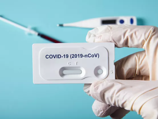
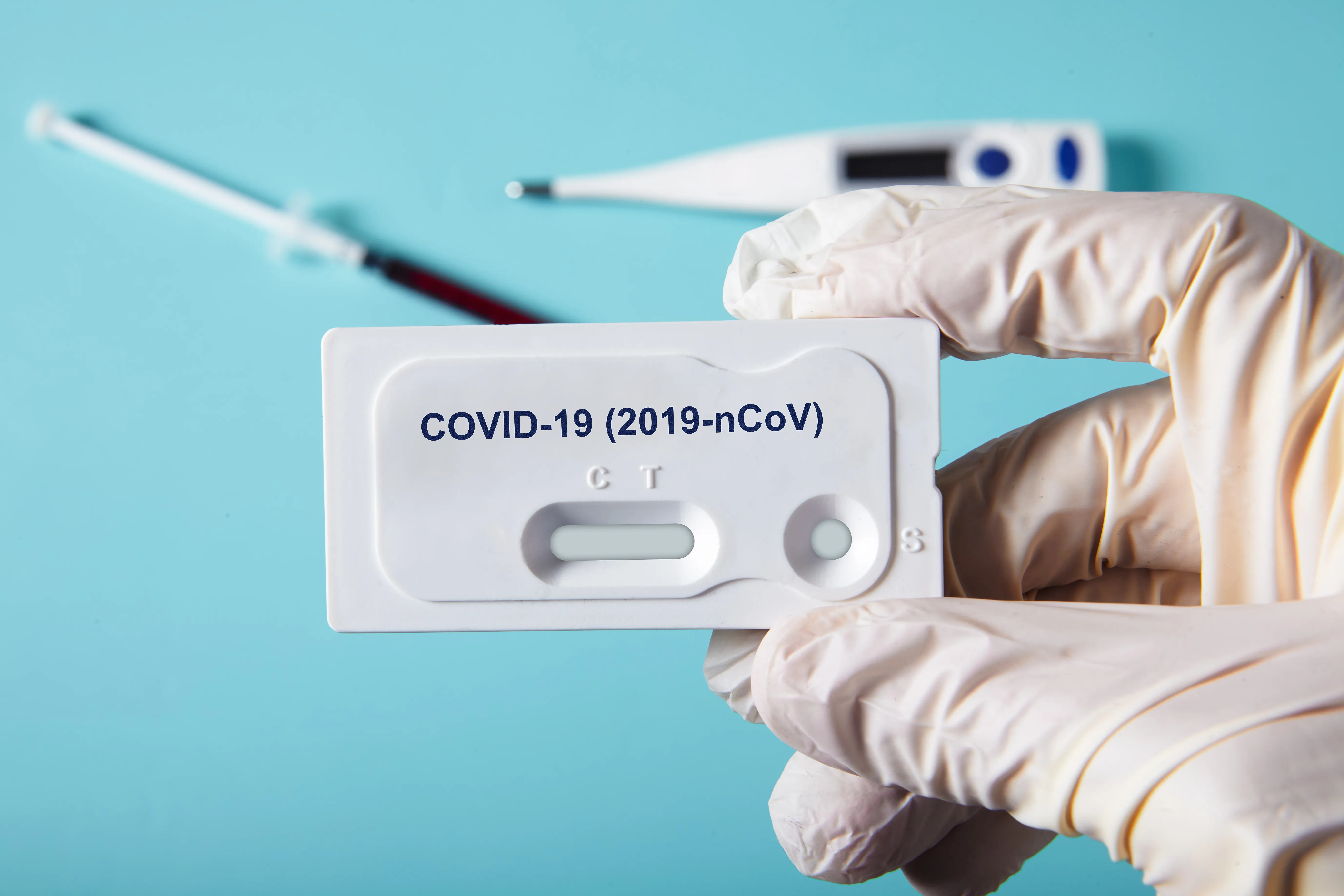
On Saturday, March, 21, 2020 the U.S. Food and Drug Administration (FDA) gave emergency authorization to Cepheid, a California company, to sell a new test for rapid detection of the pandemic coronavirus SARS-CoV-2, which causes COVID-19. Cepheid’s Xpert® Xpress SARS-CoV-2 test gives healthcare workers results in just 45 minutes, with less than a minute of hands-on time for sample preparation.Cepheid, founded by Kurt Petersen, M. Allen Northrup and five others in 1996, is well known in the MEMS community for commercializing microfluidic chip-based polymerase chain reaction (PCR) analysis machines. This is not the first time Cepheid has responded quickly to a biological threat; after the 2001 terrorist attacks in the USA, Cepheid was the first to provide rapid anthrax detection capabilities to the U.S. Postal Service, and it still does today.At the heart of all COVID-19 test protocols (see the WHO protocol and U.S. CDC protocol) is the real-time reverse transcription polymerase chain reaction (RT-PCR) analysis technique. In a very simplified description, PCR uses thermal cycling to amplify the DNA present in a patient’s swab sample, and then using fluorescence optical detection, searches for the virus’s specific DNA. The test requires knowing the virus’s genome in the first place; the crucial work to sequence the full genome of SARS-CoV-2 was first published by Chinese scientists for public use on January 10, 2020.While traditional PCR machines take many hours to thermal cycle and reach a result, MEMS-based PCR systems can work much faster. Featuring scale heaters and reaction chambers that have a tiny thermal mass, they create a significantly faster heat-cool cycle, enabling a rapid result in minutes.The first MEMS silicon PCR chip, developed by Northrup et. al. at Lawrence Livermore National Laboratory and licensed to Cepheid (left) and the Cepheid test cartridge today (right). (Source: Northrup MA, Ching MT, White RM, Watson RT, “DNA amplification in a microfabricated reaction chamber,” Transducers 1993, Yokohama, Japan. pp. 924–926.) Research on MEMS-based PCR systems has continued steadily since the early 1990s. Today, researchers have been focusing on developing highly integrated, low-cost systems specifically for point-of-care use. One example of recent research: a team at Korea’s ETRI and Genesystem have developed a prototype low-cost, handheld PCR system having a polyimide chamber and microheater and an integrated CMOS detector for optical readout of results (figure below). Cross-section schematic of the chamber, heating module and integrated optical detector in a portable PCR prototype (left) and integrated test cartridge (right). (Source: DS Lee, OR Choi, and YJ Seo, “A Handheld and Battery-Powered Realtime Microfluidic PCR Amplification Device,” Transducers 2019, Berlin, Germany pp. 1063-1065.) Korea’s quick recruitment of its biotech companies and creation of novel drive-through testing sites helped it to successfully pinpoint its COVID-19 outbreak and to implement control measures. Let’s hope the Cepheid test can be similarly effective.Based on successive epidemics of SARS, MERS and now COVID-19, rapid PCR test machines, enabled by MEMS technology, are becoming essential medical tools in the fight against viral outbreaks. As continued development lowers the cost of such critical equipment, let’s hope we may soon have a PCR machine in every doctor’s office.Alissa M. Fitzgerald, Ph.D., founded A.M. Fitzgerald Associates, LLC (“AMFitzgerald”), a MEMS and sensors solutions company based in Burlingame, CA, in 2003. She has over 25 years of engineering experience in MEMS design, fabrication and product development.Prior to founding AMFitzgerald, Fitzgerald worked at the Jet Propulsion Laboratory, Orbital Sciences Corporation, Sigpro, and Sensant Corporation, now part of Siemens. She received her bachelor’s and master’s degrees from MIT and her doctorate from Stanford University, in Aeronautics and Astronautics. Fitzgerald has numerous journal publications and holds eight patents. She served on the Governing Council of MEMS Industry Group from 2008-2014 and was inducted into the MIG Hall of Fame in 2013. Fitzgerald serves on the Board of Directors of both Rigetti Computing and the Transducer Research Foundation.AMFitzgerald is a longtime member of MEMS Sensors Industry Group (MSIG), a SEMI Strategic Association Partner. For more information on AMFitzgerald, please visit: https://www.amfitzgerald.com.Interested in learning more about this topic? Read Alissa M. Fitzgerald and Farzad Khademolhosseini’s article in EE Times, MEMS in the Fight Against Covid-19.
Read More
The seemingly simple act of commanding consumer devices by voice is a choice that nearly 118 million Americans now make every day, according to a recent report from eMarketer, the digital marketing research firm.While the voice interface is convenient for users, its implementation comes at the potential loss of individual privacy. The reason? Always-on, always-connected voice-first devices such as Amazon Alexa and Google Home require a wall plug and an internet connection to powerful cloud processors, making it possible for cloud companies — however benignly — to collect data on personal habits, location and conversation that were never intended for sharing. Move processing to the edgeTo address concerns over user privacy, device designers are attempting to do more of the audio processing within the consumer device, rather than sending users’ voices into the cloud. Moving more processing to the edge is a trend across the Internet of Things (IoT) industry, and not just for voice data but for other types of sensitive or proprietary data as well.Yet designers have realized limited success because the conventional approach to always-listening edge processing is notoriously inefficient: It digitizes and processes 100% of incoming sound data even though up to 90% of the data is irrelevant noise. This digitize-first approach wastes vast amounts of system power digitizing and analyzing the audio signal as it searches for a wake word when there isn’t even speech present, making it impractical for use in small, battery-operated devices.Workarounds don’t workTackling this power issue is critical to keeping private data secure. Unfortunately, it’s also exceptionally difficult. Design engineers have tried workarounds to decrease power consumption in an always-listening system, including duty cycling and reducing the power of each individual component in the audio signal chain that handles the data. The reality is that these kinds of approaches don’t address the root cause of the problem: too much data.To truly tackle the problem, we need to change our approach to a system solution, not a component solution. By moving to a more efficient edge architecture that intelligently minimizes the amount of data that moves through the system, we can focus the system’s energy resources on analyzing voice and not on searching for a wake word in irrelevant noise. Analyze, THEN digitize It’s time to move away from the digitize-first approach that has dominated voice wake-up device architecture since the invention of voice-first applications.Inspired by the way the human brain efficiently filters incoming information, differentiating, for example, a dog bark from a baby’s cry, an ultra-low-power analog machine learning technology is changing this paradigm. For the first time, device designers can use low-power analog machine learning to detect which data are important for further processing and analysis prior to data digitization.Leveraging an analyze-first architecture, a new analog neuromorphic semiconductor platform allows the higher-power-processing components in the system to stay asleep until voice has actually been detected, and only then does it wake them to listen for a possible wake word.Delivering a post-microphone audio chain that draws as little as 25µA of current when always-listening and collecting preroll data, this analyze-first architecture allows designers to extend battery lifetime significantly. That’s the difference between smart earbuds that run for weeks instead of hours or a battery-powered smart speaker that runs for months instead of weeks.More importantly, it’s the difference between the current always-listening devices that indiscriminately record and send all sound data to the cloud, and one that has the localized intelligence to select and send only the relevant data, reducing the user’s vulnerability to the loss of private data.Balance convenience with privacyThe trade-off between making our lives easier and keeping our personal information private is a choice that we are asked to make throughout our day in a hundred different ways. Bringing more audio processing capability to the mobile device without draining the battery is the first step toward delivering more secure voice-first solutions. But to succeed in this effort, we must shift to a bio-inspired architecture that determines which data are important and requires further processing at the earliest point in the signal chain. Once we move to the analyze-first approach, only a small fraction of the tens of zettabytes of data collected by the forthcoming generation of always-on IoT devices will require further processing in the device and in the cloud.A better balance between cloud and edge processing is a better balance between convenience and privacy, and that’s a win for everyone.About the AuthorTom Doyle is CEO and founder of Aspinity. He brings over 30 years of experience in operational excellence and executive leadership in analog and mixed-signal semiconductor technology to Aspinity. Prior to Aspinity, Tom was group director of Cadence Design Systems’ analog and mixed-signal IC business unit, where he managed the deployment of the company’s technology to the world’s foremost semiconductor companies. Previously, Tom was founder and president of the analog/mixed-signal software firm, Paragon IC solutions, where he was responsible for all operational facets of the company including sales and marketing, global partners/distributors, and engineering teams in the US and Asia. Tom holds a B.S. in Electrical Engineering from West Virginia University and an MBA from California State University, Long Beach. For more information, please visit https://www.aspinity.com/Technology.Aspinity is a member of MEMS Sensors Industry Group (MSIG), a SEMI technology community, that enables the MEMS and sensor industry to address common challenges, innovate and accelerate business results.
Read More
GlobalFoundries recently announced that its embedded magnetoresistive non-volatile memory (eMRAM) has entered production on the company’s 22nm FD-SOI (22FDX®) platform. (See the full press release here.) The company says this advanced embedded non-volatile memory on its FDX™ platform provides a cost-effective solution for low-power, non-volatile code and data storage applications. It is now working with several clients with multiple production tape-outs scheduled in 2020. GF heralds the announcement as a significant industry milestone, demonstrating the scalability of eMRAM as a cost-effective option at advanced process nodes for IoT, general-purpose microcontrollers, automotive, edge-AI, and other low-power applications. [caption id="attachment_31334" align="alignright" width="485"] (Courtesy: GlobalFoundries. Click to enlarge.)[/caption] “We continue our commitment to differentiate our FDX platform with robust, feature rich solutions that allow our clients to build innovative products for high performance and low power applications,” said Mike Hogan, senior vice president and general manager of Automotive and Industrial Multi-market at GlobalFoundries. “Our differentiated eMRAM, deployed on the industry’s most advanced FDX platform, delivers a unique combination of high performance RF, low power logic and integrated power management in an easy-to-integrate eMRAM solution that enables our clients to deliver a new generation of ultra-low power MCUs and connected IoT applications.”[bctt tweet="In production! @GlobalFoundries’ eMRAM on #22FDX FD-SOI replaces #eFlash for #IoT genpurpose #microcontrollers #automotive #edgeAI more. #lowpower #chipdesign #FDSOI" username="@soiconsortium"] [caption id="attachment_31330" align="alignleft" width="467"] (Courtesy: GlobalFoundries. Click to enlarge.)[/caption] Designed as a replacement for high-volume embedded NOR flash (eFlash), GF’s eMRAM allows designers to extend their existing IoT and microcontroller unit architectures to access the power and density benefits of technology nodes below 28nm. It is a highly versatile and robust embedded non-volatile memory (eNVM) that has passed five rigorous real-world solder reflow tests, and has demonstrated 100,000-cycle endurance and 10-year data retention across the -40°C to 125°C temperature range. The FDX eMRAM solution supports AEC-Q100 quality grade 2 designs, with development in process to support an AEC-Q100 quality grade 1 solution next year. [caption id="attachment_31331" align="alignright" width="280"] GF’s state-of-the-art 300mm production line at Fab 1 in Dresden, Germany, will support volume production of 22FDX with MRAM. (Courtesy: GlobalFoundries)[/caption] Custom design kits featuring drop-in, silicon validated MRAM macros ranging from 4 to 48 mega-bits, along with the option of MRAM built-in-self-test support is available today from GF and their design partners. eMRAM is a scalable feature that is expected to be available on both FinFET and future FDX platforms as a part of the company’s advanced eNVM roadmap. GF’s state-of-the-art 300mm production line at Fab 1 in Dresden, Germany, will support volume production of 22FDX with MRAM. Prior to this announcement, an excellent GF blog by David Lammers recapped GF's 2019 IEDM presentation of their eMRAM reliability data. You can read that here. It also provides a lot of interesting background information.
Read More
Ischemic stroke is the leading cause of long-term disability worldwide, affecting over 13 million people each year and costing tens of billions of dollars. Sensome, a French medtech that offers connected medical devices, has developed micrometric AI-powered impedance sensors that can identify the biological nature of the tissue they touch in real-time. Integration of this proprietary technology into a probe to guide medical devices in arteries (a guidewire) has given rise to Sensome’s first product, Clotild®, which recognizes blood clot types in ischemic strokes so clots can be treated faster to improve patients’ chances of a full recovery. The Sensome technology also helps transform the current standard of care in oncology.SEMI spoke with Franz Bozsak, CEO and co-founder of Sensome, about innovative medical technology trends and how microelectronics plays a crucial role.SEMI: When did your adventure with Sensome start? Bozsak: My former Ph.D. advisor Abdul Barakat and I spun-out Sensome from the Ecole Polytechnique in Paris in early 2014 after receiving a 200.000 Euro grant from the French government. We then developed a micrometric impedance sensor that coupled to machine-learning algorithms to identify biological tissues on contact. We are still integrating this sensing technology with existing medical devices in order to create a new category of smart medical devices that provides physicians with relevant insights during their interventions and treatments. These additional insights aim to render healthcare treatments more effective by reducing the risk of complications and the cost of interventions while improving patient monitoring.SEMI: How are strokes typically treated? Bozsak: Before 2014 the almost exclusive way of treating ischemic stroke was by injecting tissue plasminogen activator (tPA) intravenously in order to chemically dissolve an arterial clot. This treatment approach has severe limitations and can only be used in the first 4.5 hours following the onset of a stroke. In 2015, several randomized clinical trials demonstrated the efficacy of a new treatment modality: mechanical thrombectomy.Medical devices that allow a clot to be removed mechanically either using a grid-like structure (a stentriever) or by aspirating the clot using an aspiration catheter completely changed the paradigm in the treatment of ischemic stroke for up to a third of all patients. This new intervention removes the clot in up to 90% of all cases and can for certain patients be used up to 24 hours after the onset of the stroke.Mechanical thrombectomy is now one of the most effective medical treatments in the world. The clinical data gathered over the past years also shows that, in order to maximize the patient’s chances to lead a life free from disability after a stroke, it is not only a question of getting the clot out but also about how the clot was removed. Removing the clot on the first attempt significantly increases the patient’s chances of recovery – the first-pass-effect that is now the objective when treating ischemic stroke patients. And this is exactly where Sensome wants to help since clot removal after several attempts increases risk for patients. SEMI: How did you improve mechanical stroke treatments?We have integrated our sensor technology into a guidewire, the first device to enter a patient’s blood vessels for navigation to the clot. Once in place, the smart guidewire – called Clotild® – guides the thrombectomy device to provide the physician with information on the clot to help the physician choose the thrombectomy device with the highest chances of achieving the first-pass-effect. SEMI: Medical technology has made astonishing advances over the years. How did Sensome develop the micrometric AI-powered impedance sensors?Bozsak: The development of a product like Clotild® would have not been possible five years ago, and many people considered what we wanted to achieve simply incredible. Today, we can answer those same people: We knew it was almost impossible and therefore we just did it. By combining diverse semiconductor technologies, we were able to build the smallest impedance meter in the world. This was then integrated into a guidewire that can be connected via a transmitter to a tablet that serves as the interface with the physician. The guidewire provides impedance measurements that can be analyzed by a machine-learning algorithm, which in turn identifies the tissue in contact with the sensor. A very diverse team of people, collaboration and several different disciplines such as micro-electronics, data science, biology and engineering were required to make this happen.Our ambitious team has been able to flourish and accomplish their ideas in the very stimulating and resourceful environment of the Ecole Polytechnique, while being embedded into the rich and fertile start-up ecosystem of Paris. It is the combination of all these factors taken together that have made our innovation possible.SEMI: What are the main challenges and what are the market opportunities? Bozsak: Bringing semiconductor technology into the medical field is not a straightforward process. The primary hurdle is the simple fact that medical device production volumes are not comparable with consumer electronics volumes and that development cycles are much longer due to regulatory constraints. Both factors are, at first sight, not necessarily compatible with today’s business model of the semiconductor industry. At the same time, this is also a unique opportunity for the semiconductor industry to diversify and expand into a new field – sensors and, in particular, their seamless integration into the healthcare workflow, are a key driver for the healthcare sector of the future. And to achieve this objective, semiconductor technologies are key. What is beneficial, in my opinion, is that the quality standards and requirements of the semiconductor industry are highly compatible with the needs of the medical device industry.SEMI: Are market fragmentation and the high level of regulation making medtech innovation harder?Bozsak: Both are challenging but very rewarding to pursue since the impact on a patient’s life can be profound. Innovation is harder because many stakeholders are involved in ensuring the success of a medical device launch. The involved, milestone-driven, highly regulated process of developing a medical device and bringing the device to the market assures its eventual success. The development process differs very much from those for normal consumer devices. In our case the beneficiary, the patient, is not necessarily the user of the device but rather the physician. The physician is not necessarily the buyer of the device, but the hospital. The hospital is not necessarily paying the device, but ideally the government.The interests of all these stakeholders need to be satisfied to bring a successful device to the market.SEMI: What are your expectations regarding the future of medtech digital innovation? Bozsak: This is the right moment for the medical device and semiconductor industries to come together. The healthcare sector is not low on medical needs for which innovative ideas exist, and the semiconductor industry has many technologies that can enable these ideas to generate solutions. But to make this happen, both sectors need to collaborate. Working together requires both sides to understand their respective needs and constraints. The earlier the knowledge exchange starts, the more powerful the solutions. SEMI MedTech Forum at SEMICON Europa last year was a wonderful opportunity for Sensome to get this discussion going. We are looking forward to continuing the exchange and push the frontiers of the possible further to create the future of digital healthcare.Franz Bozsak, CEO and co-founder at Sensome, obtained a M.S. in Aerospace Engineering from the University of Stuttgart and a Ph.D. from the Ecole Polytechnique in Biomedical Engineering on the optimization of stents. He is a graduate of the Stanford Ignite/Polytechnique business program. In 2014, he co-founded Sensome and has since built a team of renowned scientists, engineers and doctors to realize his vision of connected medical devices. He was named Innovator Under 35 by the MIT Technology Review in 2016. Serena Brischetto is a marketing and communications manager at SEMI Europe.
Read More
In the two months since the COVID-19 outbreak in January, the Chinese economy has shifted from shock to ongoing recovery under the guidance of the Chinese government. China has worked tirelessly to restore production at its chip manufacturing facilities, a core strategic industry in the region, and the effort is paying off. Operations at several fabs and OSATs – the domestic semiconductor industry’s chief growth engines – have begun to stabilize.As of mid-March, SMIC had restored its manufacturing lines to over 90% of production capacity and expects to be operating at full bore in the next few weeks, while the company’s R D line has returned to full operation. Huahong Grace reestablished normal supplies of various equipment parts and production raw materials. At Huahong Fab2, 12 new pieces of equipment went online to help increase production capacity, and production at Huahong Fab1 and Huahong Fab3 is now stable. JCET said the company's overall return rate has exceeded 90%. Meanwhile, IDM maker Silan Microelectronics' 6-inch and 8-inch lines maintained 90% production.Production lines at Huahong Group, SMIC, CanSemi, GTA Semiconductor, Samsung (Xi'an) and other mainland China chip manufacturers have been generally operating at normal capacity since the Spring Festival. Lines at YMTC, Tianma, CSOT, and BOE, all in the Coronavirus epicenter of Wuhan, have also returned to normal operations. China’s chip industry is finding its footing, and an impressive host of semiconductor companies are gearing up to participate at SEMICON China 2020, rescheduled to June 27-29. The list includes the major domestic wafer foundries such as Huahong, the major packaging and testing companies such as JCET, TFME, Huatian, and large domestic and foreign equipment companies, among them TEL, ASMPT, DISCO, ULVAC, VAT, ASML, KLA, NAURA, AMEC, Anji, CETC, Sinyang, SMEE, CAS, CANON and SPIROX.DigiTimes, a daily newspaper covering the semiconductor, electronics, computer and communications industries in Asia, interviewed SEMI China President Lung Chu in mid-March about what’s ahead for China’s semiconductor industry. Following is an English translation of the interview. DigiTimes InterviewAs China continues to ramp back up to normal activity, SEMI China is making every effort to hold SEMICON China 2020, a leading international semiconductor industry platform for promoting growth and innovation in China's semiconductor industry supply chain. SEMI China president Chu emphasized that the strong support of SEMICON China 2020 exhibitors and the Chinese government made rescheduling the event to June possible.Chu, a semiconductor industry veteran who has experienced numerous economic and industry upheavals over his career including the SARS shock in 2003, said current global economic uncertainty stems from two black swans – the global COVID-19 pandemic and how long it will take to contain it, and the sharp drop in oil prices triggered by the recent geopolitical dispute between Russia and Saudi Arabia. In China, the government responded with strict containment actions and promoted public awareness of self-isolation, resulting in effective domestic containment as of mid-March. As a major oil consumer, China sees the lower prices as relatively favorable to its economy. Those dynamics should allow China to recover sooner than many other regions, and it could emerge even stronger once the pandemic is contained, despite the current slump in global semiconductor demand, Chu said. Once the epidemic has passed, China is in a position of "turning crisis into opportunity," and the semiconductor industry will recover from the trough, he said. Companies in semiconductor supply-chain sectors face various challenges in restoring normal operations. IC design companies experienced relatively low impact since employees can work from home and most companies are located in major cities in China, where epidemic prevention control is strict. For most chip manufacturers, production has not stopped but is hampered by manpower shortages from restrictions on employees returning to work. IC packaging and testing companies are suffering bigger impacts because of the more labor-intensive nature of their operations. However, all companies in the supply chain will be affected by the decline in demand for electronic products and ICs in 2020. As the COVID-19 threat recedes in China, the region remains unwavering in its commitment to semiconductors as a strategic industry with its continuing efforts to evolve sustainable and reliable localized supply chains, Chu said. Investments in “new Infrastructure” for 5G, the Internet of Things (IoT), data centers, as well as public health services should help drive semiconductor demand for smart applications and devices associated with the new infrastructures as are all powered by ICs, benefiting companies in the global supply chain. The COVID-19 outbreak triggered a slowdown in new factory construction after the Chinese government implemented restrictions on the flow of people resulting in a worker shortage. SEMI has revised downward its forecast of wafer equipment spending in China to just a 3% increase this year.Market analysts revised downward forecasts for 2020 annual global semiconductor revenue growth from 7-10% to 0-5%, while some expect negative growth. The recent COVID-19 outbreaks in Europe, the United States and other regions have created more uncertainty. Declining end-user demand for electronics will drive down spending on upstream equipment for both memory and logic IC device makers. For Chu and his SEMI China staff, the postponement of SEMICON China 2020 has been a “major challenge,” he said. “It is a huge project to communicate and coordinate with the government and to reconfirm with exhibitors and industry leaders.”As a leading industry platform, SEMICON China attracts a large number of global customers and suppliers each year. The major China domestic suppliers, leading foundries and OSATs have confirmed their attendance in SEMICON China 2020. Most key foreign suppliers are planning to staff the event with local teams in case some executives are unable to enter China by June due to travel restrictions if the COVID-19 virus has not been brought under control in the United States, Europe and other regions. To assure the success of the concurrent Forums, SEMI has prepared multiple contingency plans, including live broadcast, video and slide presentations. SEMI will also hold the grand opening session at a larger venue than last year’s event to accommodate more attendees with more sitting distance apart. SEMI will follow government guidelines to implement appropriate public health and safety measures during SEMICON China. "Ensuring the welfare of all exhibitors and guests and providing a safe exhibition environment is SEMI’s top priority," Chu said.Cherry Sun is a marketing manager at SEMI China.

Read More
In the future, electronics-related gear including advanced driver-assistance systems (ADAS) will account for a whopping 50 percent of automotive costs. More importantly, with more control of vehicles shifting to automation, the margin of error in component performance and reliability will become vanishingly small as zero defects become the new safety standard.SEMI spoke with Antoine Amade, Senior Regional Director EMEA, Entegris about zero defects as a new collaborative approach necessary to shape the car of the future and the automotive industry.SEMI: The next generation of automobiles will be more electric, autonomous and connected. What is the most pressing next step for automotive players to pursue this goal? Amade: The automotive ecosystem faces many challenges. For example, when cars become autonomous, their interaction with the cloud and the massive amount of data computed simultaneously could be vulnerable to cyberattacks capable of seizing control of the vehicle.Another example is the use of artificial intelligence (AI) as there is a big opportunity to explore and define the right architecture while also meeting automotive quality requirements. The quality challenge will be amplified by advanced nodes. Reliability is also critical since 90 percent of device failures are extrinsic, or unrelated to device design. Today, the top priority should be to eliminate latent defects, those that remain undetected until the product is in use. These latent defects may appear at some future point in the life of vehicle – 1 month, 1 year, 10 years, etc. This is the vital focus of the carmaker and the supply chain.SEMI: With in-line metrology tools reaching their detection limits, how will the industry reduce latent defects? Amade: Minimizing latent defects is now a top priority in semiconductor fabs. However, there is a gap between visible and non-visible defects. Although fabs can detect small defects, human intervention is still needed to manage them. We are witnessing a fundamental shift in the contamination control strategy in auto chip production, from contamination control for yield to contamination control for reliability. The shift is born of the recognition that all particles, regardless of size, and parts per trillion (ppt) concentration levels of contaminants matter, impact both defectivity and reliability. Contamination management will play a key role in enabling the industry to reach parts per billion (ppb) failure rates at the component level. SEMI: How will the industry reach the goal of zero defects? Amade: A sound contamination management strategy that follows three main axes of actions will be one key to reaching zero defects: the ambient air in the fab, the wafer’s environment over its lifetime, and the integrity of the materials in the clean chemical delivery pathway.Contamination management in each of these three areas presents opportunities to limit process variability. The first step in limiting variation is detecting it, which can be difficult when the contaminants causing the variation are hard to identify or caused by an unexpected event. When a contaminant signature can be detected, it leaves clues to its root cause. Careful scrutiny of these signatures can inform a contamination control strategy to eliminate the root cause and reduce overall defectivity.SEMI: What collaborative engagement model do you see as the best for reaching zero defects? Amade: Entegris sees the SEMI Global Advisory Automotive Council (GAAC) as the perfect collaboration platform for the entire automotive semiconductor ecosystem, from car manufacturers to material suppliers. Entegris is also a member of the Platform for Automotive Semiconductor Requirement Across the Supply Chain (PASRASC). Both forums help raise the visibility of key challenges and potential solutions.Collaboration starts with agreement on a definition of automotive based on existing standards and guidelines that must be communicated across the value chain. Another important element for collaboration is standardizing on how new materials such as SiC Semiconductors (silicon carbide) should be used. Entegris plays a leading role in contamination management for defectivity reduction through its New Collaborative Approach (NCA) platform, which brings a new level of knowledge sharing to all those involved in detecting and improving defectivity.SEMI: Can you explain the New Collaborative Approach in more detail?Amade: During the SEMI Smart Transportation Forum at SEMICON Europa, we presented the process and tools we have been developing in collaboration with car makers and are implementing with chipmakers as part of our New Collaborative Approach. Our data-driven tools compare current contamination solutions practices and identify optimization opportunities. A good indicator of the maturity of the ecosystem, the tools allow chipmakers to compare the contamination mitigation practices of peers with their own and identify hot topics for advancing contamination management strategies. Every year, during Entegris Technology Days, we share best known methods, case studies, and review fab processes in order to propose customized solutions. It is all about improving defectivity.Mr. Amade joined Entegris in 1995 as an Application Engineer in its semiconductor business. In his current role as EMEA/NA Sr. Director, Mr. Amade is focused primary on growing the semiconductor business in Europe and Middle East through market strategies, and the management of sales, customer service, and marketing teams. Mr. Amade held leadership positions at Entegris in functions including gas microcontamination market management, strategic account management, and regional sales management. Mr. Amade has a degree in Chemical Engineering from ENS Chimie Lille and is a member of the SEMI Electronic Materials Group and the Global Automotive Advisory Council for Europe (GAAC).Serena Brischetto is a marketing and communications manager at SEMI Europe.
Read More
As technology companies worldwide struggle to narrow the yawning gender parity gap, organizations in other industries ranging from insurance and food services to banking have emerged as guiding lights for how to boost the number of women in the workplace. MetLife, the 48,000-employee insurance giant, is among the standouts. In 2015, the New York-based company launched Developing Women’s Career Experience, a 14-month program designed to hone the business and strategic acumen of high-potential female workers. The goal was to increase the sense of urgency to promote women. The program bore fruit, expanding the representation of female managers and entry-level workers to 50 percent. Over the past five years, Sodexo, the French food services and facilities management company headquartered in Paris, has also upped female representation on its list of corporate priorities, expanding the ranks of women in entry and manager roles by 10 percent on average. More impressively, the number of women senior vice presidents has grown 20 percent and those in the C-suite have doubled.Sodexo drove the increases by developing a scorecard to hold managers accountable for diversity and inclusion and tying their performance to total compensation. Fully 10 percent of their bonuses were linked to strides in diversity and inclusion. Leaders at the 470,000-employee company scored points for hiring, promoting and retaining more women and underrepresented groups and could hike the total by taking other steps to improve the work culture by demonstrating inclusive leadership.“We do see companies taking bold actions and are seeing tremendous results,” said Audrey Bernardo, a partner at consultancy McKinsey Company, as she presented the case studies at Diversity – Women in Tech to kick off FLEX|MEMS Sensors Technical Congress (MSTC) 2020 last week in San Jose.And it turns out the payoffs matter not only for the bottom line but also a company’s ability to attract and retain the best talent. Citing research from the McKinsey Company and Lean In 2019 report Women in the Workplace as well as McKinsey’s 2018 Delivering through Diversity, Bernardo noted that gender-diverse companies are 24 percent more likely to financially outperform their less inclusive counterparts, while organizations with higher ethnic diversity are 33 percent more likely to outshine less diverse companies.Younger workers are particularly sensitive to diversity biases. The survey of more 250,000 employees at 600 companies found that employees under the age of 30 are almost two times more likely than older workers to raise the need for diversity and more likely to see bias in the workplace.“Diversity and inclusion has become a business imperative,” Bernardo said. Yet despite the urgency, gains among tech companies in cultivating a diverse workforce have been hard-won in part because of the challenge to better balance the proportions of male and female workers. And the headwinds start to gather when females are young. According to the report, 15-year-old females are vastly outnumbered by boys in their appetite to work in tech fields, with girls 65 percent to 84 percent less interested in pursuing tech careers than boys the same age.That dynamic extends to females in their college years. Despite earning more degrees than men overall, women account for the minority of tech degrees – ranging from as low as 13 percent representation in Chile and 15 percent in Brazil to as high as 45 percent and 36 percent, respectively, in India and Mexico. In the U.S., women account for just 23 percent of undergraduate degrees in tech.Bernardo praised the growing number of companies that are “reaching further down the age pipeline” to inspire young students to pursue STEM educations and careers in tech and cited the work of the SEMI Foundation – through High Tech U and other programs geared toward young students – to inspire the next generation of industry workers.The picture brightens once women have entered careers at technology hardware companies – they are promoted at only a slightly lower rate than men. Yet when it comes to outside hires, women are brought on board at a much lower rate than men. For example, women account for just 22 percent of the senior vice presidents hired at hardware companies, 17 percent of vice presidents, 22 percent of senior managers and directors, and 25 percent of managers.Part of the challenge for women in senior leadership positions is balancing careers with their home lives since they are two times more likely to be in dual-career households than their male counterparts.“We will never solve the women-in the-workplace problem until we solve the women-in-the-home problem,” Bernardo said.Indeed, giving women the leeway to work from home and take time off for family or personal reasons ranked among the power practices the study found most correlated to diversity and inclusion progress. Others include C-level executive participation in shaping a diversity and inclusion strategy, establishing numeric targets for tracking gender representation across the workforce as Sodexo has done, and unconscious bias training. “D I needs to be visible from the top,” Bernardo said.A shining example of executive support for diversity and inclusion initiatives is the work by Atlanta-based SunTrust Bank to encourage workers to embrace differences in people and build awareness of unconscious bias. In 2018, the 23,000-employee company held a daylong event that included workshops focused on candid conversations about gender, race, disability, LGPTQ identity, religion and military service.The Day of Understanding was sponsored by the SunTrust CEO. Within three years, the proportion of employees viewing the SunTrust workplace as inclusive grew to 80 percent, an 11 percent jump.Michael Hall is a marketing communications manager at SEMI.
Read More
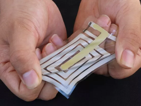
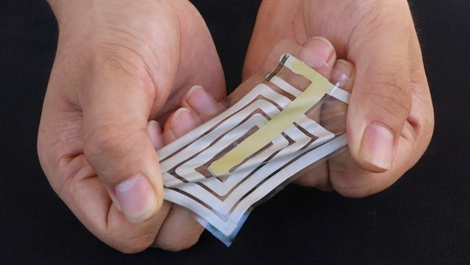
As the body’s largest organ, skin is responsible for the transduction of a vast amount of information. This conformable, stretchable, self-healable and biodegradable material simultaneously collects signals from external stimuli, which translates into information such as pressure, pain and temperature. The development of electronic materials, inspired by the complexity of this organ, offers a tremendous unrealized materials’ challenge. Fortunately, the advent of organic-based electronic materials may offer a solution to this longstanding problem.Zhenan Bao, K.K. Lee Professor of Chemical Engineering, Stanford University, is one of the world’s leading researchers working on the design of organic electronic materials that mimic skin functions. SEMI’s Maria Vetrano interviewed professor Bao to preview her February 25 keynote, Skin-Inspired Electronics, at FLEX|MEMS Sensors Technical Congress (MSTC) 2020, February 24-27, 2020, at the DoubleTree by Hilton in San Jose, California.Join us at FLEX|MSTC to meet Professor Bao and other industry influencers furthering innovation in flexible hybrid electronics (FHE) and MEMS sensors. Register now to connect with her at FLEX|MSTC or visit her on LinkedIn.SEMI: Your pioneering work on the use of electronic materials to construct second skin is a major step forward in human-machine interfaces. Could you please describe second skin?Bao: Second skin is a new electronic-device platform encompassing electronic devices that have skin-like properties such as stretchability, self‐healing ability, biocompatibility and biodegradability. In essence, the second skin is an electronic system of fully integrated multifunctional components operating on the surface of or inside the body to enable smart healthcare for disease prevention and treatment and to enhance the functional capabilities of natural skin. The second skin could also serve as a module to connect our human body to the Internet, thereby allowing human integration with the Internet of Things (IoT) for next‐generation wireless communications. In this way, we can view the second skin as an artificial body part that can be used to improve our everyday lives.SEMI: How might second skin operate in the human body?Bao: It has many potential uses. It could be a prosthesis for people who have lost their sense of touch. It could be used to repair damaged skin as well as to provide enhanced functionality that’s not possible with biological human skin. It could, for example, connect us with our external environment, with other people, even with our cars.I can also envision second skin as an implantable device for both neurostimulation and for early detection of disease. Schematic illustration of structure of second skin composed of functional devices: sensor, integrated circuit, display and power supply. Source: Stanford University SEMI: How did you get started in this research? Bao: Sixteen years ago when I started at Stanford, I learned of a colleague in mechanical engineering who was working on robotic cockroaches. That’s when I understood the need for sensor functions in robotics.I considered the large number of people with prosthetics who do not have a sense of touch. With this audience in mind, I started by designing a simple flexible electronic device that could take the shape of skin, even conforming to a robot hand, thereby approximating the natural sense of human touch.Once we developed the first sensor, and realized that its touch sensitivity could eclipse that of human touch, I asked myself: what can we learn from second skin – in addition to its sensing functionality?Skin is not just flexible; it is biodegradable and stretchable. So we started to dream. We began by developing electronic materials, either conductors or semiconductors. We added new functionality, such as self-healing properties, biodegradability and stretchability. That opened the way to new materials’ development.SEMI: What discoveries have you made in new materials?Bao: Over the past decade, we’ve developed skin-like materials with electronic properties that are on par with the best conducting and semiconducting polymers. Some of our skin-like semiconducting polymers can perform even better than amorphous silicon. That means with suitable processing methods, we can make stretchable ICs, initially with tens of transistors that can perform analog or digital functions, and in a later stage, stretchable displays driven by active matrix arrays.SEMI: What would it take to put these materials into production?Bao: We need to develop methods to pattern the skin-like electronic materials into fine features. We have been leveraging similar processes used for flexible circuit boards. Some research groups are developing roll-to-roll fabrication and printing methods.SEMI: Which technologies/applications are you commercializing?Bao: C3Nano is a Bao Research Group spin-off startup that is commercializing nanomaterials that are promising for bendable and foldable electronics.Another spin-off that is licensing our technology, PyrAmes, is developing a continuously non-invasive blood-pressure monitor. It’s not a cuff so the patient doesn’t have to remember to put it on.In the shorter term, we’re looking at putting artificial skin on prosthetic limbs and robotic hands. Further down the road, we could put skin on wounded regions of the body, forging connections to nerves that would support realistic sensation.To realize these applications, we’ll need to conduct further R D on materials and applications. The manufacturing of these devices still needs much more development.Fortunately, we’re part of a fertile development ecosystem at Stanford. I started the Stanford Wearable Electronics Initiative (eWEAR) to forge collaborations across Stanford campus as well as with industry.SEMI: What would you like FLEX|MSTC attendees to take away from your presentation?Bao: I’d like them to realize that the future of electronics is changing. I imagine a future in which the functions of a smartphone will disappear into what we wear, what we attach to our skin and what we implant inside our body. I believe that skin-like electronics will help to facilitate this future, allowing us to connect with each other and our surroundings in ways that feel natural, yet that also enhance our quality of life. Zhenan Bao is K.K. Lee Professor of Chemical Engineering with courtesy appointments in Chemistry and Material Science and Engineering at Stanford University. She founded the Stanford Wearable Electronics Initiate (eWEAR) and serves as the faculty director. Prior to joining Stanford in 2004, she was a Distinguished Member of Technical Staff at Bell Labs, Lucent Technologies from 1995 to 2004.Bao has over 500 refereed publications and over 65 U.S. patents with a Google Scholar H-Index 155. In her recent work, she has developed skin-inspired organic electronic materials, which have resulted in unprecedented performance or functions in medical devices, energy storage and environmental applications. She has pioneered several important design concepts for organic electronic materials. Her work has enabled flexible electronic circuits and displays.For more information on professor Bao’s research, visit Bao Research Group. FLEX|MSTC is organized MEMS Sensors Industry Group (MSIG) and FlexTech, SEMI technology communities focused on the growth of MEMS sensors and the flexible electronics supply chain, respectively. Maria Vetrano is a public relations consultant at SEMI.
Read More
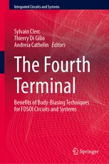
The chip design ecosystem finally has the book it’s been clamoring for: The Fourth Terminal - Benefits of Body-Biasing Techniques for FDSOI Circuits and Systems. [bctt tweet="The FD-SOI Chip Design Book: Yes, It’s Finally Here!" username="@soiconsortium"] The editors (who have also contributed chapters) are Andreia Cathelin, Sylvain Clerc and Thierry DiGilio, all world experts from STMicroelectronics. As Cathelin and Clerc note in the introduction: “The aim of this book is to introduce to the design community the straightforward design solutions in any modern FD-SOI planar CMOS technologies, by taking full advantage of body biasing techniques to efficiently modulate on the fly SoC solutions from high performance operation to energy efficiency mode. All design techniques are based on the classical pillar of regular planar CMOS devices. As the first fully industrial solution has been the 28nm FD-SOI CMOS technology from STMicroelectronics, all the design examples in this book have been demonstrated within this process integration frame.” [bctt tweet="The Fourth Terminal...taking full advantage of (FDSOI) body biasing techniques to efficiently modulate on the fly SoC solutions from high performance operation to energy efficiency mode" username="@soiconsortium"] The folks at ST were really the first to get into FD-SOI in a big way – in fact they’ve been at it for over two decades (!) so you’d be hard pressed to find experts at a company with deeper expertise. [caption id="attachment_29610" align="alignnone" width="535"] The Fourth Terminal team friends sporting Tour de Fourth Terminal t-shirts at ISSCC 2020. From left to right: MIT Prof. (and Series Editor for Springer's Integrated Circuits and Systems) Anantha Chandrakasan; Charles Glaser, Springer Editorial Director; Laurent Le Pailleur, ST; Andreia Cathelin, ST Fellow; Sylvain Clerc, ST; Stanford Prof. Boris Murmann (Photo courtesy Springer STMicroelectronics)[/caption] The Fourth Terminal is structured to cover three major areas: a technology overview (including body biasing for digital, analog and SRAM); a selection of circuits that illustrate body biasing in various fields; body bias deployment in mixed-signal and digital SoCs. The initial response has been tremendous. Editor Andreia Cathelin reports that posts she's made about it on LinkedIn were quickly viewed 10k times and more. Then came the book review by the eminent Stanford Professor Boris Murmann, who heralded its tour de force status in a clever turn of phrase: “With the help of a renowned international team of experts from industry and academia, the editors have distilled everything you need to know about FD-SOI circuit design into a 16-chapter "tour de fourth terminal". (Read his complete review here).[bctt tweet="Stanford Professor Boris Murmann calls this book a #Tour_de_Fourth_Terminal. #FDSOI #lowpower #chipdesign" username="@soiconsortium"] EETimes journalist Junko Yoshida blogged about it as Body Bias Gets Its Own Book (read that here), which generated lively discussions on LinkedIn (and underscored just how necessary this book is!). The Fourth Terminal - Benefits of Body-Biasing Techniques for FDSOI Circuits and Systems is part of the Springer Integrated Circuits Systems Series -- considered by many to be the most prestigious in the industry. Weighing in at 431 pages, The Fourth Terminal is available in both e-book and hardcover versions. See the Springer website to order this must-have addition to your library.
Read More