downloadGroupGroupnoun_press release_995423_000000 copyGroupnoun_Feed_96767_000000Group 19noun_pictures_1817522_000000Member company iconResource item iconStore item iconGroup 19Group 19noun_Photo_2085192_000000 Copynoun_presentation_2096081_000000Group 19Group Copy 7noun_webinar_692730_000000Path
Skip to main content
Default Banner Image

Technology and Trends

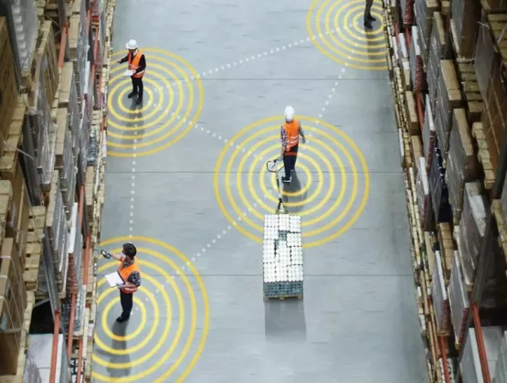
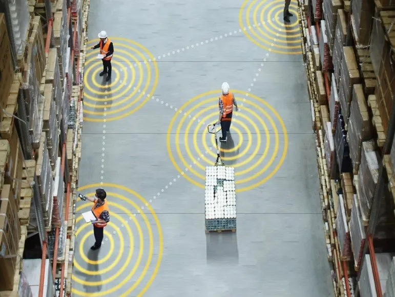
Earlier this year when the novel coronavirus, SARS-CoV-2, began sprinting around the world, public health officials told us that social distancing was the most effective way to slow its spread. We’re now many months into the pandemic, and social distancing, combined with mask-wearing, is still the best way to prevent new cases of the disease.On March 20, 2020, governors on opposite coasts, Gavin Newsom in California and Andrew Cuomo in New York, shut down their states, and other states soon followed. Only essential businesses, such as select retailers – grocery and hardware stores as well as pharmacies, for example – were allowed to remain open. Depending on location, however, it was days or weeks before strict social distancing measures were in place. Tape stuck six feet apart on store floors has helped shoppers keep their distance. But shouldn’t there be a more exact and reliable way to gauge social distances in retail stores, gyms, workplaces and other settings?David Horsley, founder and CTO of Chirp Microsystems, a TDK Group company, believes so, and the company is developing technology that does just that. Horsley will share the details in his keynote A Wearable Social Distancing Solution Based on Ultrasonic Time-of-Flight Sensors October 14 at MSEC 2020, SEMI’s first virtual MEMS Sensors Executive. The event is October 6-8 and 13-15, 2020. Register now for MSEC 2020.I spoke with Horsley to learn more about the sensors.SEMI: What was the inspiration for providing Chirp’s ultrasonic Time-of-Flight (ToF) sensors for social distancing?Horsley: Companies actually started contacting Chirp about six months ago to inquire about social distance tags to measure distance between people. They already knew about us because we’ve been supplying MEMS ultrasonic ToF sensors for virtual reality and robotics for several years, so they knew we could provide the same kind of low-power range-finding accuracy for resource-constrained devices. SEMI: How are your customers using Chirp-based social distance tags?Horsley: They’re designing Chirp’s ultrasonic ToF sensors into wearable tags worn by workers in distribution centers, in factories, and in oil and gas production, to name a few areas. The tags alert workers when they’re closer than two meters from another worker to ensure social distancing. Chirp’s ToF sensors also support contact tracing without recording any personal information, which is a major advantage over contact-tracing applications from companies like Google and Apple. Because those apps use Bluetooth Low Energy (BLE), which is already in your smartphone, the user has to enable location services. This records your GPS location, a privacy concern.BLE is problematic on some other levels as well. It only provides one-meter accuracy while Chirp’s ToF solution for social distancing delivers one-centimeter accuracy. Because BLE is only accurate within one meter, it can’t alert you in real-time that you’ve crossed that two-meter boundary to another person. Imagine you’re in the checkout line at the supermarket. BLE can tell you that other people are in your general vicinity, but it doesn’t have enough resolution to tell you whether the next shopper is two meters away from you or only one-and-a-half meters away. And because it doesn’t use the air as a medium, it registers a lot of false positives. If, for example, you’re separated from a person by a partition or a wall, and you’re within two or three meters of each other, your phone’s social-distance app will register a false positive.SEMI: Are you talking with customers in other environments, such as college campuses and theme parks?Horsley: There’s great deal of potential in those markets. For example, Professor Prabal Dutta’s group at UC Berkeley is working on a system that uses our sensors. His work also made us aware of some of the privacy concerns around contact tracing because universities are much more uneasy about student privacy than some private-sector companies are today. SEMI: What would you like MSEC attendees to take away from your presentation?Horsley: From the beginning, we believed that MEMS ultrasound was very versatile. We expected it to find a home in different types of applications because of its low power, small size and ease of use, particularly since we provide the enabling software that makes it all work. With design wins in four to five vertical markets, we’re experiencing significant marketplace validation. We’re all hoping that COVID-19 will wind down in the first half of 2021. As the focus on social distancing begins to fade, we’re looking forward to building out our customer base in the markets we’re in today as well as gearing up to explore new markets.Chirp Microsystems and TDK InvenSense are longtime members of MEMS Sensors Industry Group® (MSIG), a SEMI technology community that connects the MEMS and sensors supply network in established and emerging markets, enabling members to grow and prosper. Visit us today to learn how MSIG membership can make a difference in your business.David A. Horsley, Ph.D., is co-founder and CTO of Chirp Microsystems Inc., a TDK Group company. Horsley is also a professor of Mechanical and Aerospace Engineering at the University of California, Davis, and is adjunct professor of Mechanical Engineering at the University of California, Berkeley. Since 2004, he has been co-director of the Berkeley Sensor and Actuator Center (BSAC), the National Science Foundation’s Industrial/University Collaborative Research Center (I/UCRC) focused on MEMS research. Horsley is also a recipient of the National Science Foundation’s CAREER Award, and has authored or co-authored over 150 scientific papers and holds over 20 patents.Maria Vetrano is a public relations consultant for MSIG, a SEMI technology community.
Read More
While the world awaits a working vaccine to protect us from COVID-19, we need to employ all available tools to help curb the spread of this novel virus. On the one hand, it’s remarkable that we’re relying on the same low-tech tools that our forebears used to moderate the pandemic of 1918 — social isolation, mask-wearing and hand-washing. On the other, we have access to numerous technologies that hadn’t even been invented a century ago. Among the most important is molecular diagnostics for advanced testing.While we continue to face a scarcity of test kits in the U.S., the majority of commercially available genetic tests for COVID-19 are reliable, so accuracy is rarely the problem. We’re hampered instead by the timeliness of getting the results and by the level of detail the tests provide.To save more lives and reduce the burden on our healthcare system, we need point-of-care genetic tests that deliver accurate results rapidly, telling us right away who’s positive and who’s negative. We also need pertinent test data shared as quickly as possible via secure networks to improve our ability to track surges in infections. These are two of the challenges that emerging biotech companies are pivoting to embrace. RT-PCR: The Gold Standard in Accuracy, Not SpeedWhen I read about some of the high-quality COVID-19 tests on the market – such as Abbott’s, which detects positive results in as little as five minutes — I am awed by how far we’ve come since the last global pandemic. The core enabling technology in test platforms such as Abbott’s uses the molecular genetics technique real-time reverse polymerase chain reaction (RT-PCR). The vast majority of rapid tests administered today in hospitals and other clinical settings use RT-PCR.While accuracy is high for RT-PCR tests, getting tests results to patients is slow because test samples are sent to the lab for analysis. That lab could be located in a hospital, in a doctor’s office, or in an urgent care facility run by a large company such as Quest Diagnostics. Regardless of location, each lab must have an RT-PCR machine to read the test results. Plus each RT-PCR machine costs thousands of dollars, and requires a technician to read the results, , factors that have limited the proliferation of these machines.New COVID-19 cases are still surging in parts of the U.S., India and Brazil, and in some areas, we’re seeing instances of inundated labs, with test results coming back in one to two weeks. That’s not fast enough for a virus this contagious. We need to get accurate tests results to healthcare providers, public officials, and patients as close to real-time as possible. To meet this goal, we need to apply molecular-diagnostic techniques to new types of biosensors that deliver test results at the point of care in minutes through platforms that send that data in near real-time to the cloud. This essential information will allow public health institutions, states, cities and other key stakeholders to identify and mitigate emerging hot spots of disease.Over the past seven months, we’ve had the privilege of working with a handful of biotech companies that have pivoted to develop rapid point-of-care molecular diagnostics that target COVID-19. One of these, HEMEMICS, is developing a handheld molecular diagnostic test platform that could be administered by healthcare workers in triage settings such as ambulances, emergency rooms, community clinics and makeshift hospitals. As a true point-of-care test platform, it would deliver results onsite, without requiring the transfer of test samples to a lab. “We’re aiming to redefine point-of-care testing for COVID-19,” said John Lehman Warden, Jr., CEO and co-founder, HEMEMICS. “Unlike the most common type of on-site test — the lateral flow monitor — our test isn’t waiting for osmotic reactions to occur. We place the sample from a quick nasal swab or a drop of blood right on-chip, and binding takes place within a standing drop of fluid. That makes our platform fast, delivering results in about 60 seconds. Plus it simplifies sharing test results with other communities of interest, such as public health departments and municipalities, because it’s Bluetooth-enabled and supports cloud-based management networks.”As its foundry partner, we’re collaborating with HEMEMICS as it continues to refine its biochip’s sensitivity for both antibody and antigen testing of SARS-CoV-2. Once HEMEMICS is satisfied, it will move forward with the U.S. Food and Drug Administration’s (FDA’s) emergency use authorization (EUA), which it hopes will bring the HEMEMICS platform into the hands of the millions of people who stand to benefit.As we head into the fall and winter months, we’ll need both rapid, connected point-of-care biosensor test platforms such as HEMEMICS’ and high-accuracy RT-PCR tests to fight COVID-19 effectively. And at their root, we’ll have MEMS and biosensors to thank. For more information on Rogue Valley Microdevices’ biosensor solutions, please contact the company at [email protected] or visit its website. As founder and CEO of Rogue Valley Microdevices, Jessica Gomez has created a world-class precision MEMS foundry in the heart of Southern Oregon. Integral to her role as CEO, Gomez practices a business philosophy of offering best-in-class process technology and R D expertise to customers to help them achieve the highest quality and reliability in their products. Gomez plays an active leadership role within and beyond the technology industry. She is a board member of the prestigious SEMI Board of Industry Leaders, she was the first executive selected for Spotlight on SEMI Women, and she is chairman of the Oregon Institute of Technology Board of Trustees.Rogue Valley Microdevices is a longtime member of MEMS Sensors Industry Group (MSIG), a SEMI technology community that enables the MEMS and sensor industry to address common challenges, innovate and accelerate business results.
Read More
Even though microchips continue to get smarter, vital security gaps continue to be exposed through such hack attacks as Meltdown, Spectre, and in recent weeks, Plundervolt. Researchers continue to discover open doors in chip architectures for malicious players to steal increasingly sensitive data, hide the identity of counterfeits, or tamper with electronics systems most anywhere along the global microelectronics supply chain. Today, it’s impossible to have full visibility of the distributed chip making process – from design and fabrication to packaging, testing and delivery. That’s why our industry’s future hinges to a large degree on establishing a hardware root of trust throughout the silicon’s operational lifecycle. Trust but verify! It’s easy to say, but how do we do it?To gain insights, SEMI interviewed Dr. Mark Tehranipoor, currently the Intel Charles E. Young Preeminence Endowed Chair Professor in Cybersecurity at the University of Florida’s Electrical and Computer Engineering Department. A foremost authority on microelectronics security and trust, counterfeit electronics detection, and supply chain risk management, Dr. Tehranipoor will be a keynote speaker at the SEMICON Taiwan Security on Chip Summit, Friday, September 25, where a full program of industry leaders will address key security challenges and solutions involving IoT, systems on a chip (SoCs), integrated circuits, physical unclonable function (PUF) technology, future design, certifications, managed services, and more.For additional insights and to hear Dr. Tehranipoor’s full presentation, register for SEMICON Taiwan 2020, which SEMI is holding as a hybrid event with both a virtual format and an in-show program September 23-25.SEMI: What are the major uncertainties in providing the hardware root of trust within the cyber domain?Tehranipoor: One of the most critical issues we’re dealing with now is loss of control over the process of designing and fabricating integrated circuits and systems. This has happened along with globalization and the movement of supply chain operations overseas to lower costs of nearly all goods, including electronics products and semiconductors. As skill sets, talent, design and fabrication have all shifted offshore, concerns have also risen about security controls across the many different segments of the microelectronics supply chain.For example, when you think about the security of military, space, transportation, power grids, financial or other networks, it becomes a major concern if you cannot trust the underlying electronics system that runs them. New SoCs are also holding more sensitive data around encryption keys, biometrics, personal information or banking data. And as reports escalate about cybersecurity gaps at the electronics part level, it’s increasingly important to establish a hardware root of trust. Today, it’s not enough for a buyer to just call up the design house and verify the electronic ID of an asset. The ID might match, but the device could have been tampered with or replaced with a counterfeit somewhere along its end-to-end journey. Unlike software or networks where problems can be automatically identified, upgraded and fixed, verifying electronic hardware is a costly and time-consuming process, especially when they’re as complex as microchips. It can take months to deconstruct, reverse engineer, inspect, and authenticate a chip. By then, discovery of any security breaches is too late.When addressing the security of electronics systems, there are three important features to keep in mind. First, there’s confidentiality. The device shouldn’t leak information to an unauthorized user. Second, there’s integrity. Unauthorized users should not be able to manipulate an SoC’s sensitive data. The third feature is availability, which can be a result of Denial of Service (DoS) attacks. If the device is under attack and can’t access your online service or network, you must still have security measures for your electronics system to be available in a safe mode while you simultaneously identify the problem, recover from it, and return to normal functions.SEMI: What framework should be followed to establish greater trust and confidence across the entire microelectronics supply chain?Tehranipoor: In the United States, we recognize it may not be possible to bring all manufacturing, design, and delivery teams back to this country and have them certified by the U.S. Department of Defense. You could do some of it, but it would be very costly and complex to bring back all the design, fab, testing, and packaging operations involved with electronics systems and still have complete control.The most practical approach is to make sure we design electronic systems with security and trust in mind from the start. We need to provide security features up front throughout the extended supply chain – into the design flow, fab flow, and out into the field to make it easier and faster for anyone at any point to verify the authenticity of an electronic system as well as identify and mitigate a problem. Finally, we have to remember that we are all in this together – designers, developers, packaging facilities and fabs. We can’t just blame semiconductor manufacturers or any other single entity. As a result, we must be cooperative and collaborative by focusing on this issue as a consortium. Everyone in this ecosystem must come to the table, share best practices, establish standards, and initiate best practices for device to system authentication.SEMI: How can SEMI and the SEMI Electronic System Design (ESD) Alliance help the industry meet these challenges?Tehranipoor: It’s certainly of utmost importance for members of organizations like SEMI and its ESD Alliance committees to jointly develop and adhere to standards or guidelines that establish hardware root of trust across all participants in the global supply chain. At the same time, such alliances should make it a high priority to protect each company’s intellectual property (IP). Collectively, we need resolutions that allow us to develop unique IPs and more easily trace, identify, and verify the authenticity of electronics systems as they flow throughout the end-to-end electronic supply chain. Great efforts are under way and progress is being made. But it’s not enough. Clearly, more needs to be done to establish root of trust standards at the chip level.I can’t emphasize enough the importance of consortia like the SEMI ESD Alliance to create an environment where industry, government, and academia can come together, share best practices and even case studies on how they handled security vulnerabilities and breaches. We understand that not everyone wants to share their security problems, vulnerabilities, or attack surfaces, but learning from each other’s experiences can have a tremendous impact on industrywide progress. If you don’t know what you need to address, you won’t be able to address it when it happens.I also encourage organizations like SEMI to create standards or guidelines that reduce the complexity of microchip designs for security purposes. Realtors often say there are three things to consider in finding a home that will appreciate in value: Location, location, location. To build more secure electronics systems, my mantra is: Automation, automation, automation. Complexity is the enemy of security. By using automation to simplify security mechanisms and detect inconsistencies, it will be easier to find and fix security problems, not to mention lower costs at the same time. SEMI: What will an attendee take away from your talk at SEMICON Taiwan?Tehranipoor: I have a large team of researchers who day and night spot vulnerabilities by attacking and assessing data from different electronic systems set up in our labs. Attendees will see real-world examples and lab animations that show how electronics systems can be hacked most anywhere across the supply chain. They will also learn about step-by-step security solutions we have developed at the microchip level. We need to do a better job of protecting the security of our semiconductor assets and the electronic solutions or services they power. My call to action will be that we need to invest more in research and foster an environment of more open trust and cooperation. We can do this by bringing together different countries, companies, and organizations in the microelectronics ecosystem to overcome this major challenge.Dr. Mark Tehranipoor is currently the Intel Charles E. Young Preeminence Endowed Chair Professor in Cybersecurity at the ECE Department, University of Florida. He is currently serving as Director for Florida Institute for Cybersecurity Research (FICS), National Microelectronics Security Training Center (MEST), CYAN Center of Excellence, and ECI Transition Center. He also serves as Program Director of Cybersecurity for UF Herbert Wertheim College of Engineering. His current research interests include IoT security, hardware security and trust, and reliable circuit design.Samer Bahou is senior manager of corporate communications at SEMI.
Read More
Teck Khiong, WOI, senior manager of Factory Integration at Infineon Technologies Asia Pacific Pte Ltd, recently shared with me how the Infineon backend plant in Singapore has benefited from its journey to qualify for the lighthouse certification.WOI is driving Infinion smart manufacturing projects with a strong focus in the area of connect and control using IoT (Internet of Things) and analytics technologies. Ng: How did the Infineon backend plant in Singapore distinguish itself to qualify for lighthouse certification? WOI: The Infineon Singapore backend manufacturing plant is proud to be a Lighthouse Certified Smart Manufacturing site as part of the World Economic Forum’s (WEF) Fourth Industrial Revolution platform. Our Industry 4.0 (I4.0) implementation reduces labor costs by 30% and improves capital efficiency by 15%. We drove this successful digital transformation continuously investing in our people development and digital backbone.Of the many initiatives under our I4.0 Smart Factory platform, five were selected for WEF Lighthouse submission and certification. Digital foundation with integrated connectivity and workflow execution We implemented an Internet of Things (IoT) framework to connect machines to manufacturing system more than two years ago. The digitization of our Work-in-Progress (WIP) management systems provides full traceability and gives us better control of the four Ms (Man-Machine-Method-Material). Material handling and process automation We progressively deployed automated solutions starting six years ago using autonomous transport, robotic material management systems and automation of packing processes. This eliminated non-value touches in areas of WIP storage and retrieval. Advanced algorithms enabled WIP scheduling and dispatching As our product mix and volume grew in complexity, our advanced algorithms has enabled us to increase our machine uptime, thus reducing idle and set-up time. Manufacturing control tower Our control tower provides a real-time pulse of the entire manufacturing process, from machine efficiency to quality. The tower also improves data integrity and collaborative information sharing while issuing early-warning alerts that enable exception management and timely decisions. Running a global virtual factory Our Global Production Network deployments allows us to connect and manage a growing contract-manufacturing network in real time, with the same transparency, traceability and control as if the manufacturers are our internal sites.About Teck Khiong, WOITeck Khiong, WOI graduated from Loughborough University in the UK with a Master of Science degree in Computer Integrated Manufacturing (CIM). For more than 20 years he has delivered manufacturing IT solutions to global backend (assembly and test) semiconductor manufacturing, ranging from equipment, factory, process control, material handling automation and manufacturing execution systems (MES).
Read More
If you bought a new car recently, you must have noticed that it warns you if one of its functions needs your attention. It even alerts the factory if repairs or major adjustments are needed. Wouldn’t it be nice to have similar capabilities for our bodies that will call for a “service” before we end up in an emergency room – or worse? The United States invests almost 18 percent of its Gross Domestic Product (GDP) in healthcare. Such a significant part of our economy deserves our industry’s attention – and it gets it. SEMI’s recent Smart MedTech webinar series tells not only patients and healthcare providers how electronic products can impact their lives, but also offers device makers plenty of ideas for developing new solutions.SEMI Gets SmartIn addition to working on many important topics with more than 2,200 member companies across the semiconductor supply chain, SEMI focuses on special areas: Smart Mobility (as covered here), Smart MedTech (covered below), Smart Manufacturing, and Smart Data. Smart MedTech was the topic of four recent webinars, organized by Melissa Grupen-Shemansky, executive director Nano-Bio Materials Consortium (NBMC), and Chief Technology Officer, SEMI. NBMC’s mission is to enable flexible, wearable human performance monitoring. In her introduction, she emphasized that healthcare will shift from today’s provider-centric approach to a personalized care model, with the following characteristics: Outcome-based Decentralized, not limited to geographies Specific to your personal health and medical needs With a team of providers, connected like never before To achieve all these characteristics, microelectronics will be an essential contributor. That is why SEMI and member companies are working on platforms to fund and commercialize R D as well as to educate potential users and beneficiaries. Grupen-Shemansky engaged a series of experts and organized four webinars to address this broad and complex field, and outline their contributions to meeting the above criteria. They have been recorded and are available to SEMI members. Call your SEMI contacts to find out where and how you can access slides and recordings of more than a dozen presentations.From Biomarkers to BioChemical Sensors Physiological RelevancyTo monitor a human body’s performance, researchers have to first understand which biomarkers indicate specific conditions of the body, then learn how to capture and process the data. Grupen-Shemansky moderated this August 5th session. Christina Davis from UC Davis, Jennifer Martin, and Sean Harshman from the Air Force Research Lab (AFRL), and Kenneth Ward from Pacific Diabetes Technologies presented their ongoing efforts in this field.Davis talked about the challenges of analyzing exhaled breath, which contains 99% water and 1% biomarkers. She showed a hand-held analyzer her team has developed (Figure 1). She also elaborated on how to interpret the captured data and, if needed, decide which follow-up treatments are advised.Figure 1: Palm-sized µCON exhaled breath micro-condenser used to analyze biomarkers. (Courtesy: UC Davis) AFRL’s Martin and Harshman outlined how ongoing and future minimally invasive techniques are being used to monitor airmen, and give them advice for self-treatment to maximize their performance. The Pacific Diabetes Technologies speaker, Ward, showed how to use minimally invasive, subcutaneous (=under the skin) oxygen sensors to detect hemorrhage (= blood loss) and control it.En Route Care (ERC) and Point of Care (POC) DiagnosticsTreating injuries right away and correctly shortens not only a patient’s suffering, but also improves his or her chances for a full recovery. AFRL’s Matthew Dalton moderated this August 12th session. Derek M. Sorensen from AFRL, Zheng Yan from the University of Missouri-Columbia, Melinda Eaton from the Virtual Health Program Management Office at the U.S. Department of Defense (DoD), and Azar Alizadeh from General Electric (GE) Research outlined their contributions to achieving instant and professional care.AFRL’s Sorensen described the many challenges a Critical Care Air Transport Team (CCATT) deals with when performing their work inside a noisy, dark, hot, or cold, shaking airplane, discussed their equipment and personnel constraints, and explained how difficult it is, even for experienced doctors, to perform emergency surgeries under these conditions.Professor Yan takes low cost very seriously and demonstrated how he and his students have developed on-skin wearable sensors that can be manufactured by using only pencil and paper.Eaton outlined the DoD’s strategy for assuring its medical force is ready to support soldiers. Then she discussed a broad range of the DoD’s traditional health management responsibilities and added that Covid-19 is now an important factor.Alizadeh addressed how GE microelectronic solutions improve the efficiency of care, reduce medical errors and length of hospital stays as well as improve workflows of caregivers. In addition to GE’s well-known, large/stationary medical equipment and communications infrastructure (Figure 2), Alizadeh showed that GE is also providing skin patches and other wearable sensors to capture data.Figure 2: The Future of Monitoring: In 2017, Mercy Hospital served 800,000 patients with telemedicine including those with chronic diseases. Patient:doctor ratio: US average 300:1. Mercy = 1100:1. (Courtesy: GE) Human Wearables Enabling Rapid Decision Making in the Integrated Care ContinuumAs Figure 2 above shows, microelectronic equipment can improve patient care and efficiency of medical personnel, but only if sufficient data can be captured timely and accurately – increasing the importance of wearables. AFRL’s Jeremy Ward moderated this August 17th session. Christopher Scully from the U.S. Food and Drug Administration (FDA), Ashleigh Coker from the AFRL’s Sensors Directorate, Ted Harmer from the AFRL’s Airman Systems Directorate, and AFRL’s Regina Shia presented for Oxana Pantchenko from NextFlex how they develop wearables jointly. Scully introduced the FDA’s organization and its responsibilities, described the high-value accurate data can provide, warned about the damage false alarms and equipment failures can cause, and explained the regulatory role the FDA plays in this context.AFRL’s Coker highlighted the essential role sensors play in modern warfare with several examples, described her directorate’s operations and showed their warfighter-centric design process (Figure 3).Figure 3: Warfighter-centric design process steps and the need to engage multiple heads/perspectives in this process. (Courtesy of AFRL) AFRL’s Harmer addressed the importance of good communications architecture and protocols to capture and compute data to assure efficient cooperation between land/air/sea/space-based forces.NextFlex’ Pantchenko prepared a presentation about standards-compliant wearable electroencephalography (EEG), electromyography (EMG), and electrooculography (EOG) devices, jointly developed with AFRL and several other companies. It was delivered by AFRL’s Regina Shia.Automation, Augmentation and AINatalie Wisniewski, Founder of Profusa, Inc. a and consultant in Wearables and Digital Health, moderated the fourth webinar, held on August 26. She emphasized SEMI’s role in this context, then introduced the speakers: Michael Kirby from Colorado State University, Kevin Zhao from Harmonize Health, Mary Clare McCorry from armi/biofab USA, and Andreas Caduff from ETH Zuerich.Professor Kirby outlined several mathematical principles that need to be applied to get meaningful results when analyzing data. He emphasized that genetic factors influence if an individual is susceptible, tolerant, or even resistant to certain pathogens and warned that bacteria can develop resistance to today’s antibiotics.Zhao from Harmonize talked about the importance of predictive analytics in remote care, how to filter out false alarms, and how to deliver the best available care cost-effectively. In closing, he emphasized that computers and algorithms are not replacing clinical staff.McCorry outlined how biofab USA, a program of armi, uses sensors and automation to grow replacement tissue and organs (Figure 4). She explained how they use engineering principles and life sciences to make guide cells grow into replacement tissue. The company’s plan is to expand the currently lab-based capabilities into an industrial scale tissue foundry.Figure 4: Growing ear cartilage in the lab. (Courtesy: armi/biolab USA) SummaryMcCorry summarized her presentation, and actually the entire webinar series, with these statements: The human body is a 3D, highly complex, dynamic, and multi-faceted biological construct Skin lends itself well as an interface between body and wearable sensors Connecting physiology (e.g. vital signs), behavior, and external factors is important for getting good results Verification, validation, and FDA involvement are important for making methods and devices successful Sensors, communication computing (AI/ML) are complementing, not replacing, medical personnel Today’s methods and devices will be outperformed by tomorrow’s solutions – stay up to date Personal CommentsSummarizing eight hours of presentations in a few pages requires a very high and lossy compression factor – please understand. I suggest you call on your SEMI contact to get access to these previous and following webinar recordings. Excellent contacts across the electronics supply chain enable SEMI to win experts in many areas to convey valuable information in these webinars.I am impressed that the USA military, specifically the AFRL, invests so much effort in medical support for airmen/women. They demonstrate that only healthy and fit personnel can take full advantage of the sophisticated weapon systems at their disposal if/when they are called upon to deploy them.This Smart MedTech webinar series confirms what many medical experts told me during exams and/or before and after surgeries: The human body is a masterpiece of bioengineering. These webinars also reminded me of what I learned at a brain-health class at Stanford University: Our brains only need about 20 Watts to perform computing and memory tasks that fairly quickly approximate the results of today’s computers – a benchmark for computer architects and AI/ML experts.Republished with permission from 3D InCites.
Read More
Making Strides TogetherKnowledge is power – especially when it is shared. This principle formed the foundation for Micron’s Go and See virtual visit of its Singapore manufacturing plant on 26 August 2020 as 27 companies including GLOBALFOUNDRIES, ST Microelectronics, Infineon, TEL, ViTrox , IBM, HP and UTAC joined the first-of-a-kind virtual factory visit. The chip industry powerhouses gathered to see how Micron’s Lighthouse frontend wafer fabrication facility leverages Fourth Industrial Revolution technologies to drive new production and cost efficiencies.They saw clear markers of a transformed organisation and spoke with working-level staff, managers and front-line employees. Company representatives also met virtually with Micron management teams from organisations that led its digital transformation – from pilot programs to integration at scale – to realise significant financial and operational benefits. The mix of technologies they deployed to make it all happen included artificial intelligence (AI), big data analytics and the Industrial Internet-of-Things (IIoT).Micron’s Singapore-based fab facility earned Lighthouse certification earlier this year from the World Economic Forum’s Global Lighthouse Network. The Go and See tour was co-sponsored by SEMI Southeast Asia and McKinsey Company.Transformation is CrucialBy embracing Lighthouse principles, semiconductor sectors and companies can accelerate their digital transformation to boost operational and financial efficiency while helping increase productivity across the electronics supply chain. It will take time for Southeast Asia semiconductor manufacturers to transform to digital operations, though we’re seeing growing interest in Industry 4.0 practices as they begin to understand that the deployment of new technologies and applications will help them better understand real-world benefits of smart manufacturing use cases and solutions. SEMI believes shining the spotlight on companies like Micron can illuminate the way forward for other companies to help drive the industry’s digital transformation. We look forward to seeing companies build on this momentum as they start to leverage leading-edge technologies to improve efficiencies and promote sustainability.Bee Bee Ng is president of SEMI Southeast Asia.
Read More
About 70% of the U.S. Gross Domestic Product (GDP) is driven by consumer demand. What consumers are looking for is influenced by, for example, fashion trends, product innovations, environmental forces, and personal interests. Regarding personal interests: Sales of electronic components at Fry’s are poor. Radio Shack stores even vanished completely. Today’s consumers do not like to tinker; they want to buy software-enabled, user-friendly systems with over-the-air updating that serves their current and future requirements well – e.g. smartphones. System vendors followed the same transition, and so did semiconductor vendors. Instead of offering (low margin) components, they develop and manufacture big portions of, if not complete, (high value) hardware and software solutions for electronic systems, targeted at specific markets.Mid-August, two SEMI webinars outlined the Smart Mobility market and what it expects from system and semiconductor vendors.SEMI's Smart Initiative“None of us knows as much as all of us,” “Connect – Collaborate – Innovate,” and other strategic considerations have motivated SEMI to become the gateway for the $2 Trillion (= 2,000 Billion) global electronic design and manufacturing supply chain. Figure 1 shows how many companies and organizations have joined this large industry organization, to work together efficiently and serve customer demands cost-effectively. Especially in four high-growth markets/application areas – Smart Data, Smart Mobility, Smart MedTech, and Smart Manufacturing – SEMI enables highly rewarding cooperation. Figure 1: Overview of SEMI members, technology communities, and areas of focus. (Courtesy: SEMI) MEMS and Sensors for Smart Mobility Tim Brosnihan, executive director of MEMS Sensor Industry Group (MSIG), moderated the webinar on MEMS and sensors for Smart Mobility. Bettina Weiss, Chief of Staff and Global Smart Mobility Lead at SEMI, presented the overview. In addition to Figure 1 above, she showed how many companies are now supporting SEMI’s Smart Mobility efforts and have joined the Global Automotive Advisory Council (GAAC). The European GAAC was founded in 2018, based on requests from VW and Audi. Regional chapters have also been formed in the U.S., China, Taiwan, and Japan. Figure 2 shows the current members of the American GAAC – new members are welcomed in all five regions. Figure 2: Current GAAC members in the Americas. (Courtesy: SEMI) Market Trends and Technology Innovations in MEMS Sensors Andreas Breiter, Partner at McKinsey Company, addressed markets, and Armen Mkrtchyan, Associate Partner at McKinsey Company, spoke about technology. Breiter addressed both vehicle and infrastructure changes required, as well as many ongoing and planned activities to enable Smart Mobility. He outlined autonomy, connectivity, electrification, and shared mobility of vehicles as the major opportunities for MEMS sensors. Mkrtchyan showed which technologies enable Smart Mobility and which regions will invest how much in software, hardware, and services by 2030, to capture data and process it in partially/fully autonomous vehicles’ Domain Control Units (DCUs) – see Figure 3. Figure 3: Pre-COVID market estimates. (Courtesy: McKinsey Company) MEMS-based sensors are used in vehicles to monitor pressures and perform as accelerometers or gyroscopes. Non-MEMS-based sensors capture light (e.g. for time-of-flight distance measurements) or magnetic fields (e.g. for RPM measurements). Regarding the many infrastructure upgrades needed for enabling autonomous vehicles on the roads, in Figure 4, Breiter gives road planners a lot of food for thought and planning work. City planners face much more complex challenges. That’s why electronic systems will also be needed to make these large infrastructure investments earn returns. Figure 4: Smart roads are essential for autonomous driving. (Courtesy: McKinsey Company) EDA and Smart Mobility The second Smart Mobility webinar focused on how Electronic Design Automation (EDA) tool vendors, Intellectual Property (IP, System Building Blocks) vendors, and system/IC Design Services can contribute to the success of Smart Mobility. Bob Smith, executive director of Electronic System Design Alliance (ESDA), moderated the webinar, highlighting where the relatively small but essential ESDA and its members fit in the semiconductor ecosystem – see Figure 5. Figure 5: EDA, IP, and design services enable the entire electronics ecosystem. (Courtesy: ESDA) Bettina Weiss explained how SEMI and the Smart Mobility Team are working to bring together stakeholders in the semiconductor ecosystem in general and the Smart Mobility segment specifically, to jointly address topics of common interest, work on solutions and agree upon standards where and when needed. Market Trends and Technology Innovations in EDA, IP and Design Services Andreas Breiter and Armen Mkrtchyan presented McKinsey’s perspectives regarding these topics. In addition to the above-mentioned market data, Breiter emphasized that DCUs are playing an increasingly important role in capturing the data provided by smart sensors, are processing it, and initiating appropriate actions. Together with application-specific software, these DCUs perform tasks like sensor fusion, manage creature comfort, assure safe operation of the vehicle, and secure communication with the outside world (Figure 6). Figure 6: High growth for DCU; likely shift in business models. (Courtesy: McKinsey Company) Mkrtchyan addressed EDA, IP, and services for Smart Mobility from 10 different technical perspectives. Here are the highlights. Component failures can and will have severe consequences in Smart Mobility. Therefore screening, testing, and exhaustive verification are extremely important. Software content is likely to increase at 10% CAGR during this decade. To increase the productivity of software and middleware developers, he emphasized that standards need to be agreed upon. Over-the-air (OTA) updating capabilities are needed. That’s why cybersecurity is important to keep vehicles current and safe. Power train electronics need to function at up to 150°C. New materials will be needed to increase reliability, reduce cooling efforts, and lower unit costs. Last, but not least, Mkrtchyan emphasized that every city needs to design its own infrastructure, not only to enable Smart Mobility but also to monetize the large investments needed; EDA, IP and design support will help to achieve both. In summary, he stated that Design and IP as well as packaging and test will be the most impacted areas in the transition to Smart Mobility. Personal Comments After having attended several MSIG events, I am impressed by how MEMS, NEMS (Nano…), and sensors can lend machines in many ways sight, smell, taste, touch, and hearing. They can replicate these human senses, often better than found in us. If you, like me, celebrated when your first modem enabled your PC to communicate with the entire world, you’ll appreciate the value MEMS and sensors can and will add to machines’ “communication skills.” Also, I can assure you that innovative engineers in this field will find many new ways to capture data in the physical, chemical, and biological domains and enable machines to keep humans safe. (I look forward to a handheld Covid-19 sensor that provides results within a few seconds!) Having worked for a small, then a large EDA vendor, many years ago, and for the ESD Alliance several years ago, I know how difficult it is to motivate innovative software developers to work together or agree upon standards. I am glad that the ESD Alliance is now working closely with SEMI. Most SEMI member companies, and their innovative employees, have learned over the years how important standards are to reduce development cost, processing, and test time, as well as time to profit. I wish Bob Smith and the ESDA members all the best for cooperating closely to define design standards, bi-directional hand-off points up and down the entire supply chain, primarily at the interface between design and manufacturing. I want to encourage EDA and IP experts to work closely with the experienced and knowledgeable people in materials, equipment, manufacturing, and test. 5G mm-wave communication, artificial intelligence/machine learning (AI/ML), reliable solutions for Smart Mobility, and development/characterization of new materials offer great opportunities and challenges for design AND manufacturing. Together, these two big camps can monetize required solutions much better and faster, than on their own. Your contact at SEMI can tell you how and where you can watch the webinar recordings and/or download all the slides. P.S.: Having two eCars and one eBike in our garage encourages me to appreciate SEMI’s efforts in advance Smart Mobility! Republished with permission from 3D InCites.

Read More