downloadGroupGroupnoun_press release_995423_000000 copyGroupnoun_Feed_96767_000000Group 19noun_pictures_1817522_000000Member company iconResource item iconStore item iconGroup 19Group 19noun_Photo_2085192_000000 Copynoun_presentation_2096081_000000Group 19Group Copy 7noun_webinar_692730_000000Path
Skip to main content
Default Banner Image

United States

United States AI Techniques in Semiconductor MFG Business Executive Technical

Suggested Hotels:

Embassy Suites by Hilton Milpitas Silicon Valley

901 East Calaveras Boulevard

Milpitas, CA 95035

(408) 942-0400


Courtyard by Marriott Milpitas Silicon Valley

1480 Falcon Dr.

Milpitas, CA 95035

(408) 719-1966


Event Sponsors

Sponsorship Opportunities

Enhance your brand with our exclusive sponsorship packages. For details, contact:

Karim Somani
Email: [email protected]

Highlighted content

SEMI HQ
673 S Milpitas Blvd.
Milpitas, CA 95035
United States

Morning, Day 1: August 5th, 2026

9:00 am - 10:30 am
Surya Kalidindi
Multiscale

Emergent AI/ML Tools for Semiconductor Manufacturing Technology Optimization

Semiconductor manufacturing faces a broad set of complex challenges addressed through Yield Management Systems (YMS), Fault Detection and Classification (FDC), Run-to-Run (R2R) control, Design of Experiments (DOE), and Statistical Process Control (SPC). Existing machine learning approaches are predominantly scoped to individual process steps or short loops, leaving full-traveler analysis — essential for informed tool decisions such as hold, parameter adjustment, and recipe modification — largely unaddressed. Bespoke, step-specific models do not generalize across process nodes or design variants, and manually configuring analytical workflows for each new use case is time-intensive and error-prone as technology nodes diversify. General-purpose coding agents built on large language models (LLMs) partially close this gap by automating workflow generation, but they lack the semiconductor-specific domain knowledge required for robust, production-grade solutions: open-source ML packages carry no fab context, and proprietary data curation and signal-processing conventions are rarely captured in public training corpora.

This session shows how a fab-aware agentic approach closes that gap, focusing on three use cases: YMS, FDC, and Process DOE. It opens with a technical primer built on a common pipeline — preprocessing and feature reduction, uncertainty-aware imputation, regime-aware modeling (physics and virtual-metrology priors when data is scarce, data-driven as it grows), and interpretable attribution rather than black-box scores — instantiated differently across the three, with emphasis throughout on when a result can be trusted. YMS downselects high-dimensional metrology, imputes sparse measurements, and trains a tuned regressor ensemble (GPR, gradient-boosted trees, neural nets), with feature attribution (SHAP) mapped to process step and tool. FDC aligns traces, then layers univariate control limits (SPC) with multivariate anomaly detection (PCA, Hotelling T², MEWMA), per-sensor attribution, and alarm-budgeted limits that transfer across chambers. Process DOE designs experiments, fits uncertainty-aware surrogates (Gaussian processes), reduces dimensionality (PCA), and selects runs sequentially (single- and multi-objective Bayesian optimization). Attendees then see these techniques operationalized live by a domain-specific agentic platform and work directly with the agents on curated datasets.

By the end, attendees will understand how problem formulation, data characteristics, and method selection shape outcomes, and what distinguishes a domain-aware agentic workflow from a general-purpose coding agent. The session is interactive by design — participant choices steer the live analysis, and attendee input shapes how these capabilities evolve.

10:30 am - 11:00 am
Maryia Kurdina
AI R&D Group Leader
TEL and AI Design (TTAD)

Real-Time Equipment Health Monitoring Using Gaussian Process Regression on Sensor Signals

Will present a real-time health monitoring method for semiconductor equipment using multi-sensor time-series signals. From a small set of baseline runs (typically 5–20), Gaussian Process Regression is used to learn expected sensor behavior and associated confidence bands over repeatable operating segments. At runtime, deviations from these bands are aggregated into health scores per sensor and segment to identify abnormal behavior early. The system automatically reports anomalies and raises warnings to support proactive maintenance and reduce unplanned downtime and quality risk. To address the O(N^3) training cost of standard GPR, we use a split-training approach that achieves linear scaling, keeping computation practical for production use.​

11:00 am - 11:20 am

Break

11:20 am - 12:20 pm
Viraj Modak, Aditi Gautam, Saira Qureshi
Nvidia

Predict Before Failure: A Predictive Maintenance Blueprint with NV-Tesseract and NeMoClaw

Semiconductor fabs generate high-volume, multivariate sensor telemetry from process tools, ambient monitoring systems, sub-fab equipment, etc. Scheduling maintenance operations depends on more than just reacting to alarms/alerts: teams need to forecast how equipment will behave and detect abnormal trajectories/baseline shifts before failures occur.​
​
This session introduces an open Predictive Maintenance Blueprint that embeds NV-Tesseract as the core time series AI component. The pipeline performs multivariate forecasting on equipment sensor data, then runs diffusion-based anomaly detection on the forecasted window to flag emerging degradation patterns. ​

The blueprint is packaged as a reusable, deployable workflow with Hugging Face weight retrieval, configurable sensor channels, and structured outputs for downstream automation.​

We extend this blueprint with NVIDIA NeMoClaw, treating predictive maintenance as an always-on agent workflow: an autonomous agent ingests sensor streams, invokes the NV-Tesseract pipeline, interprets anomaly scores, and produces operator-ready summaries and recommended actions under OpenShell runtime guardrails. ​

Together, this shows how foundational time series models and agent orchestration can be coupled to build a production-style Predictive Maintenance stack for semiconductor operations.​

What the Audience Will Learn​:
Predictive maintenance is shifting from threshold-based SCADA alarms to forecast-then-detect workflows that catch drift earlier on multivariate equipment signatures.​

Foundational time series models (like NV-Tesseract) are increasingly deployed as components inside larger agent systems, not as standalone notebooks.​

Semiconductor and industrial teams are adopting blueprint + agent patterns (similar to NeMoClaw deployments in EDA, simulation, and factory ops) to move from prototype to governed, repeatable workflows.​

Practical lessons: multivariate sensor alignment matters; model weights and configs should be versioned and auto-retrieved; anomaly outputs must be explainable enough for maintenance engineers to trust and act on.​

Architecture takeaways:​
When to use multivariate forecasting vs. single-signal monitoring.​

Why diffusion-based anomaly detection fits correlated, high-dimensional fab sensor data better than univariate reconstruction approaches.​

How NeMoClaw can orchestrate the pipeline: data ingest → inference → thresholding → alert routing → human-in-the-loop review.

12:20 pm - 1:30 pm

Lunch

1:30 pm - 2:00 pm
Sean Tropsa & Kyle Clark
SEEQ

Practical Agentic AI at Scale for Manufacturing: Lessons Learned from Large-Scale Deployments​

Agentic AI is nearing mainstream adoption, yet many organizations still lack a clear strategy for deployments at scale. In order to bring LLM capabilities to manufacturing, companies need to go beyond what mainstream AI suppliers can deliver; they need AI deployments to be governed, reliable, repeatable, and scalable enough to earn trust and deliver measurable results. Most importantly, it must be grounded in and continuously integrate the knowledge of subject matter experts who understand the complexity of real systems and processes.​

​
In this session, we will share lessons learned from deploying large-scale agentic AI solutions in the semiconductor industry. We will explore how SME expertise and operational context can be embedded into Agentic AI systems to create trusted, high-value results. Specifically, we will show how an auto-Triage/RCA a Facilities Anomaly event workflow can be set up such that, as the event triggers, an AI agents completes a first pass investigation that is ready for consumption by the end user shortly after an event triggers with an optional integration with CMMS systems to ease the creation of a work order to drive faster time to resolution and greater consistency in event disposition. We will also demonstrate how engineers can build custom apps and AI agents on demand, without requiring an AI specialist or extensive coding skills, while maintaining the structure and scalability needed for enterprise adoption. Attendees will leave with practical insights for enabling better, faster decisions across engineering, technician, and operator workflows.

Afternoon, Day 1: August 5th, 2026

2:00 pm - 3:00 pm
Steven Sheets
Lam Research

Human-Machine Collaboration for Improving Semiconductor Process Development

One of the bottlenecks to building semiconductor chips is the increasing cost required to develop chemical plasma processes that form the transistors and memory storage cells1,2. These processes are still developed manually using highly trained engineers searching for a combination of tool parameters that produces an acceptable result on the silicon wafer3. The challenge for computer algorithms is the availability of limited experimental data owing to the high cost of acquisition, making it difficult to form a predictive model with accuracy to the atomic scale. Here we study Bayesian optimization algorithms to investigate how artificial intelligence (AI) might decrease the cost of developing complex semiconductor chip processes. In particular, we create a controlled virtual process game to systematically benchmark the performance of humans and computers for the design of a semiconductor fabrication process. We find that human engineers excel in the early stages of development, whereas the algorithms are far more cost-efficient near the tight tolerances of the target. Furthermore, we show that a strategy using both human designers with high expertise and algorithms in a human first–computer last strategy can reduce the cost-to-target by half compared with only human designers. Finally, we highlight cultural challenges in partnering humans with computers that need to be addressed when introducing artificial intelligence in developing semiconductor processes.​

What the Audience will Learn:
How Bayesian optimization can help enhance speed-to-solution for semiconductor manufacturing.

3:00 pm - 3:20 pm

Break

3:20 pm - 5:20 pm
Sainyam Galhotra
Third AI Automation

From Prediction to Action: Causal AI for Real-Time Root-Cause Analysis in Semiconductor Manufacturing

Semiconductor fabs generate massive volumes of data across tools, sensors, inspection systems, and process logs—yet most AI deployments remain predictive, identifying anomalies without explaining their root cause. This results in prolonged root cause analysis (RCA), costly downtime, and repeated trial-and-error fixes.​

In this talk, we present a practical approach to moving from prediction to action using causal AI. By unifying multi-modal data like images, time-series signals, and process metadata into a single intelligence layer, we enable systems that reason about cause-and-effect relationships rather than correlations.​

We will discuss how such systems can be trained efficiently using weak supervision and deployed at the edge to meet latency, privacy, and reliability requirements. We also highlight how continuous monitoring and model refinement in production ensure sustained performance in dynamic manufacturing environments.​

Drawing from real-world deployments, we show how this approach reduces RCA time from hours to minutes, improves diagnostic accuracy, and enables prescriptive actions for faster yield recovery and improved operational efficiency.​

What the Audience will Learn:​
1. Why predictive AI falls short for RCA and how causal AI bridges the gap​
2. How to build an “intelligence layer” on top of MES and traceability systems​
3. Practical methods for leveraging limited labeled data ​
4. How to integrate multi-modal data (inspection images + sensor logs + process flows)​
5. How to build AI agents that improve with more data​

How this AI technique is being used in industry today (real deployments, lessons learned, impact): In semiconductor manufacturing environments, causal AI systems are being deployed alongside existing inspection and MES infrastructure to accelerate and improve root cause analysis.​

In one deployment, defect patterns observed across multiple inspection stages were correlated with tool-level and process metadata. Instead of manual investigation across dozens of steps, the system identified a specific tool-stage interaction responsible for recurring defects. This reduced RCA time from 20–40 hours to under 10 minutes while improving diagnostic consistency.​

Demo: Yes​

Hands-on Session:
Yes,​ Applying weak supervision to label defect data with minimal manual effort​
Interpreting causal relationships across process steps​
Monitoring and updating models in a production-like setting​

5:20 pm - 7:20 pm

Reception

Morning, Day 2: August 6th, 2026

9:00 am - 10:00 am
Akhilesh Kumar​ ​
Synopsys/ANSYS

Get More from Your Sign-off Flow: Agentic AI That Makes Power & Signal Integrity Engineers Radically More Productive

Agentic AI is moving from research demos to production EDA flows, and the leverage is very clear in power and signal integrity sign-off, where engineers routinely write 1000+-API Python scripts, search for root causes through ~100 GB log files, and stitch results across half a dozen vendor tools. This talk presents our experiences with building, shipping, and supporting a multi-agent system for a production sign-off tool used on modern VLSI and 3DIC designs — covering what it took to move from a single LLM "wrapper" to a hardened agentic system that customers can actually trust with their IP.​

We will walk through the full stack: a multi-agent architecture (code-generation, log-debug, RCA/diagnostics) built on a Deep-Agent framework; an Agent Skills pattern that makes diagnostic workflows modular, composable, and customer-extensible; MCP used in both directions (the Copilot consumes vector-DB and API knowledge as MCP, and the tool itself is exposed as an MCP server so other EDA agents and customer orchestrators can drive it); and a governance layer covering tiered action approval, API-hallucination guards, prompt sanitization, audit trails, and on-premise / air-gapped local-LLM deployment. We will close on the next frontier: cross-vendor agent-to-agent flows, for example, place-and-route → parasitic extraction → power integrity → timing — orchestrated through MCP, with humans setting policy at well-defined checkpoints rather than copy-pasting between tools.​

The session is built for practitioners. A curated set of short demo videos recorded from real Agentic AI sessions on representative designs showing the agent generate scripts and run a multi-step RCA end-to-end, with explanations on what is happening under the hood at each step.​

What the Audience Will Learn​:
1. Reference architecture for a production EDA Copilot: Multi-agent decomposition (code-gen, log-debug, RCA), RAG over manuals/API catalogs, and tool execution inside the host EDA product.​
2. The Agent Skills pattern for RCA / diagnostics: Composable Agent Skills (IR-drop RCA, anomaly detection, comparative run analysis) the orchestrator plans over and that customers can extend without touching the core.​
3. MCP as a two-way integration framework: Consuming knowledge and tool capabilities as MCP and exposing the EDA tool itself as an MCP server so customer or partner agents can drive it.​
4. Governance and guardrails for production: Tiered action approval, API-validation against the catalog to block hallucinations, prompt sanitization for IP, audit trails, and runaway controls.​
5. A practical LLM strategy: Cloud frontier models, qualified open-weight local LLMs for air-gapped customers, and distillation + RL fine-tuning strategies with LLM-as-judge and production feedback.​
6. The feedback flywheel: What to instrument to drive weekly prompt fixes, monthly workflow updates, and quarterly model improvements.​
7. Cross-vendor agentic flows: Sequential chaining, parallel fan-out, and iterative loops across EDA tools over MCP.​

How This AI Technique Is Being Used in Industry Today​

The Copilot is a shipped, per-user binary that launches alongside a production sign-off tool, attaches to the user's interactive session, and runs entirely on customer infrastructure (cloud LLM or fully on-premise).​

Demo Session: Curated Videos (20 min)​

Rather than a live hands-on segment, the demo is a curated set of short, pre-recorded clips captured from real Copilot sessions on representative designs. This keeps the demonstration crisp and reproducible, and the speaker narrates each clip — calling out which agent, skill, or MCP call is firing and why.​

10:00 am - 10:20 am

Break

10:20 am - 11:20 am
Abhinav Kumar
Applied Materials

From Data Silos to Autonomous Discovery: Agentic AI in Semiconductors

Semiconductor manufacturing is increasingly challenged not by the availability of data, but by the difficulty of integrating and reasoning across fragmented, heterogeneous information sources spanning process data, metrology, and engineering knowledge. This session introduces a practical, system-level perspective on building agentic AI capabilities for semiconductor applications, beginning with foundational considerations in data definition, representation, and consistency across structured and unstructured domains.​

The discussion focuses on how these foundations enable a transition from isolated analytics toward more integrated, decision-oriented systems. Architectural patterns are explored for combining data-driven models, simulation, and domain knowledge into cohesive workflows, with emphasis on reliable orchestration, traceability of reasoning, and appropriate human oversight—elements that are critical for deploying AI in high-stakes manufacturing environments.​

The session concludes with an overview of how emerging approaches are extending these ideas toward more adaptive and semi-autonomous optimization systems. Attendees will gain a structured view of the end-to-end stack—from data preparation to decision support—and practical insights into considerations for adopting agentic AI methodologies in semiconductor manufacturing settings.

11:20 am - 11:50 am
Justin Hayes
VP of Field Engineering and Semiconductor SME
Vectara​

Building a Trustworthy Semiconductor Knowledge Base for Agentic Insight Generation

Semiconductor organizations face doubling advanced-node design costs, compressing design cycles, and scarce engineering talent while their most valuable asset, engineering knowledge, sits fragmented across schematics, waveforms, 8D reports, JIRA tickets, fab SOPs, and decades of tribal expertise. Generic search and AI tools routinely fail on this dense, technical content. ​

Drawing on real-world deployments at Broadcom, SanDisk, Altera, and Texas Instruments, Vectara will explore the solution architecture and real-world deployment of their domain-specialized Knowledge Hub and Agentic AI Platform designed specifically for the semiconductor lifecycle. ​

We'll walk through the multi-stage ingestion pipeline that preserves formulas, nested tables, and schematics natively; Vectara unified retrieval fabric that replaces fragmented, separately licensed point tools; and the agent layer that runs multi-hop, semantically deep queries across technical logs and historical failures - letting engineers surface root-cause indicators in plain language, no SQL required. ​

Crucially, the session will focus on what production-grade accuracy demands: grounded, citation-backed answers over complex IP for generating net-new insights, and streamline cross-team knowledge reuse that engineering teams, and agents can trust.

11:50 am - 1:00 pm

Lunch

Afternoon, Day 2: August 6th, 2026

1:00 pm - 2:30 pm
Garima Sharma
Mathworks

Making Sense of Equipment Time‑Series Data: From Signals to Insight

Modern semiconductor equipment generates vast amounts of time-series and inspection data, but much of it remains under-utilized. This session presents a practical, end-to-end workflow—from data preparation and AI modeling (including anomaly, defect, and drift detection) to validation and deployment—using familiar manufacturing data. It also highlights how synthetic data and generative AI can accelerate model development while maintaining robust validation and engineering control.​​

What the Audience will Learn:​
Attendees will learn how to turn equipment data into actionable insights using an end-to-end AI workflow—from data preparation to deployment. They will also see how multiple AI approaches, synthetic data, and generative AI can accelerate development while maintaining rigorous engineering validation.​

Demo / Hands-on Session: Yes

2:30 pm - 2:45 pm

Break

2:45 pm - 4:15 pm
Jon Herlocker
Cohu

Achieving Business Results from Air-gapped Agentic AI Automation in Semiconductor Manufacturing - Lessons from the Field

Agentic AI has crossed a capability line where it can now effectively automate non-trivial portions of work that previously was only done by factory engineers - process engineers, yield engineers, test engineers, maintenance engineers. At Cohu, we have been working closely every week with our customers to roll out agentic capabilities that are leading to significant automation, yield, and capacity improvements. Along the way, we have needed to overcome significant constraints - such as prohibitions on providing sensitive process data to cloud AI providers - and had to manage the more complicated issue of integrating agentic AI into legacy systems and processes. In this talk I can share some of ways that our customers are benefiting from agentic AI and talk about some of the learnings gained through these various deployments. ​

What the Audience will Learn:​
Key learnings for the audience a) real use cases of agentic AI in global semiconductor manufacturing companies; b) practical recommendations for how to prepare for and be successful with the deployment of agentic AI in semiconductor manufacturing. ​
​
Demo:​
FDC model creation, and fault analytics​
Yield analytics​
Tester Operations Management​
Test Engineering - lot disposition analytics ​
Maintenance optimization and predictive maintenance​
Line support optimization

- Smart MFG


The SEMI Smart Manufacturing Initiative is hosting a two-day workshop titled "AI Techniques in Semiconductor Manufacturing" at SEMI HQ in Milpitas, CA, on August 5–6, 2026. This event is part of a continuing series focused on integrating advanced AI into the semiconductor landscape. The workshop is designed to help participants understand: The real-world deployment, impact, and lessons learned from AI techniques. Strategies for building observable and scalable multi-agent workflows. The industry transition from restrictive data silos toward autonomous discovery. Methods for achieving tangible business results and automation through diverse AI applications.


8:00 am - 5:00 pm Off Add to Calendar 2026-08-05 08:00:00 2026-08-06 17:00:00 AI Techniques in Semiconductor Manufacturing  The SEMI Smart Manufacturing Initiative is hosting a two-day workshop titled "AI Techniques in Semiconductor Manufacturing" at SEMI HQ in Milpitas, CA, on August 5–6, 2026. This event is part of a continuing series focused on integrating advanced AI into the semiconductor landscape. The workshop is designed to help participants understand: The real-world deployment, impact, and lessons learned from AI techniques. Strategies for building observable and scalable multi-agent workflows. The industry transition from restrictive data silos toward autonomous discovery. Methods for achieving tangible business results and automation through diverse AI applications. SEMI HQ 673 S Milpitas Blvd. Milpitas, CA 95035 United States SEMI.org [email protected] America/Los_Angeles public America/Los_Angeles Register Now

Event format
Tab Order
Overview
Agenda
Registration
Sponsors
Travel
Promote in calendar
Off

For questions, please contact Pushkar Apte at [email protected]

+
United States FOC 2026 Tile Business Executive Technical
ASE Group LOGO

Artificial intelligence (AI) continues to grow rapidly, driving unprecedented transformation. And for all the hype, the best is yet to come! But AI's energy footprint is growing rapidly and the global “data center gold rush” is already straining energy grids and natural resources around the world. This is a formidable challenge that cannot be ignored.

For industry, this is a strategic business imperative. AI access costs are mounting, and there is increasing stakeholder pressure to show ROI on AI investments. Competitive advantage derives from running AI systems as efficiently as possible, maximizing performance and minimizing energy consumption. And for the next big application of physical AI, efficiency becomes absolutely critical.

No entity can address this alone. The SEMI Smart Data-AI Initiative has been working to build a meaningful collaboration across the entire AI ecosystem to “bend the curve.” In this workshop, together with our alliance partner San Jose, we bring together distinguished leaders across the spectrum to share insights and chart the future course. Please join us at this exciting interactive event.

Mexican Heritage Plaza
1700 Alum Rock Ave
San Jose, CA 95116
United States

Registration

8:00 am - 8:55 am

Registration, Coffee/Tea + Pastries

8:55 am - 9:00 am
pushkar apte
Pushkar Apte
Global Lead for Smart Data-AI Initiative
SEMI
Joe Stockunas, SEMI Americas
Joe Stockunas
President
SEMI Americas

Opening Remarks: Welcome

Workshop opening and introduction

9:00 am - 9:10 am
Ajit Manocha Headshot
Ajit Manocha
President & CEO
SEMI

Opening Remarks: SEMI

Overview of SEMI and Strategic Direction

9:10 am - 9:15 am
Matt Mahan, City of San Jose Mayor
Matt Mahan
Mayor
City of San Jose

Opening Remarks: Mayor Matt Mahan

9:15 am - 9:25 am
Jen Baker
Jen Baker
Director, Economic Development & Cultural Affairs
City of San Jose

Opening Remarks: City of San Jose

Innovating Together: Public-Private Sector Synergies

9:25 am - 9:45 am
Trelynd Bradley
Trelynd Bradley
Deputy Director, Innovation & Emerging Technologies
Governors Office

Keynote: State of California

From AI to Quantum, the Future is Now in California

9:45 am - 10:05 am
David Fried, Lam Research
David Fried
Chief AI Officer & Corporate VP
Lam Research

Keynote: Lam Research

From Chips to Tokens:  Efficiency and Velocity in the AI Era

10:05 am - 10:25 am
Mahmut Sinangil
Dr. Mahmut Ersin Sinangil
Distinguished Research Scientist
NVIDIA

Keynote: NVIDIA

From Watts to Intelligence: Building the Efficient AI Factory

10:25 am - 10:45 am
Yvonne Ferrier headshot
Yvonne Ferrier
Associate Principal
McKinsey & Co

Keynote: McKinsey & Co

Unlocking Efficient AI Inference at Scale

Break

10:45 am - 11:05 am

Networking Coffee Break

11:05 am - 11:10 am
Gity Samadi
Gity Samadi
Sr. Director R&D Programs
SEMI

Session Introduction: SEMI

11:10 am - 11:30 am
Vikrant Lal
Vikrant Lal
Fellow
Optical Networks Division

Session Keynote: Nokia

At the Intersection of Photonics Innovation and AI's Energy Challenge

11:30 am - 12:15 pm

Panel Discussion

Chair, Gity Samadi
• Nokia – Vikrant Lal
• Aeluma - Jonathan Klamkin, CEO
• Avicena – Nigel Alvares, VP of Product & Marketing
• Veeco – Drew Hanser, VP of Technology
• ASE -Calvin Cheung, VP, Engineering and Business Development

Networking Break

12:15 pm - 1:30 pm

Lunch

1:30 pm - 1:40 pm
Melissa
Melissa Grupen-Shemansky
VP & CTO
SEMI

Introduction to SEMI Technology Coalitions and Afternoon Sessions

1:40 pm - 2:00 pm
Christopher wellise
Christopher Wellise (CW)
VP-Sustainability
Equinix

Session Keynote: Equinix

The New Infrastructure Imperatives: Energy, Water & Community Impact

2:00 pm - 2:10 pm
Sundeep Bajikar Headshot
Sundeep Bajikar
CVP Corporate Strategy & Marketing
Applied Materials

Panel Introduction: Applied Materials

Chip-to-Grid

2:10 pm - 3:00 pm

Panel Discussion

Chair, Sundeep Bajikar
• Equinix - Christopher Wellise (CW), VP of Sustainability
• City of San Jose - Erica Garaffo, Strategic Energy Customer Development Lead
• PG&E - Karen Khamou Ornelas, Senior Director of Data Center & Technology Growth
• Deloitte Consulting - Craig Lobdell, Senior Manager, Strategy, Growth, and Transformation

Networking Break

3:00 pm - 3:20 pm

Coffee Break

3:20 pm - 3:40 pm
Nuwan Jayasena
Nuwan Jayasena
Fellow
AMD

Session Keynote: AMD

Managing Memory Architecture

3:40 pm - 4:00 pm
Cliff Young
Cliff Young
TPU & Anton Architect, MLPerf co-founder
Google

Session Keynote: Google

Bounded Revolutionary Jumps

4:00 pm - 4:45 pm

Panel Discussion

Chair, Pushkar Apte
• Google – Cliff Young, TPU & Anton Architect, MLPerf co-founder
• AMD – Nuwan Jayasena, Senior Fellow
• SK Hynix – John Kim, Senior Director, Head of AI DC Technology
• Siemens/Mentor – Mark Malinoski, Solutions Director, Digital Transformation Engg.
• Qualcomm - Roberto Mijat, Director for AI Product Architecture and HW Systems

4:45 pm - 5:00 pm

Wrap-up & Next Steps

5:00 pm - 6:30 pm

Reception

Smart Data & AI

Presentations are only available to event registrants. 

8:00 am - 6:45 pm Off Add to Calendar Disabled America/Los_Angeles

Alliance Partner

City of San Jose Tile

The SEMI Smart Data-AI Initiative is organizing this workshop with our Alliance Partner, the City of San Jose. We are uniting the entire AI ecosystem including devices, materials, packaging, photonics, quantum, architectures and algorithms. Please join us in this exciting interactive workshop.

City of San Jose Tile
View Presentations
Event format
Tab Order
Overview
Agenda
Registration
New Tab 1
Sponsors
Promote in calendar
Off

Brewer Science Earns 2026 USA TODAY Top Workplaces Award
Employee-Owner Feedback Recognizes Company’s People-First Culture

Rolla, MO – April 14, 2026 – Brewer Science, Inc., a global leader in developing and manufacturing next-generation materials and processes for the microelectronics and optoelectronics industries, has been named a 2026 USA TODAY Top Workplace. The recognition underscores Brewer Science’s long-standing commitment to fostering a people-first culture.

The USA TODAY Top Workplaces award honors organizations with 150 or more employees that have created exceptional workplace cultures centered on trust, engagement, and employee well-being. This year, more than 42,000 organizations were invited to participate. Award recipients are recognized for building environments that prioritize employee listening and meaningful engagement. USA TODAY showcased the winners online and at the National Awards Summit in Las Vegas.

Winners are determined solely by authentic employee feedback collected through a confidential survey administered by Energage, the HR research and technology company behind the Top Workplaces program since 2006. Results are based on employee responses to Workplace Experience Themes, which research shows are strong indicators of organizational health and performance.

“Earning a USA TODAY Top Workplaces award is a testament to an organization’s credibility and commitment to a people-first culture,” said Eric Rubino, CEO of Energage. “This award, driven by real employee feedback, is more than just a recognition — it’s proof that your employees believe in the organization and its leadership. Job seekers and customers look for this trusted badge of credibility and excellence. It signals a company that values its people, and that kind of culture resonates in today’s competitive market.”

In addition to the national USA TODAY recognition, Brewer Science continues to receive strong regional and industry-specific honors. In 2025, the company was named a Top Workplace in Greater St. Louis for the ninth consecutive year and earned recognition as a 2025 National Top Workplace in the Manufacturing Industry. These sustained accolades reflect a culture intentionally designed to provide employee-owners with a fulfilling and purpose-driven work experience that fuels innovation across the microelectronics industry.

“Delivering customized solutions to customers’ complex challenges requires a strong sense of clarity and commitment across the company,” said Dan Brewer, co-CEO of Brewer Science. “That commitment is rooted in our value to create an environment where employees are empowered to think creatively, collaborate openly, and innovate boldly. Our employee-owners take pride in the products they bring to our customers, partners, and the industry as a whole.”

Learn more about Brewer Science’s culture and explore career opportunities at:
https://www.brewerscience.com/about-us/company/careers/

ABOUT BREWER SCIENCE
Brewer Science is a global leader in developing and manufacturing next-generation materials and processes that foster the technology needed for tomorrow. Since 1981, we’ve expanded our technology portfolio within advanced lithography, advanced packaging, smart devices, and printed electronics to enable cutting-edge microdevices and unique quality monitoring systems for water and air applications. We are Certified Employee-Owned and a Certified B Corporation™, using our business as a force for good. Our headquarters are in Rolla, Missouri, with customer support throughout the world. Learn more at: www.brewerscience.com.

###

Company Contact:
Nathan Ayres
Email: [email protected]

ABOUT ENERGAGE
Energage is a purpose-driven company that helps organizations turn employee feedback into useful business intelligence and credible employer recognition through Top Workplaces. Built on 20 years of culture research and the results from 30 million employees surveyed across more than 80,000 organizations, Energage delivers the most accurate competitive benchmark available. With access to a unique combination of patented analytic tools and expert guidance, Energage customers lead the competition with an engaged workforce and an opportunity to gain recognition for their people-first approach to culture. For more information or to nominate your organization, visit energage.com or topworkplaces.com.

Kuala Lumpur, Malaysia, 29 April 2026 – DAS Environmental Experts presents its latest sustainable technologies at SEMICON SEA 2026 (May 5–7, MITEC, Booth 1174). The focus is on closing resource loops in semiconductor manufacturing through integrated waste gas and water treatment.

Integrated environmental technologies for next-generation fabs

DAS Environmental Experts demonstrates how point-of-use waste gas treatment can be seamlessly combined with advanced water recycling to create an integrated solution. This approach reduces both resource consumption and emissions, actively supporting closed-loop concepts for water and materials.

By strategically linking waste gas and wastewater management, the company enables measurable efficiency and sustainability gains directly at the source. DAS Environmental Experts provides a comprehensive range of point-of-use (POU) and end-of-pipe solutions, all tailored to specific customer requirements. This holistic strategy reflects the growing industry imperative for integrated waste and water management in modern semiconductor fabs.

Reliable waste gas treatment: LARCH PLUS DUO

The LARCH PLUS DUO is engineered for maximum operational reliability. This burn-dry system is specifically designed to treat waste gases from MOCVD processes for LEDs, μLEDs and GaN, as well as from EUV processes, directly at the point of use.

It combines two fully independent units running in parallel. Intelligent piping and internal data exchange provide full redundancy and ensure continuous operation, even during maintenance or in the event of a malfunction on one side.

The system operates without fresh water, generates no wastewater, and minimizes environmental impact with zero CO₂ emissions and low NOx emissions.

Resource Recovery & Water Recycling

The company also highlights solutions for material recovery and water reuse. By treating wastewater from grinding and abatement processes, valuable materials like gallium, germanium, and copper are recovered. The modular design allows easy integration into existing fabs and supports retrofit applications, helping operators improve environmental performance while reducing dependency on primary raw materials.

Expert presentation

As part of the conference program, Falk Allmrodt (Key Account Manager) will present "Raising CF₄ Abatement Efficiency Standards in Semiconductor Manufacturing: Beyond Industry Benchmarks" on Thursday, May 7, at 14:55 hrs (Novel 1, Level 1A).

The team welcomes visitors at Booth 1174 to discuss innovative paths to sustainable manufacturing.

About DAS Environmental Experts
DAS Environmental Experts (DAS EE) is a leading international provider of comprehensive environmental technology solutions in the fields of waste gas and water treatment. Founded in Dresden, Germany, in 1991, the company supports industrial enterprises worldwide in safely treating emissions, using resources efficiently and reliably complying with environmental standards.

With 950+ employees and locations in nine countries, the DAS Group combines global expertise with local presence. These solutions, developed and manufactured in Germany, stand for the highest quality and technological innovation.

As one of the top three companies in waste gas treatment, DAS EE offers the semiconductor industry unique, integrated solutions combining waste gas and wastewater treatment.

The company’s portfolio encompasses plants, system solutions and services across the entire process chain—from planning and implementation through to operation. Enhanced by digital solutions, the technologies ensure maximum efficiency and reliable operations.

Its customers include companies from the semiconductor, LED, solar, chemical, pharmaceutical, cosmetics and food industries. The range of services is complemented by Innovation and Support Centers (ISC) in Dresden, Taiwan and the USA.

Date: April 21, 2026
Location: Hsinchu, Taiwan

yieldWerx is expanding its presence in Taiwan through a collaboration with Enlight Technology Co., Ltd., bringing advanced test data aggregation and analysis capabilities to one of the world’s most concentrated semiconductor markets.

The collaboration combines Enlight Technology’s established role across Taiwan’s semiconductor design, manufacturing, and research landscape with yieldWerx’s expertise in data aggregation and statistical analysis. Together, the companies aim to address the increasing demand for data-driven yield optimization as device complexity grows across advanced packaging, silicon photonics, and heterogeneous integration.

Enlight Technology is the authorized representative of Siemens EDA in Taiwan and provides a portfolio of electronic design automation (EDA), manufacturing execution systems (MES), and engineering solutions spanning IC, silicon photonics, MEMS, PCB, and system-level applications. The company supports semiconductor and electronics customers, including fabless design houses, foundries, OSATs, and system companies, with engagement across more than 100 semiconductor organizations and 300 system companies in the region.

As part of the partnership, the companies will work together to:

Provide localized technical engagement and support aligned with Taiwan’s semiconductor workflows and language requirements.

Support improved yield learning cycles and more efficient production ramp across the region.

Extend yield analytics capabilities into an ecosystem spanning design, verification, and manufacturing execution.

“We are excited to partner with Enlight Technology as we expand into Taiwan and the broader Asian market. Their deep domain expertise and strong ecosystem presence significantly enhance our ability to deliver scalable, data-driven yield solutions to customers operating at the forefront of semiconductor innovation.” — Aftkhar Aslam, CEO, yieldWerx

“As advanced packaging and silicon photonics drive exponential test data growth, our partnership with yieldWerx equips Taiwan's ecosystem with powerful statistical analysis. We empower customers to turn complex data into actionable insights, accelerating yield learning and time-to-market” — Su Cheng Yu, General Manager, Enlight Technology

About yieldWerx
yieldWerx is a leading data and yield analytics platform for semiconductor manufacturing, advanced packaging, and photonics I/O. The platform provides end-to-end visibility across wafer probe, optical and electrical wafer acceptance, module assembly, and system-level test. By analyzing this data, yieldWerx helps organizations understand yield performance, variability, and production trends, enabling optimized quality and faster time-to-market.

About Enlight Technology Co., Ltd.
Enlight Technology Co., Ltd. is a Taiwan-based provider of electronic design automation and engineering solutions and serves as the authorized representative of Siemens EDA in Taiwan. The company delivers solutions spanning IC, silicon photonics, MEMS, PCB, DFM, and manufacturing execution systems, supporting customers from IC-level design to system-level integration. With over three decades of experience, Enlight Technology provides customized solutions and technical services to the electronics industry.

For further information, please visit https://www.yieldWerx.com or https://www.enlight-tec.com/.

Governor Abbott joined leadership from The Texas A&M University System and Texas Representative Paul Dyson on April 9 to break ground for the nearly 80,000-square-foot facility for the Texas A&M Semiconductor Institute (TSI).

"Texas and America must be microchip independent," said Governor Abbott. "We must ensure we lead the way forward. This groundbreaking is a giant step toward achieving that independence. Texas A&M is accelerating in innovation, and cementing Texas' position as the global leader for semiconductors."

The A&M System Board of Regents approved the establishment of TSI in May 2023 in response to federal and state-level CHIPS and Science Act legislation. By June 2023, Gov. Abbott signed the Texas CHIPS Act that appropriated $1.4 billion for semiconductor research, development and manufacturing in Texas, with $226.4 million directly allocated to the A&M System.

“At the A&M System, our job is to see where the state and country are going — and build ahead of it,” said Jay Graham, vice chairman of the Board of Regents. “This project does exactly that. It strengthens Texas. It strengthens our workforce. And it strengthens the country.”

“This is a facility designed for semiconductor research and workforce training,” said Glenn Hegar, chancellor for the A&M System. “It includes advanced cleanrooms, fabrication space and flexible labs to mirror real-world production environments. That is how you build a workforce and strengthen an industry.”

The A&M System named Dr. E. Steve Putna the inaugural director of TSI in July 2024. Putna came to TSI with more than 25 years of extensive experience in the semiconductor industry, particularly in manufacturing and supply chain management at Intel Corporation.

“This groundbreaking marks a significant step forward for TSI,” said Putna. “We are celebrating more than a new building; we are celebrating our collective mission to drive economic growth in Texas through workforce development; disruptive, next-generation research; and impactful collaborations in support of national security and the semiconductor resurgence in the United States.”

Belgium France Germany Ireland Italy United States Adv_Packaging Training Featured Speakers

Course Description 

This course will stress the impace of the IC and End product requirements, i.e., smaller, better, cheaper" and their influence on the manufacturing processes. Topics include area packaging - ball grid arrays, flip chip, fanout, attaching dies and chip scale packages, and the assembly technologies - chip & wire, tape automated bonding, and flip chip, as well as emerging technologies, namely, 3-D and stacked die, and packaging reliability issues.

Who Should Attend

This course is intended for both manufacturing and R&D know-how in IC packaging professionals, including but not limited to:

  • Engineers
  • Managers
  • Process Engineers
  • R&D Engineers
  • Sales and Application Engineers who supply packaging materials and tools

Learning Objectives

  • Identify the wide variety of package types and how they align with different application uses.
  • Understand chip interconnection technologies (such as wirebond, flip chip, or thin film) and chip encapsulation
  • Identify the materials and processes used in packaging.
  • Summarize the current state of the art packages, such as chiplets and heterogeneous packaging.
  • Gain a foundational understanding of what packaging is and its importance to the microelectronics industry. 


Important Information

Note that only the person who registered will receive a certificate of completion. This virtual training will not be recorded. Attendees must be present to access the course knowledge. 

Can't find the training link on the day of? After you register, you will receive the link to the live training via the email address you provided. In addition, you will receive email reminders about 24 hours in advance and an hour before with the same link. Please keep these emails on hand to access the training on time. If you do not see any confirmation emails, please check your junk/spam folders before contacting SEMI U for support.

United States

Dr. Terry Alford
Dr. Terry Alford
PT International
- SEMI U

Strengthen your knowledge and skills by learning about IC packaging, assembly, and package/substrate and Heterogeneous Integration & Chiplets. 

Pricing

             Early Bird Pricing $100 off

  • Members: $845   $745
  • Non-Members: $945  $845

* * Group pricing for 20+ attendees: $9900
Any questions, please contact [email protected]

7:30 am - 11:30 am Off Add to Calendar Disabled America/Los_Angeles Register Now
Event format
Promote in calendar
Off

SEMI Members:  $75

Use your corporate email address during log in to be recognized as a SEMI Member.

Non-Members:  $149

Students:  Free

Contact Basak Ulutas Ozturkler ([email protected]) with a picture of your student ID to receive your discount code.

United States Taiwan Belgium Germany Singapore femc31 Business Executive Technical
Highlighted content

This comprehensive course will cover the underlying fundamentals, the interrelationship between materials and processes, and the hardware used in printed electronics.  The masterclass will also explore how printed electronics can be applied currently in example applications including practical aspects of the technology, its highlights and challenges and scalability.  We will also explore emerging new technologies at the cutting edge of FHE, semiconductor packaging, photonics and quantum materials.  Throughout the course there will be opportunities for Q/A and discussions and case studies based on participant's interest.

ABOUT THE SPEAKER

J. Devin MacKenzie, PhD
Dr. Devin MacKenzie is the Washington Research Foundation Professor and an Assoc. Prof. of Materials Science and Engineering and Mechanical Engineering at UW. He is also the Technical Director of the Washington Clean Energy Testbeds, a lab that provides open-access to world-class advanced manufacturing and characterization tools for printed optoelectronics, sensors and energy device research and scale-up. Devin also has 25 years of entrepreneurial experience in sustainable materials and manufacturing of semiconductors, optoelectronics and energy devices. Prior to UW he was CEO and co-founder of printed battery company, Imprint Energy (acquired CCL/Avery), Previously, as the CTO of Add-Vision, Inc. (acquired Sumitomo Chemical), Dr. MacKenzie led R&D for roll-to-roll printed flexible OLEDs at Add-Vision with licensing in Europe and Asia. Prior to Add-Vision, he led printed silicon RF device and product engineering at Kovio, Inc. a Si Valley MIT spin-out (acquired Thin Film Electronics). Dr. MacKenzie also co-founded, Plastic Logic, from Cambridge University as a postdoc and subsequently a visiting scientist in Physics at the Cavendish Laboratory. Prior to that he worked at Bell Labs and NASA. Dr. MacKenzie has authored over 240 publications and patents that have been licensed globally and has been cited over 12,900 times in fields ranging from rare earth-doped nitrides to quantum materials. He holds Ph.D, MS, and undergraduate degrees in Materials Science and Engineering from the University of Florida and the Massachusetts Institute of Technology.

United States

J. Devin MacKenzie
J. Devin MacKenzie, PhD
Washington Research Foundation Professor of Clean Energy, Associate Professor
University of Washington
Gity Samadi
Moderator
Gity Samadi, PhD
Sr. Director, R&D Programs
SEMI
NBMC Smart MedTech FlexTech

Join us for a comprehensive Master Class with Dr. Devin MacKenzie, as he dives into the fundamentals and real-world applications of printed and flexible hybrid electronics (FHE). This session will explore the critical interrelationship between materials, processes, and hardware used in printed electronics, providing a strong foundation for understanding how these systems are designed and manufactured.

Participants will gain insight into current applications of printed electronics, along with practical considerations such as performance, scalability, and manufacturing challenges. The course will also highlight emerging technologies at the forefront of innovation, including advances in FHE, semiconductor packaging, photonics, and quantum materials

10:00 am - 12:00 pm Off Add to Calendar 2026-09-30 10:00:00 2026-09-30 12:00:00 FEMC#31 Advancing Printed Electronics Technology: From Macroelectronics to Quantum Devices Join us for a comprehensive Master Class with Dr. Devin MacKenzie, as he dives into the fundamentals and real-world applications of printed and flexible hybrid electronics (FHE). This session will explore the critical interrelationship between materials, processes, and hardware used in printed electronics, providing a strong foundation for understanding how these systems are designed and manufactured.Participants will gain insight into current applications of printed electronics, along with practical considerations such as performance, scalability, and manufacturing challenges. The course will also highlight emerging technologies at the forefront of innovation, including advances in FHE, semiconductor packaging, photonics, and quantum materials United States SEMI.org [email protected] America/Los_Angeles public America/Los_Angeles watch on-demand
Event format
Promote in calendar
Off
Belgium France Germany Ireland Italy United States Wafer Training

Course Description 

This course provides a comprehensive introduction to semiconductor manufacturing, guiding participants through the complete journey from silicon fundamentals to chip fabrication and packaging. Designed for professionals new to the semiconductor industry, the course explains key concepts, terminology, devices, and manufacturing processes used in modern fabs. 

This course is divided into four modules, enabling a progressive learning experience that builds from fundamentals to manufacturing execution. Participants will gain a clear understanding of how chips are made, the role of transistors, and the steps involved in front-end manufacturing, followed by back-end assembly and packaging processes. The course also introduces the broader semiconductor ecosystem, including supply chain players, helping learners connect technical fundamentals with real-world manufacturing practices. 

Who Should Attend

This course is designed for sales and marketing professionals, as well as new employees, students, and anyone interested in gaining a knowledge about semiconductor manufacturing.   

Learning Objectives

Upon completion of the course, participants should be able to:

  • Explain fundamental semiconductor concepts, including silicon materials, doping, PN junctions, and basic device behavior. 
  • Identify and correctly use common semiconductor manufacturing terminology.
  • Outline the key steps involved in front-end wafer fabrication, from bare silicon to patterned wafers.
  • Summarize back-end manufacturing processes, including assembly, packaging, and testing.

Topics Included

  • Module 1: Semiconductor Fundamentals

    Introduces semiconductor basics, silicon materials, doping PN junctions, and core device concepts, building a foundation for understanding how electronic devices function.

  • Module 2: Semiconductor Terminologies and Manufacturing Context

    Covers essential semiconductor terminology, cleanroom concepts, supply chain players, process nodes, and packaging to help learners navigate manufacturing discussions with confidence.

  • Module 3: Front-end and Back-end Semiconductor Manufacturing

    Provides an overview of the key steps involved in front-end wafer fabrication and back-end assembly, packaging, and testing processes.

  • Module 4: Transistors and Their Operation

    Explains different types of transistors and their working principles, showing how transistors function as switches and amplifiers inside integrated circuits. 

Important Information

Note that only the person who registered will receive a certificate of completion. This virtual training will not be recorded. Attendees must be present to access the course knowledge. 

Can't find the training link on the day of the training? After you register, you will receive the link to the live training via the email address you provided. In addition, you will receive email reminders 24 hours in advance and 1 hour before, with the same link. Please keep these emails on hand to access the training on time. If you do not see any confirmation emails, please check your junk/spam folders before contacting SEMI U for support.


Mayura Padmanabhan
Program Manager
SEMI


United States

SEMI U

Strengthen your knowledge and skills by learning about the journey from silicon fundamentals to chip fabrication and packaging. 

Pricing                     
  • Members:  $199
  • Non-Members:  $249


Any questions, please contact [email protected]

8:00 am - 12:00 pm Off Add to Calendar Disabled America/Los_Angeles SOLD OUT
Event format
Promote in calendar
Off

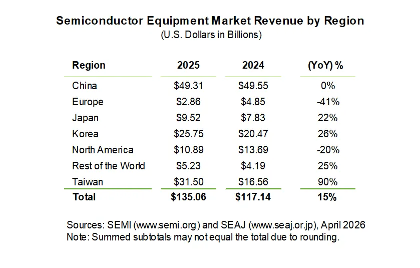
MILPITAS, Calif. – April 7, 2026 – Worldwide sales of semiconductor manufacturing equipment increased 15% to $135.1 billion in 2025 from $117.1 billion in 2024, driven by continued investment in advanced logic, memory, and AI-related capacity expansion, SEMI, the industry association representing the global electronics design and manufacturing supply chain, reported today. The data is available in the Worldwide Semiconductor Equipment Market Statistics (WWSEMS) report. 

SEMIIn 2025, the global front-end semiconductor equipment market posted solid growth, with wafer processing equipment sales increasing 12% and other front-end segments rising 13%. The expansion was driven primarily by continued investment in leading-edge logic and memory capacity, supported by AI-related demand and ongoing node and technology migrations.
The back-end equipment segment also recorded strong growth in 2025. Test equipment billings surged 55% year-over-year as AI devices and high-bandwidth memory (HBM) increased performance requirements and test intensity, while assembly and packaging equipment sales rose 21% as adoption of advanced packaging technologies continued to expand.

"Record semiconductor equipment billings of $135 billion in 2025 underscore the scale and urgency of the industry's buildout as AI accelerates demand for leading-edge logic, advanced memory and high-bandwidth architectures," said Ajit Manocha, SEMI President and CEO. "From wafer fab investments to the rapid rise of advanced packaging and test, the global ecosystem is expanding capacity and capability to support the next wave of innovation."

Regionally, semiconductor equipment spending remained concentrated in Asia in 2025, with China, Taiwan, and Korea together accounting for 79% of the global market, compared with 74% in 2024.

In 2025, spending in China remained near record levels at $49.3 billion, down just 0.5% from the prior year, as domestic chipmakers continued to invest in mature nodes and select advanced capacity. Equipment spending in Taiwan rose 90% year-over-year to a record $31.5 billion, reflecting AI- and HPC-driven capacity expansion. Korea increased 26% to $25.8 billion as investment in HBM and DRAM remained strong. 

In 2025, spending in China remained near record levels at $49.3 billion, down just 0.5% from the prior year, as domestic chipmakers continued to invest in mature nodes and select advanced capacity. Equipment spending in Taiwan rose 90% year-over-year to a record $31.5 billion, reflecting AI- and HPC-driven capacity expansion. Korea increased 26% to $25.8 billion as investment in HBM and DRAM remained strong. 

Japan recorded 22% growth to $9.5 billion, supported by continued investment in domestic advanced-node manufacturing. Europe declined 41% to $2.9 billion, marking a second consecutive year of contraction amid ongoing weakness in automotive and industrial demand. North America fell 20% to $10.9 billion as spending moderated following earlier capacity expansion. The rest of the world increased 25% to $5.2 billion, reflecting expanding activity in emerging semiconductor production markets.

Compiled from data submitted by members of SEMI and the Semiconductor Equipment Association of Japan (SEAJ), the WWSEMS report is a summary of the monthly billings figures for the global semiconductor equipment industry.

About SEMI Market Data

The Equipment Market Data Subscription (EMDS) from SEMI provides comprehensive market data for the global semiconductor equipment market. A subscription includes three reports: 

  • Monthly SEMI North American Billings Report, an early perspective of equipment market trends
  • Monthly Worldwide Semiconductor Equipment Market Statistics (WWSEMS), a detailed report of semiconductor equipment billings for seven regions and more than 22 market segments
  • Bi-annual Total Semiconductor Equipment Forecast – OEM Perspective, an outlook for the semiconductor equipment market

Download a sample EMDS report.

For more information or to subscribe, please contact SEMI Market Intelligence at [email protected]. Details on SEMI market data are available at SEMI Market Data.   

Follow SEMI Market Intelligence

Follow SEMI 

About SEMI

SEMI® is the global industry association connecting over 3,000 member companies and 1.5 million professionals worldwide across the semiconductor and electronics design and manufacturing supply chain. We accelerate member collaboration on solutions to top industry challenges through Advocacy, Workforce Development, Sustainability, Supply Chain Management and other programs. Our SEMICON® expositions and events, technology communities, standards and market intelligence help advance our members' business growth and innovations in design, devices, equipment, materials, services and software, enabling smarter, faster, more secure electronics. Visit semi.huihuidehui.workers.dev, contact a regional office, and connect with SEMI on LinkedIn and X to learn more.