downloadGroupGroupnoun_press release_995423_000000 copyGroupnoun_Feed_96767_000000Group 19noun_pictures_1817522_000000Member company iconResource item iconStore item iconGroup 19Group 19noun_Photo_2085192_000000 Copynoun_presentation_2096081_000000Group 19Group Copy 7noun_webinar_692730_000000Path
Skip to main content
Default Banner Image

United States

Belgium China France Germany India Ireland Italy Japan Malaysia Singapore South Korea Taiwan United States Vietnam Water Mgmt banner 350x317 Business Executive Technical

Thank you to our sponsors:  


         Sundt Construction Company & General Contractor | Sundt                                   SCREEN logo


Highlighted content

United States

9:00 am - 9:10 am

Welcome and Overview of the Water Management Working Group

9:10 am - 9:25 am
Pascal Osten
Leader, Water Solution Providers Cohort
Pascal Osten
DAS Environmental Expert GmbH

Procedures Guide

9:25 am - 9:35 am
Catherine Marsan-Loyer
Co-Lead, Fab, OSATs Cohort
Catherine Marsan-Loyer
C2MI

Water Savings Guide and Baseline-setting

9:35 am - 9:45 am
Jared Burdik
Co-Lead, Fab, OSAT Cohort
Jared Burdick
Sundt Corp.

Solutions Maturity Scale

9:45 am - 9:55 am

Q&A & WrapUp

EHS SMG Sustainability EMG FOA Standards

Join the SEMI Water Management team and document authors for a webinar discussing their research and findings for the Water Management Strategy Reports.  The reports are guides for water managers for understanding their water balance, baseline, potential savings and a general maturity scale for several solutions to be considered to move up the maturity scale to Zero Liquid Discharge (ZLD). The webinar will provide an overview on how the documents should be used to work with water solutions providers and provide strategies for both new and legacy facilities with end-of-pipe solutions as well as treatments for individual process stage water discharge. 

The webinar will include a discussion of next steps for the continued development of the reports, including how they interact with SEMI Standards and the industry roadmaps.

Reports can be downloaded HERE.

9:00 am - 10:00 am Off Add to Calendar 2026-05-21 09:00:00 2026-05-21 10:00:00 Water Management Strategies Webinar Join the SEMI Water Management team and document authors for a webinar discussing their research and findings for the Water Management Strategy Reports.  The reports are guides for water managers for understanding their water balance, baseline, potential savings and a general maturity scale for several solutions to be considered to move up the maturity scale to Zero Liquid Discharge (ZLD). The webinar will provide an overview on how the documents should be used to work with water solutions providers and provide strategies for both new and legacy facilities with end-of-pipe solutions as well as treatments for individual process stage water discharge. The webinar will include a discussion of next steps for the continued development of the reports, including how they interact with SEMI Standards and the industry roadmaps.Reports can be downloaded HERE. United States SEMI.org [email protected] America/Los_Angeles public America/Los_Angeles Watch the recorded webinar
Event format
Promote in calendar
On
Belgium France Germany Ireland Italy United States Security Training Featured Speakers

Course Description

This course introduces key cybersecurity principles, practices, and strategies tailored for semiconductor manufacturing environments. Participants will explore foundational concepts in cybersecurity, risk management, and best practices to secure semiconductor manufacturing systems and data.

Who Should Attend

This course is designed for:

  • Engineers and technicians in semiconductor manufacturing
  • IT professionals managing manufacturing systems
  • System administrators are responsible for securing semiconductor equipment and networks
  • Individuals tasked with implementing cybersecurity strategies in industrial settings

Prerequisites

  • Basic understanding of semiconductor manufacturing processes
  • Familiarity with IT infrastructure (networks, computers, and systems)

Learning Objectives

By the end of the course, participants will: 

  • Understand the basic principles of cybersecurity and their importance in a manufacturing environment.
  • Be able to assess and manage cybersecurity risks within the semiconductor manufacturing systems.
  • Learn practical strategies for implementing cybersecurity measures to protect critical infrastructure, devices, and data.
  • Gain insights into responding to and recovering from cybersecurity incidents.
  • Be prepared to develop and promote a strong security culture within their organization. 


Important Information

Note that only the person who registered will receive a certificate of completion. This virtual training will not be recorded. Attendees must be present to access course knowledge. 

Can't find the training link day of? After you register, you will receive the link to the live training via the email address you provided. In addition, you will receive email reminders about 24 hours in an advance and an hour before with the same link. Please keep these emails on hand to access the trainings on time. If you do not see any confirmation emails, please check your junk/spam folders before contacting SEMI U for support.

United States

Steven Hsu
TXOne Networks
SEMI U Standards

Unlock the secrets to safeguarding semiconductor manufacturing systems with this comprehensive cybersecurity course. Learn essential principles, risk management strategies, and best practices to protect critical infrastructure and data from cyber threats. Equip yourself with the knowledge to implement robust security measures and respond effectively to incidents in industrial environments.

Pricing
  • Members: $99
  • Non-Members: $129

* For group orders with 10+ attendees, and for Students/Veterans discounted pricing, please contact [email protected]. 

8:00 am - 12:00 pm Off Add to Calendar 2026-07-13 08:00:00 2026-07-13 12:00:00 Implementing Basic Cybersecurity Principles in Semiconductor Manufacturing (Virtual Training (Americas & EU) Unlock the secrets to safeguarding semiconductor manufacturing systems with this comprehensive cybersecurity course. Learn essential principles, risk management strategies, and best practices to protect critical infrastructure and data from cyber threats. Equip yourself with the knowledge to implement robust security measures and respond effectively to incidents in industrial environments.PricingMembers: $99Non-Members: $129* For group orders with 10+ attendees, and for Students/Veterans discounted pricing, please contact [email protected].  United States SEMI.org [email protected] America/Los_Angeles public America/Los_Angeles Register Now
Event format
Promote in calendar
Off

Rogue Valley Microdevices (RVM), a U.S.-based pure-play MEMS foundry, today announced the launch of its foundry-flexible MEMS Design Services, expanding its ability to support customers from early concept through production-ready device design.

This new capability allows customers to work with RVM as a design partner independent of fabrication location. Customers can develop manufacturable MEMS devices with RVM and then choose to fabricate at the foundry that best aligns with their technical requirements, capacity needs, and supply chain strategy.

RVM offers three flexible engagement models:
• Design – MEMS device design, modeling, and layout development
• Design & Technology Transfer – Design with structured transfer to a customer-selected foundry
• Design & Fabricate – Integrated design-to-manufacturing within RVM’s MEMS foundry

This approach gives customers greater control over development risk, cost, and supply chain resilience while ensuring designs are grounded in real fabrication processes from the start.

To lead this initiative, Rogue Valley Microdevices has appointed Scott Rauscher, PhD, a MEMS engineering leader with nearly two decades of experience spanning U.S. government research, defense programs, and commercial technology development.

MEMS Design Services at Rogue Valley Microdevices

The addition of design services reflects growing demand for deeper collaboration during device development and increased flexibility in selecting manufacturing partners.

“Many of our customers are pushing the boundaries of MEMS performance and integration, and that requires close collaboration between design and manufacturing,” said Jessica Gomez, CEO of Rogue Valley Microdevices. “By adding design services alongside our fabrication capabilities, we help customers accelerate development, optimize device performance, and move more efficiently from concept to commercialization. Scott Rauscher’s experience across design, modeling, and microfabrication makes him the ideal leader to build this capability.”

RVM’s Design Services support customers across key areas of MEMS development, including:
• MEMS device design and layout development
• Implementation of design rule checks and layout standards
• Design-of-experiment (DOE) array creation
• Integration of process monitors for lithography, etch, and thin film validation
• Process flow development and refinement for manufacturability

RVM’s engineering team works closely with customers to align device design with proven fabrication methods, reducing iteration cycles and improving first-pass success.
In parallel, Rogue Valley Microdevices is developing more automated design workflows using industry tools such as L-Edit and K-Layout, while advancing toward a formal Process Design Kit (PDK) to further streamline collaboration and accelerate development timelines.

Scott Rauscher Joins Rogue Valley Microdevices Team

Scott Rauscher brings extensive experience in MEMS design and technology development across both government and industry. Most recently at L3Harris Technologies, he led process architecture and technology strategy while managing a microfabrication and design engineering team. In that role, he developed critical device technology and helped grow it into a portfolio exceeding $80 million.

His career also includes leadership roles at the Naval Surface Warfare Center and the U.S. Army Research Laboratory, where he served as a MEMS device inventor and microfabrication lead. Rauscher holds more than ten patents issued and pending and has been active in industry and research organizations, including the Florida Semiconductor Institute, the MMEC consortium’s Quantum Working Group, and national semiconductor infrastructure initiatives.

“Rogue Valley Microdevices is uniquely positioned to help customers bridge the gap between innovative device concepts and manufacturable products,” said Dr. Scott Rauscher, Chief Innovation Officer, Rogue Valley Microdevices. “With the new Palm Bay facility coming online and the addition of integrated design services, we have an opportunity to build a collaborative environment where device engineers can work closely with the fab to accelerate development and scale promising technologies into production.”

The launch of Design Services marks another step forward for Rogue Valley Microdevices as it prepares to open its Palm Bay facility and expand its U.S.-based manufacturing capabilities. Together with the company’s established operations in Medford, Oregon, the new fab will strengthen domestic MEMS production capacity while providing customers with greater supply chain resilience and advanced wafer services.

To learn more about RVM’s Design Services, please contact: [email protected]

About Rogue Valley Microdevices

Rogue Valley Microdevices (RVM) is a U.S.-based pure-play MEMS foundry providing integrated design services, MEMS manufacturing, and wafer services, enabling customers to move efficiently from concept to scalable manufacturing. RVM supports the full MEMS development lifecycle, from device design and process development to volume manufacturing. By aligning design with proven fabrication processes from the outset, RVM helps reduce development risk and accelerate time to market.
With operations in Medford, Oregon, and a new 300 mm MEMS-capable facility in Palm Bay, Florida, RVM supports applications across MEMS, sensors, photonics, and specialty post-CMOS technologies. The company serves customers in industries including healthcare and biotech, industrial sensing, aerospace and defense, communications, and advanced electronics. By combining collaborative design expertise, flexible process development, and domestic manufacturing capability, RVM delivers a transparent, customer-focused approach that strengthens supply chain resilience and provides a clear path from innovation to volume manufacturing.
For more information, visit www.roguevalleymicro.com

Media Contact:
Maria Doyle
Doyle Strategic Communications (for Rogue Valley Microdevices)
781-964-3536
[email protected]

Registration

2025_MedTech_photo1

Regular Pricing
$249 Members
$349 Non-Members

Cancellation Policy

Cancellations received on or before July 27, 2026, are fully refunded with a $50 processing fee. Refunds will not be issued for cancellations (including no-shows) made after July 27, 2026, and only substitutions are accepted with a written note from the registered attendee. Please email your cancellations or substitutions on company letterhead to [email protected].

2025_MedTech_photo1
United States Smart Medtech Summit 2026 Technical
GlobalFoundries
Keynotes

Breaking Silos, Accelerating Innovation: Semiconductor & MedTech Converge Together

In a rare cross-industry gathering, MedTech pioneers and semiconductor innovators are coming together under one roof. The Semiconductor–MedTech Ecosystem Summit is designed to break down industry silos, connecting silicon innovators directly with medical device makers to accelerate the development of next-generation medical technology.

If you are building the future of medical devices, diagnostics, or connected care, this is where you secure your competitive advantage.

The Convergence: Three Focus Areas Driving the Next Frontier

By bringing these two massive industries together, we are accelerating the timeline for revolutionary healthcare. We will be diving deep into:

  • Wearables & Continuous Care: Changing the game for personalized healthcare by enabling clinical-grade, untethered monitoring that moves with the patient.
  • Advanced Medical Imaging: Pushing the boundaries of early detection through advanced imaging technologies that make the unseen visible.
  • Edge AI & Predictive Health: The invisible engine underpinning rapid advancements in both MedTech and silicon. We’ll explore how processing at the edge allows for the pinpointing of diagnoses and treatments long before traditional symptoms appear.

SEMI Headquarters
673 S. Milpitas Boulevard
Milpitas, CA 95035
United States

Marc Schaepkens
Marc Schaepkens
Chief Technology Officer, Advanced Imaging Solutions
GE Healthcare
Laura Matz, Merck KGaA
Laura Matz
Chief Science & Technology Officer
Merck KGaA
Ahmad Bahai, Texas Instruments
Ahmad Bahai
Senior Vice President & Chief Technology Officer
Texas Instruments

Breakfast & Registration

8:00 am - 9:00 am

Breakfast & Registration

Strategic Outlook

9:00 am - 9:15 am
Ajit_circle_photo-v2.png
Ajit Manocha
CEO
SEMI

Welcome Address

SEMI Perspective
Biography

9:15 am - 9:30 am
Mike Hogan Tile
Michael Hogan
Chief Strategy Officer
GlobalFoundries

Welcome from GlobalFoundries

9:30 am - 9:50 am
Marc Schaepkens
Marc Schaepkens
Chief Technology Officer, Advanced Imaging Solutions
GE Healthcare

Keynote: No Chips, No Cure: Why Semiconductors Are the Invisible Infrastructure of Modern Healthcare

9:50 am - 10:05 am
Derrick
Derrick Kiker
McKinsey & Company

The Life Sciences Growth Engine Runs on Silicon

Networking

10:05 am - 10:30 am

Break

Integration

10:30 am - 10:50 am
Laura Matz, Merck KGaA
Laura Matz
Chief Science & Technology Officer
Merck KGaA

Keynote: Exploring Enabling Approaches for Precision Medicine throughout the Drug Development Process

10:50 am - 11:05 am
Joshua De Souz Headshot
Joshua De Souza
Senior Principal Scientist
Medtronic

From Integration to Intervention: The Whole is Greater than the Sum of its Parts

11:05 am - 11:20 am
Paru Deshpande
Paru Deshpande
VP Health Technologies
IMEC

Bioconvergence: How Semiconductor Innovation is Shaping the Future of Healthcare

11:20 am - 12:00 pm

Panel Discussion: The Role of Semiconductor in 5-10 Years in MedTech

Session Chair - Anirban Bandyopadhyay
Fritz Werder | Silicon Labs
Mohsen Askarinya | Medtronic
Girish Naganathan | Former Dexcom
Paru Deshpande | imec
Lea Drye | FDA

Networking

12:00 pm - 1:00 pm

Lunch

Innovation

1:00 pm - 1:20 pm
Ahmad Bahai, Texas Instruments
Ahmad Bahai
Senior Vice President & Chief Technology Officer
Texas Instruments

Keynote: "Health Sciences, Semiconductor & AI" A Transformational Confluence

1:20 pm - 1:35 pm
Pieris Berreitter
Pieris Berreitter
Director of Engineering
HP

Inference on the Edge: The Next Generation of Wearable Silicon for Healthtech

1:35 pm - 1:50 pm
Mauro Ferrari headshot 2026
Mauro Ferrari
Chief Executive Officer
BrYet

Microfabbed Silicon as a (Transformational) Pharmaceutical Material

1:50 pm - 2:30 pm

Panel Discussion: Disruptive Innovation in MedTech for Therapeutic and Diagnosis

Session Chair - Melissa Grupen-Shemansky
Vibhu Sharma | Philips
Bharath Rajagopalan | STMicroelectronics
Laura Matz | Merck KGaA
Gregg Bartlett | GlobalFoundries

Networking

2:30 pm - 2:45 pm

Break

Innovation

2:45 pm - 3:00 pm
Bharath Rajagopalan, STMicroelectronics
Bharath Rajagopalan
Director of Strategic Marketing
STMicroelectronics

Semiconductor Innovations Enabling the Future of Healthcare

3:00 pm - 3:15 pm
Vibhu Sharma Philips
Vibhu Sharma
Biosubstrates Program Lead
Philips

When Biology Becomes the Sensor: Semiconductor-Enabled Platform for Cellular Intelligence

3:15 pm - 3:30 pm
Yusuf
Yusuf Haque
Cofounder & Chief Technology Officer
Exo Imaging

Democratization of Ultrasonic Medical Imaging & Challenges

3:30 pm - 3:45 pm
Girish_Naganathan
Girish Naganathan
Former CTO
EVP Dexcom

Beyond the Form Factor

3:45 pm - 4:00 pm

Wrap Up

SEMI

Networking

4:00 pm - 6:00 pm

Reception

Smart MedTech

Experience a one-of-a-kind convergence of silicon and clinical care. Connect directly with semiconductor foundries and MedTech OEMs on Aug 27 to accelerate next-gen medical devices.

8:00 am - 6:00 pm Off Add to Calendar 2026-08-27 08:00:00 2026-08-27 18:00:00 Semiconductor-MedTech Ecosystem Summit Experience a one-of-a-kind convergence of silicon and clinical care. Connect directly with semiconductor foundries and MedTech OEMs on Aug 27 to accelerate next-gen medical devices. SEMI Headquarters 673 S. Milpitas Boulevard Milpitas, CA 95035 United States SEMI.org [email protected] America/Los_Angeles public America/Los_Angeles
Recommended Hotels

Embassy Suites by Hilton Milpitas Silicon Valley

901 East Calaveras Boulevard

Milpitas, CA 95035

(408) 942-0400


Courtyard by Marriott Milpitas Silicon Valley

1480 Falcon Dr.

Milpitas, CA 95035

(408) 719-1966

Register Here!
Event format
Tab Order
Overview
Agenda
Sponsors
New Tab 1
Promote in calendar
Off

High-performance connectivity software delivers structured, high-volume equipment data required by tier-one fabs and advanced packaging facilities ahead of the expected mid-2026 SEMI standards update

POITIERS, March 25, 2026 – Agileo Automation, a leading provider of control and connectivity solutions for global semiconductor manufacturing, today unveils Agil'EDA, a new software solution implementing Equipment Data Acquisition (EDA), a set of SEMI standards also known as Interface A, to enable semiconductor equipment manufacturers to meet the evolving high-performance connectivity requirements of tier-one fabs and advanced packaging facilities.

As semiconductor manufacturing moves towards higher levels of automation and data-driven optimization, fab owners increasingly require EDA alongside traditional SECS/GEM connectivity from semiconductor OEMs for their production tools. Agil'EDA addresses this by separating the control flow from the data flow, ensuring that structured, high-frequency data collection does not interfere with critical equipment operations.
Designed for long-term deployment, Agil'EDA fully supports the widely used EDA Freeze 2 (SOAP/XML) and is architected for the transition to Freeze 3 (gRPC/protocol buffers). This next-generation standard offers significantly higher data throughput and reduced latency. Agileo has already successfully tested and validated its EDA Freeze 3 implementation at SEMI’s North America Standards Fall Meetings in November 2024 in Milpitas, California. SEMI’s EDA Freeze 3 standards suite is expected to be released mid-2026.

Complementing the SECS/GEM standards used to control equipment behavior, Agil’EDA incorporates robust cybersecurity features such as authentication and encrypted communications. The product is available as a stand-alone solution for any existing equipment software using a platform-independent gRPC application programming interface (API) to communicate with it or as a pre-integrated component within Agileo’s A²ECF-SEMI framework. When used with Agil'GEM and Agil'GEM300, it provides a comprehensive connectivity solution that significantly reduces time to market for OEMs.

"With the growing demand for data to improve yield in tier-one fabs, as well as in Advanced Packaging and 3D integration, EDA is no longer optional. It is becoming a mandatory requirement for equipment entering the world's most advanced fabs," explains Marc Engel, chief executive officer of Agileo Automation. "The key value we deliver for OEMs is a fast and easy adoption path for a seamless EDA architecture that delivers compliant production machines to global fab customers. By providing a future-proof architecture ready for Freeze 3, which will significantly increase performance, we address OEMs’ current needs while preparing them for the evolving requirements of semiconductor manufacturing, including AI-driven process control."

- ends -

About Agileo Automation
Agileo Automation is a trusted partner for equipment manufacturers, helping them build smarter, automated, and more connected machines that integrate seamlessly into advanced semiconductor fabs. Founded in 2010 in Poitiers, France, Agileo helps OEMs with control, communication, data acquisition, and testing across their tools through proven software and expert support. Its flagship A²ECF-SEMI framework provides a solid foundation for developing equipment controllers fully aligned with SEMI SECS/GEM, GEM300, and EDA standards. As an active member of SEMI and the OPC Foundation, Agileo Automation contributes directly to shaping the standards that drive manufacturing. For more information, please visit our website or follow us on LinkedIn.

Belgium France Germany Ireland Italy United States Seimconductor Device Assembly Training

Course Description 

This three-day virtual workshop (4 hours a day) provides a complete overview of the semiconductor manufacturing process. The class focuses on key process steps needed to form a functioning device. Some important science and engineering ideas needed to understand device manufacturing will be discussed. The workshop is designed for non-technical personnel needing an understanding of the fab process steps.  Some technical background from attendees will improve the workshop learning. 

The first day will overview the fab process steps with a brief summary of how a transistor functions. We will discuss how multiple transistors are connected to form a logic or memory device. We will also cover how a transistor works with respect to the physical layout of Bipolar and MOSFET transistors. 

The second day will cover key fab process steps. Ion implantation, photolithography including DUV and EUV processes, plasma processes including deposition and etch, rapid thermal processing, and wet etch processing. Specific emphasis will be given to the different wet etch processes. 

The third day of the workshop will focus on the new transistor designs, including FinFET and CFET designs. We will also cover reasons for changing the transistor design and newer materials, including tantalum, hafnium, silicon germanium, and low-k dielectrics.  We will also review roadmaps of leading companies, including TSMC, Intel, and Samsung. 

After completing the workshop, the student will be able to describe all the fabrication and assembly process steps and have an understanding of how the process steps work together to form the completed integrated circuit, in addition to an understanding of future structures.


Who Should Attend

This course is intended for both manufacturing and R&D know-how in IC packaging professionals, including but not limited to:

  • Process Technicians
  • Material Engineers
  • Process Engineers
  • Equipment Manufactures
  • Technical Marketing Engineers

Topics Included

  • Silicon wafer manufacturing
  • Basic operating principles of transistors and semiconductor devices
  • Planar, FinFET, and GAA transistor formation and design differences
  • Fab processes needed to form a semiconductor, including the following:
    • Lithography, with a focus on DUV and EUV methods
    • Etching, including wet and plasma processes
    • Deposition, thermal, plasma, electroplating deposition
    • CMP and modern CMP processes
       

Important Information

Note that only the person who registered will receive a certificate of completion. This virtual training will not be recorded. Attendees must be present to access the course knowledge. 

Can't find the training link on the day of? After you register, you will receive the link to the live training via the email address you provided. In addition, you will receive email reminders about 24 hours in advance and an hour before with the same link. Please keep these emails on hand to access the training on time. If you do not see any confirmation emails, please check your junk/spam folders before contacting SEMI U for support.


Dr. Tom Dory
ITM Consulting, Inc

United States

- SEMI U

Unlock the essentials of the semiconductor manufacturing process.  We will cover science and engineering concepts needed to understand device manufacturing. 

Pricing         

              Early Bird Pricing: $100 off

  • Members:  $699   $599
  • Non-Members:  $749   $649

* For group orders with 10+ attendees, and for Students/Veterans discounted pricing, please contact [email protected].

8:00 am - 12:00 pm Off Add to Calendar Disabled America/Los_Angeles Register Now
Event format
Promote in calendar
Off

SEMI Members:  $75

Use your corporate email address during log in to be recognized as a SEMI Member.

Non-Members:  $149

Students:  Free

Contact Basak Ulutas Ozturkler ([email protected]) with a picture of your student ID to receive your discount code.

Belgium Germany Singapore Taiwan United States FEMC 29 recording Business Executive Technical
Highlighted content

Digital Twin is a virtual representation of the structure, context, and behavior of physical systems or a process, with a live link to a physical system serving as a key enabler for predictive and data-driven optimization. In Printed and Flexible Hybrid Electronics (FHE), manufacturing involves multiple interdependent variables—different printing technologies, inks, substrates, and process conditions—each introducing its own complexity. In practice, additional challenges such as equipment drift, batch-to-batch variations, and environmental fluctuations further impact process consistency and yield. Changing a process or transferring it between tools is often difficult, as each setup is highly customized and sensitive to local conditions. To address these challenges, Digital Twin frameworks connect data from design, fabrication, and metrology into continuously learning digital models. They enable early detection of process drifts, virtual experimentation for process development, and data-driven optimization that reduces time, cost, and waste.

This course introduces Digital Twin frameworks for FHE, focusing on Deep Neural Network (DNN)-based predictive models. Participants will learn how to integrate design, fabrication, and metrology data into continuously learning virtual twins that detect process drifts, enable virtual experimentation, and optimize manufacturing. The program covers the full workflow—from image processing and virtual metrology to AI model training, validation, and hyperparameter tuning—using real datasets. A hands-on “Build Your Own Digital Twin” module in Google Colab will provide practical experience in training and refining models for printed electronics applications, equipping attendees with both theoretical insight and applied skills for process optimization and performance prediction.

ABOUT THE SPEAKER

Benyamin Davaji, PhD
Benyamin Davaji is an Assistant Professor in the Department of Electrical and Computer Engineering at Northeastern University, Boston, Massachusetts, where his research centers on integrated microsystems for sensing and computation using mechanical waves. His work spans acoustic and ultrasound transducers, biointerfaces, and microcalorimetry, with a strong emphasis on data-guided nanofabrication, advanced semiconductor device manufacturing, and interdisciplinary approaches to microsystem design and manufacturing. He earned his Ph.D. in Electrical and Computer Engineering from Marquette University in 2016 and completed a postdoctoral appointment at Cornell University.

United States

Davaji Profile picture
Ben Davaji, PhD
Assistant Professor
Northeastern University
Gity Samadi
Moderator
Gity Samadi, PhD
Sr. Director, R&D Programs
SEMI
NBMC Smart MedTech FlexTech

Join us for a Master Class with Benyamin Davaji, PhD, as he introduces Digital Twin frameworks for Printed and Flexible Hybrid Electronics, demonstrating how AI- and DNN-based models integrate design, fabrication, and metrology data along with printing technologies to detect process drift, enable virtual experimentation, and optimize manufacturing performance. Participants gain hands-on experience building continuously learning digital twins to reduce variability, cost, and time to optimization. 

10:00 am - 12:00 pm Off Add to Calendar 2026-06-10 10:00:00 2026-06-10 12:00:00 FEMC#29 Digital Twins for Printed Electronics: How Can AI Learn FHE Printing? Join us for a Master Class with Benyamin Davaji, PhD, as he introduces Digital Twin frameworks for Printed and Flexible Hybrid Electronics, demonstrating how AI- and DNN-based models integrate design, fabrication, and metrology data along with printing technologies to detect process drift, enable virtual experimentation, and optimize manufacturing performance. Participants gain hands-on experience building continuously learning digital twins to reduce variability, cost, and time to optimization.  United States SEMI.org [email protected] America/Los_Angeles public America/Los_Angeles Watch on-demand
Event format
Promote in calendar
Off
Belgium France Germany Ireland Italy United States Fundamentals of ALD, ALE and Precursors Chemistries Training

Course Description 

This course provides a practical introduction to atomic layer deposition, an essential technique in semiconductor manufacturing. You'll learn about ALD foundational concepts, including growth, advantages, measurements, and more, chemical precursors for use in ALD, selected ALD processes, area-selective deposition, and atomic layer etching. Overall, the applications and chemistry used in semiconductor processing, as they relate to ALD and ALE, are heavily discussed.

Who Should Attend

This course is intended for both manufacturing and R&D know-how in IC packaging professionals, including but not limited to:

  • Engeineers
  • Managers
  • Process Engineers
  • R&D Engineers
  • Sales and Application Engineers who supply packaging materials and tools

Learning Objectives

  • Understanding foundational concepts of ALD.
  • Describe chemical precursors for ALD applications.
  • Identify selected ALD processes and their associated films and materials. 
  • Explain area-selective deposition (ASD), and its uses.
  • Describe Atomic Layer Etching (ALE) concepts and understand it's relationship to ALD.


Important Information

Note that only the person who registered will receive a certificate of completion. This virtual training will not be recorded. Attendees must be present to access the course knowledge. 

Can't find the training link on the day of? After you register, you will receive the link to the live training via the email address you provided. In addition, you will receive email reminders about 24 hours in advance and an hour before with the same link. Please keep these emails on hand to access the training on time. If you do not see any confirmation emails, please check your junk/spam folders before contacting SEMI U for support.

United States

Dr. Chuck Winter
Dr. Chuck Winter
Instructor
- SEMI U

Discover how atomic-scale precision is revolutionizing semiconductor manufacturing with Atomic Layer Deposition (ALD) and Etching (ALE). Course topics include ALD foundational concepts, Chemical Precursors and Processes, and Advanced ALD Techniques. 

Pricing

          Early Bird Pricing $100 off

  • Members: $845   $745
  • Non-Members: $945  $845

* Group pricing for 20+ attendees: $9900
Any questions, please contact [email protected]

7:30 am - 11:30 am Off Add to Calendar Disabled America/Los_Angeles Register Now
Event format
Promote in calendar
Off

Brings Advocacy for the adoption of RISC-V processors and processor verification tool standards

Leverages broad experience in EDA business strategy, marketing and sales

SAN JOSE, Calif., March 05, 2026 (GLOBE NEWSWIRE) -- Breker Verification Systems today named Larry Lapides, former Synopsys Executive Director of RISC-V Tools Business Development, to its Advisory Board.

In making today’s announcement, David Kelf, Breker’s CEO, noted that Lapides has been a tireless advocate for the adoption of RISC-V processors and the urgent need for RISC-V processor verification tool standards. “Larry’s RISC-V knowledge and his ties to the RISC-V community are welcome additions to Breker and our advisory board.”

“Breker sits at the forefront in the development of commercial processor verification solutions and is a valued member of the RISC-V community,” remarks Lapides. “It will be a pleasure to work with Breker to move this important effort forward.”

Larry Lapides Biography
Lapides joined Synopsys through the acquisition of Imperas Software, where he was Vice President of Worldwide Sales and Marketing. He previously ran worldwide sales at EDA companies including Verisity Design and has more than 30 years in software tools and EDA, plus time spent in infrared systems engineering.

Lapides holds a Bachelor of Arts degree in Physics from UC Berkeley, a Master of Science degree in Applied Physics from Cornell University and an MBA from Clark University in Worcester, Mass.

About Breker Verification Systems
Breker Verification Systems solves complex semiconductor challenges across the functional verification process from streamlining UVM-based testbench composition to execution for IP block verification, significantly enhancing SoC integration and firmware verification with automated solutions that provide test content portability and reuse. Breker’s solutions include a SystemVIP library of scenarios for RISC-V and Arm, core and SoC testing, coherency, security and other critical areas. Breker solutions easily layer into existing environments and operate across simulation, emulation, prototyping, and post-silicon execution platforms. Its Trek family is production-proven at leading semiconductor companies worldwide and enables design managers and verification engineers to realize measurable productivity gains, speed coverage closure and easy verification knowledge reuse. As a leader in the development of the Accellera Portable Stimulus Standard (PSS), privately held Breker has a reputation for dramatically reducing verification schedules in advanced development environments. Case studies that feature Analog Devices, Broadcom, IBM and other companies leveraging Breker’s solutions are available on the Breker website.

Engage with Breker at:
Website: www.brekersystems.com
Twitter: @BrekerSystems
LinkedIn: https://www.linkedin.com/company/breker-verification-systems/

TrekSoC, TrekSoC-Si, TrekBox and SoC Scenario Modeling are registered trademark of Breker Verification Systems. Breker Verification Systems acknowledges trademarks or registered trademarks of other organizations for their respective products.

SurplusGLOBAL has rolled out a set of upgrades to SemiMarket (www.SemiMarket.com), its online marketplace for legacy semiconductor equipment and parts, aimed at making inventory discovery more actionable and sourcing workflows more practical for engineers and procurement teams operating in the secondary supply chain.

A central update is the expansion of how SemiMarket publishes and organizes Harvest-completed parts. The platform has opened Special Event sections that group harvested inventories by their "parent" tool, enabling buyers to navigate end-of-life components in the same equipment-centric structure fabs use for maintenance planning and spares management. By surfacing harvested parts in a tool-based format within the marketplace, SurplusGLOBAL says SemiMarket is becoming a more direct channel for sustaining older tool fleets as OEM availability thins or ends.

SemiMarket is also adding functionality for high-volume sourcing and internal review. A new bulk download feature lets users request an item list by selecting a top-level category and clicking "Download list" from the front-end interface. Once approved by the operations team, the file becomes available for download. SurplusGLOBAL positions the tool as a practical bridge between marketplace browsing and the internal processes procurement groups use to compare options, circulate listings, and document sourcing decisions at scale.

The changes address a growing pain point across mature-node fabs: when a single discontinued spare can sideline a tool, downtime can extend while teams source across brokers, refurbishers, and regional networks. The legacy spares supply chain remains fragmented, and even organizations with donor-tool pools often face challenges extracting, verifying, and redeploying parts efficiently at scale. SurplusGLOBAL says the trend is increasingly reaching 300mm tools manufactured before 2010, intensifying demand for more structured, searchable legacy parts supply.

To respond, the company says it is expanding its Harvest program—disassembling used equipment and remarketing parts—supported by in-house verification and data standardization. SurplusGLOBAL said it has harvested about 60 tools to date and plans to harvest roughly 200 to 300 tools this year, backed by teams spanning Harvest operations, parts verification, AI, SemiMarket, database engineering, and sales.

The company also said it is applying AI and OCR-driven workflows to accelerate classification, imaging, standardization, and listing creation, while building tool–part relationships, parts BOM coverage, and personalized recommendations.

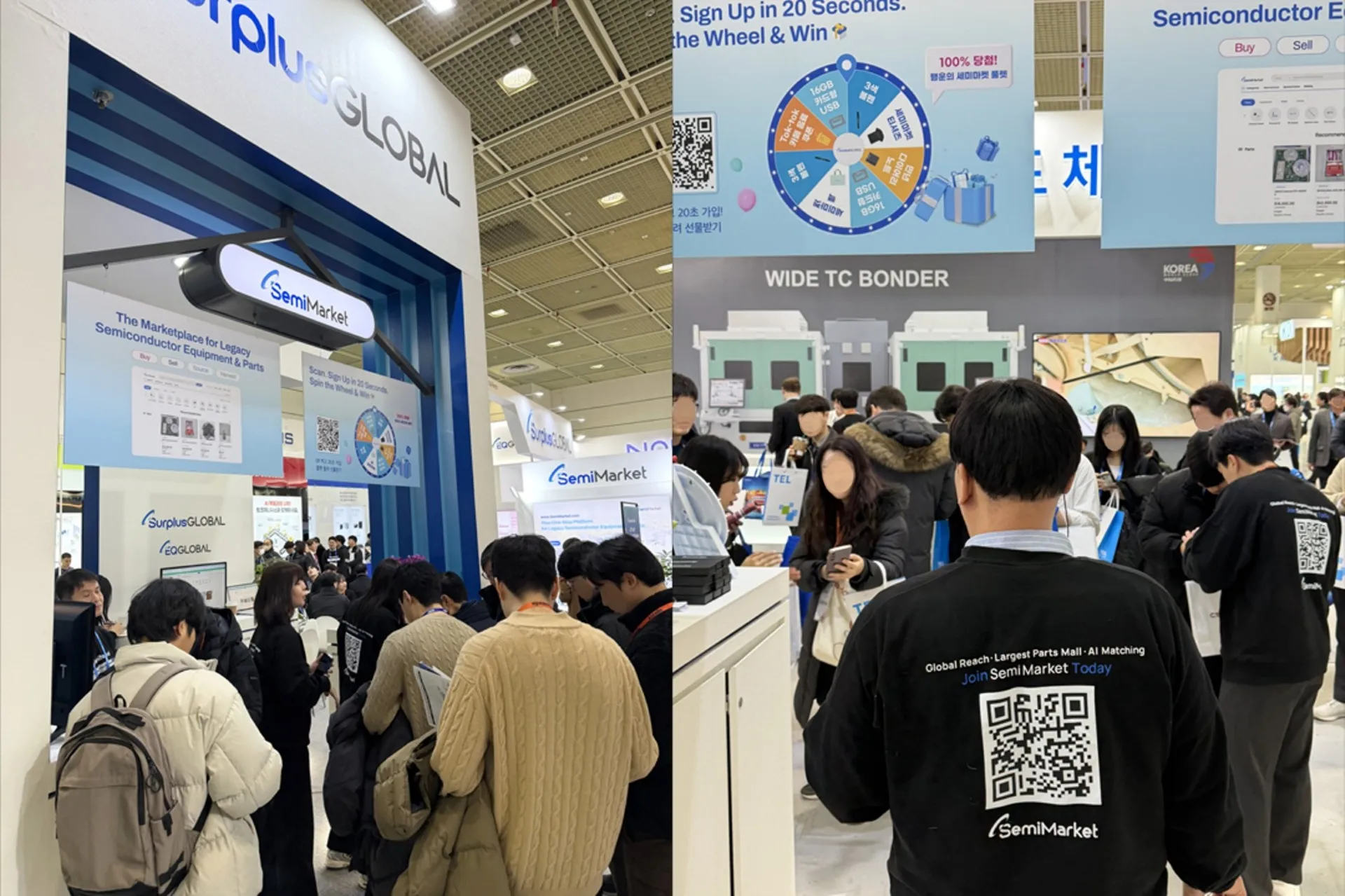
The upgrades follow a recent rise in platform engagement tied to industry events. During SEMICON KOREA 2026, held Feb. 11–13 at COEX in Seoul, SurplusGLOBAL said about 3,000 industry visitors stopped by its booth and more than 800 signed up for SemiMarket on-site. The company said many of the new members included process and maintenance engineers, as well as employees from global equipment makers—roles closely connected to day-to-day tool operation and purchasing decisions.

Bruce Kim, SurplusGLOBAL's CEO, said the updates reflect "growing demand for faster, clearer decision-making and more actionable inventory discovery in the mature-node ecosystem, where uptime pressures and supply variability often push teams beyond OEM channels." He added that the company is expanding Harvest-led supply and improving how SemiMarket organizes that inventory so buyers can move from discovery to decision more quickly.

SurplusGLOBAL also pointed to a near-term offline expansion intended to complement online sourcing. The company said a 39,670m2(12,000-pyeong) SemiMarket Offline Parts Mall is scheduled to be completed in July, enabling customers to view large-scale inventory in person and access services such as parts verification and repair, strengthening global support for legacy tool sustainment.