downloadGroupGroupnoun_press release_995423_000000 copyGroupnoun_Feed_96767_000000Group 19noun_pictures_1817522_000000Member company iconResource item iconStore item iconGroup 19Group 19noun_Photo_2085192_000000 Copynoun_presentation_2096081_000000Group 19Group Copy 7noun_webinar_692730_000000Path
Skip to main content
Default Banner Image

Technology and Trends

Artificial intelligence (AI) is scaling at a pace that is reshaping semiconductor roadmaps, data center design, and long-term infrastructure strategy. AI promises many economic and social benefits; but the growth comes with an escalating demand for power, and energy has emerged as a major challenge.SEMI, as the global semiconductor and electronics association connecting over 4,000 companies, continues to unite the entire ecosystem to “bend the curve” – to maximize AI performance while minimizing power consumption. In a series of successful, sold-out workshops that the SEMI Smart Data-AI Initiative held on this topic, a resonant theme has emerged: sustaining AI progress requires energy-efficient computing with holistic co-design and co-optimization across materials, devices, systems, data transmission, data centers, emerging architectures and software. While this dialog is an important starting point, the ultimate goal is to drive concrete action through collaborative innovation.The AI Energy ChallengeAI training compute for frontier models is growing at an estimated 4–5x per year, driving unprecedented demand for hardware capability and infrastructure capacity. That trajectory has resulted in a global “data center gold rush” and is testing energy availability limits. As model sizes scale exponentially, so too does the energy required to train and deploy them; and power consumption has become a significant limiter to performance gains. Further, this increases heat dissipation, and requires innovations like direct liquid cooling.Modern AI and high-performance computing systems now operate at levels comparable to small cities, with tens of megawatts per installation and a trajectory toward gigawatt-scale data center campuses. Grid capacity—both in the U.S. and globally—may be challenged to keep pace with projected demand. Thus, AI infrastructure is no longer just a technical challenge, but it is an energy, systems, and policy challenge.System-Technology Co-OptimizationContinuous advances in chip and inference efficiency have delivered orders-of-magnitude improvements over many decades. These gains must now be expanded by holistic co-optimization of the entire compute system from silicon technologies to data center to the grid.For example, processors can be made more efficient by customizing them for specific workloads. However, only part of total data center power is consumed by the processor itself. A significant portion is used by data movement, power conversion and cooling. The energy required to move data increases dramatically with distance. Moving bits across packages, boards, and networks can consume far more energy than the compute operations themselves. This makes locality a critical design principle. The opportunity—and necessity—therefore lies in cross-layer optimization: efficient compute, efficient communication, and intelligent power management across the entire system. Not surprisingly, advanced packaging and integration are becoming central to performance. These technologies can enable architectures that tightly couple compute, memory, and I/O—using 2.5D and 3D integration techniques—reducing energy per bit and increasing bandwidth. Photonic interconnects and low-power materials can further lower the cost of processing and moving data.The bottom line is that incremental chip-level gains alone will not be sufficient and energy optimization cannot be siloed—system-technology co-optimization is needed.Hardware-Software Co-optimizationKeeping data as localized as possible depends as much on software algorithms as it does on hardware architectures. The challenge is that the development cycles are mismatched: new software models can be developed in months, while designing and fabricating new hardware can take years. While this cycle mismatch is fundamental, closer coordination between hardware and software developers can significantly improve efficiency. For example, offloading selected functions in the algorithm, including distributed DPUs, and reducing the level of data precision can reduce energy use. Partitioning workloads logically across the hardware/software stack between cloud services and compute-on-edge can also reduce energy appreciably. Further, risk mitigation techniques—for example, building in strategic redundancy—can make future designs more resilient to shifts in software algorithms and models.Diverse Computing ModalitiesWhile AI dominates current infrastructure investment, the future of computing will likely include multiple, diverse computational modalities such as quantum, neuromorphic, photonic and analog computing.Different computational paradigms will be applied where they are most effective. For example, quantum computing is likely to complement—not replace—classical systems; especially for specific classes of problems where it offers exponential advantages. However, progress in quantum computing is tightly coupled to advances in semiconductor infrastructure. Error correction, orchestration, and hybrid algorithms all depend on high-performance classical systems operating with low latency alongside quantum processors. While there is no single silver bullet, system-level design can ensure that multiple computing modalities work together within unified workflows spanning edge, cloud, and exascale environments.Why It Matters What to WatchEnergy will now be a key constraint for AI performance and infrastructure expansion.The evolution of gigawatt-scale AI campuses and their interaction with public energy grids will accelerate – or slow down – AI growth.Data movement, memory bandwidth, interconnect efficiency, advanced packaging and heterogeneous integration will be strategic levers. Enhanced system-technology co-optimization and integration of advanced technologies like 3D ICs and photonics will be critical.Co-optimization across hardware, software, and systems will be required.Future architectures will blend classical and emerging compute modalities like quantum, photonic and neuromorphic.In conclusion, AI has become a defining global force with much promise, but its trajectory will be shaped by technology, energy and infrastructure economics working together. This is a formidable challenge because it requires many diverse players with divergent priorities to collaborate effectively.We invite you to join the SEMI Smart Data-AI initiative to collaboratively address this challenge and help realize AI’s full potential sustainably. Our next workshop in this series will be on September 9 in Silicon Valley – please join us for this exciting event.SourcesSEMI Smart Data-AI Initiative – Future of ComputingEnergy-Efficient Computing for AI and Beyond, SEMICON West, October 2025Sustainable AI Systems, SEMI HQ, March 2026About the AuthorsDr. Pushkar P. Apte is the Strategic Technology Advisor for SEMI Global Lead for the Smart Data-AI Initiative Dr. Melissa Grupen-Shemansky is Senior VP and CTO of SEMI
Read More
The SEMI Standards team hit the ground running in 2026, starting this year with an important milestone to our Flexible Hybrid Electronics (FHE) standardization efforts. As FHE technology continues to evolve into a scalable and manufacturable class of systems, we’re excited to share the upcoming release of SEMI 7242, Guide for Reliability of Flexible Hybrid Electronics. This is the first time a comprehensive framework for reliability assurance in FHE systems has been created, closing a critical gap within the industry landscape. Published as SEMI FH5, the standard is now available online via the SEMI Store or through a SEMIViews license.We’d also like to highlight a pending revision for SEMI E142, Specification for Substrate Mapping. While SEMI E142 is currently designed to work with other SEMI data exchange Standards, SEMI Draft Document 7381 proposes a subordinate standard to define maps to and from non-E142 wafer coordinate systems. Meanwhile, the Information Control Japan Technical Committee (TC) announced its new Maintenance Robot Communication (MRC) Task Force for standardizing communications for robotic maintenance systems to improve production efficiency and workloads in fabs. This quarter also included key developments from both SEMICON Korea and SEMICON China. At SEMICON Korea, members of the Semiconductor Manufacturing Cybersecurity Consortium (SMCC) discussed a unified, standards-based approach for strengthening cybersecurity amidst evolving digital threats. A month later, SEMICON China served as the backdrop for the EHS TC Chapter Formation Group Meeting, where attendees discussed critical safety, material usage, and energy efficiency standards. The North America (NA) Winter Meetings, held virtually in February 2026, also brought several TCs together to revise standards for MEMS, advanced packaging, EH S, Facilities, Gases Liquid Chemicals, factory automation, and more. For more than 50 years, the SEMI Standards International Program has worked to advance manufacturing processes, lower costs, and support key industry growth markets. To get involved in future developments, become a member of the SEMI Standards Program. Membership is free.With so much underway in Q1, we look forward to an incredible year ahead. Q1 2026 Highlights A New Standard for Flexible Hybrid Electronics As the first consensus-driven framework for reliability assurance in FHE systems, SEMI 7242, Guide for Reliability of Flexible Hybrid Electronics, was created to ease roadblocks for transitioning and commercializing FHEs. It aims to speed design cycles, improve comparability of test results, reduce the risk of integrating FHE into operations, and instill confidence for scaling FHEs from prototypes to high-volume production. Document 7242 was drafted by the FHE Reliability and Testing Task Force, with added participation from industry, academia, and government laboratories.The elevation of Document 7242 to a formal SEMI Standard reflects the field’s progression to a stage where consistent approaches to reliability are both feasible and necessary. As FHE adoption grows across medical, industrial, consumer, and defense applications, Document 7242 will support systems that offer dependable performance and sustained durability over time. Document 7242 also joins the recently published SEMI FH6 Standard on FHE Terminology.Revisions to SEMI E142SEMI E142, Specification for Substrate Mapping, defines data items required for reporting, storing, and transmitting map data for substrates. It was developed to work alongside other SEMI Standards to exchange data through a SECS/GEM interface. Identifying failure points requires a two-dimensional XY coordinate map generated for substrates. However, because some steps in the semiconductor manufacturing process may use their own XY coordinate systems, a revision is currently needed to define an infrastructure for mapping a non-E142 wafer XY coordinate system to and from the E142 Standard XY coordinate system.The Advanced Backend Factory Integration (ABFI) Task Force will ballot this potential subordinate standard from August 19 to September 18. It will be adjudicated during SEMICON West from October 13-15, 2026 in San Francisco, California.Introducing the Maintenance Robot Communication Task Force As the industry moves toward smart manufacturing, integrating robot-based maintenance solutions is becoming increasingly important for enhancing production efficiency, reducing workload, and ensuring consistent work quality in automated environments. The Maintenance Robot Communication TF was formed to address the critical need to standardize operational communications for robotic maintenance systems. A dedicated community page is now available on the Connect@SEMI platform for members to exchange ideas. This activity joins the recently established Mobile Maintenance Robot Safety Task Force which aims to develop new safety guidelines that are deemed necessary to fill the gaps between existing industry standards including SEMI Safety Guidelines with regard to safe operation of mobile maintenance robots.Standards Activities from Europe Spring MeetingThe Compound Semiconductor Materials Europe TC Chapter held its annual virtual Spring Meeting on April 14, 2026. The meeting drew robust participation from China, Japan, Europe, North America, and other regions. The TC Chapter successfully adjudicated document 7111, Revision of SEMI M81-0418, Guide for Defects Found in Monocrystalline Silicon Carbide Substrates. The major update provides significant guidance on defects in silicon carbide substrates. This document has been forwarded to SEMI Publications for final processing. The Europe TC Chapter will reconvene November 10–13, 2026, during SEMICON Europa in Munich, Germany.Underscoring the Need for Cybersecurity Standards at SEMICON Korea SEMICON Korea featured more than 200 speakers who shared insights and presented solutions that are shaping the modern AI era. From February 11-13 in Seoul, the conference also served as a meeting point for the next generation of SEMI Standards. Most notably, leaders from the Semiconductor Manufacturing Cybersecurity Consortium (SMCC) highlighted the strategies and operational frameworks needed to modernize cybersecurity protocols. SEMICON Korea Highlights:Applied Materials’ Suk Won Kang discussed SMCC Working Group (WG) 9 – a new group for addressing cybersecurity challenges unique to South Korea’s semiconductor ecosystem. WG9 was formed to better understand Korean cybersecurity risks, align with global standards, and operationalize compliance with existing SEMI frameworks. Alan Weber from PDF Solutions presented on cybersecurity as it relates to industry standards. He offered an overview of today’s technical challenges, highlighting how independently developed and secure data exchange frameworks can complement existing standard interface capabilities. SEMICON China: EHS TC Chapter Formation Group Meeting Following SEMICON Korea, SEMICON China convened thousands of attendees from March 25-27 to discuss the most important technology trends driving innovation. Alongside the event, the EHS TC Chapter Formation Group Meeting took place on March 25 to review global EH S standards overview, SEMI Regulations for forming China TC Chapter, and issues including Safety Management System, Product Safety System, and Semiconductor RobotsProgress from SEMI Standards 2026 North America Winter Meetings The Standards team hosted its SEMI Standards NA Winter Meetings virtually from February 9-12. With a packed agenda, the meetings convened several TCs, including MEMS/NEMS, Facilities Gases, Liquid Chemicals, Information Controls, and more. Over a dozen new documents were submitted for approval.The NA 3D Packaging Integration Inspection Metrology TF proposed a new standard in Document 7331, Guide for Peel Testing of RDLs and Other Traces Used Within Advanced Packages and Structures. This document was approved by the 3DP I NA TC Chapter during the NA Winter Meetings in February and recently passed procedural review by the ISC Audit Review Subcommittee. Current peel testing test methods are designed for and limited to 10 mm and wider traces, which are mainly used for PCBs.iNEMI has been investigating potential re-distribution layers (RDLs) adhesion measurement methods for RDL trace widths 20 microns and smaller to determine the actual adhesion properties associated with these smaller structures. The adhesion properties of the smaller structures are important for HDI, WLP and PLP designs, and modeling. This standard provides guidance for peel testing of small trace structures used in WLPs, PLPs, and other advanced packages based on knowledge gained during the iNEMI RDL Adhesion project. Available soon at the SEMI store, this Standard can be used to determine the adhesion properties of the structure (trace bond to substrate).Other key developments from the NA Winter Meetings include:Document 7370 – Reapproval of SEMI MS13-0221, Guide for Use of Test Patterns for Characterizing a Deep Reactive Ion Etching (DRIE) Process, introduced by the MEMS/NEMS TC. Document 7436 - Reapproval of SEMI E180-1220, Test Method for Measuring Surface Metal Contamination Through ICP-MS of Critical Chamber Components Used in Semiconductor Wafer Processing, introduced by the Metrics TC. Document 7428 - Revision to add a new subordinate Standard, Specification for Secure High-Speed SECS Message Service, to SEMI E37-0222 Specification for High-Speed SECS Message Services (HSMS) Generic Services. This was introduced by the Information Control TC. Document 7371A – Revision of SEMI S1-0824, Safety Guideline for Equipment Safety Labels. The revision was intended to add numerous safety symbols including finger pinch, entrapment, shear hazard, inhalation hazard and many others.Document R67346C - Revision to SEMI E95-1101, Specification for Human Interface for Semiconductor Manufacturing Equipment. This was introduced by the Information Control TC.New and Revised Standards Released in Q1January 2026February 2026 March 2026 Get InvolvedSEMI Standards development activities take place throughout the year in all major manufacturing regions. To participate, join the SEMI International Standards Program.SEMI Standards are available through individual download purchases or online via SEMIViews. Watch this video to learn more about how SEMIViews offers a cost-effective and streamlined way to access 1,110+ SEMI Standards. Sign up for a 30-day SEMIViews trial.For more information, please visit the Standards website and events page. For any questions regarding SEMI Standards activities, please contact your local SEMI Standards staff.Paul Trio is Director of Standards at SEMI.

Read More
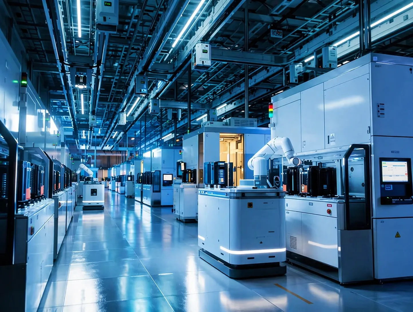
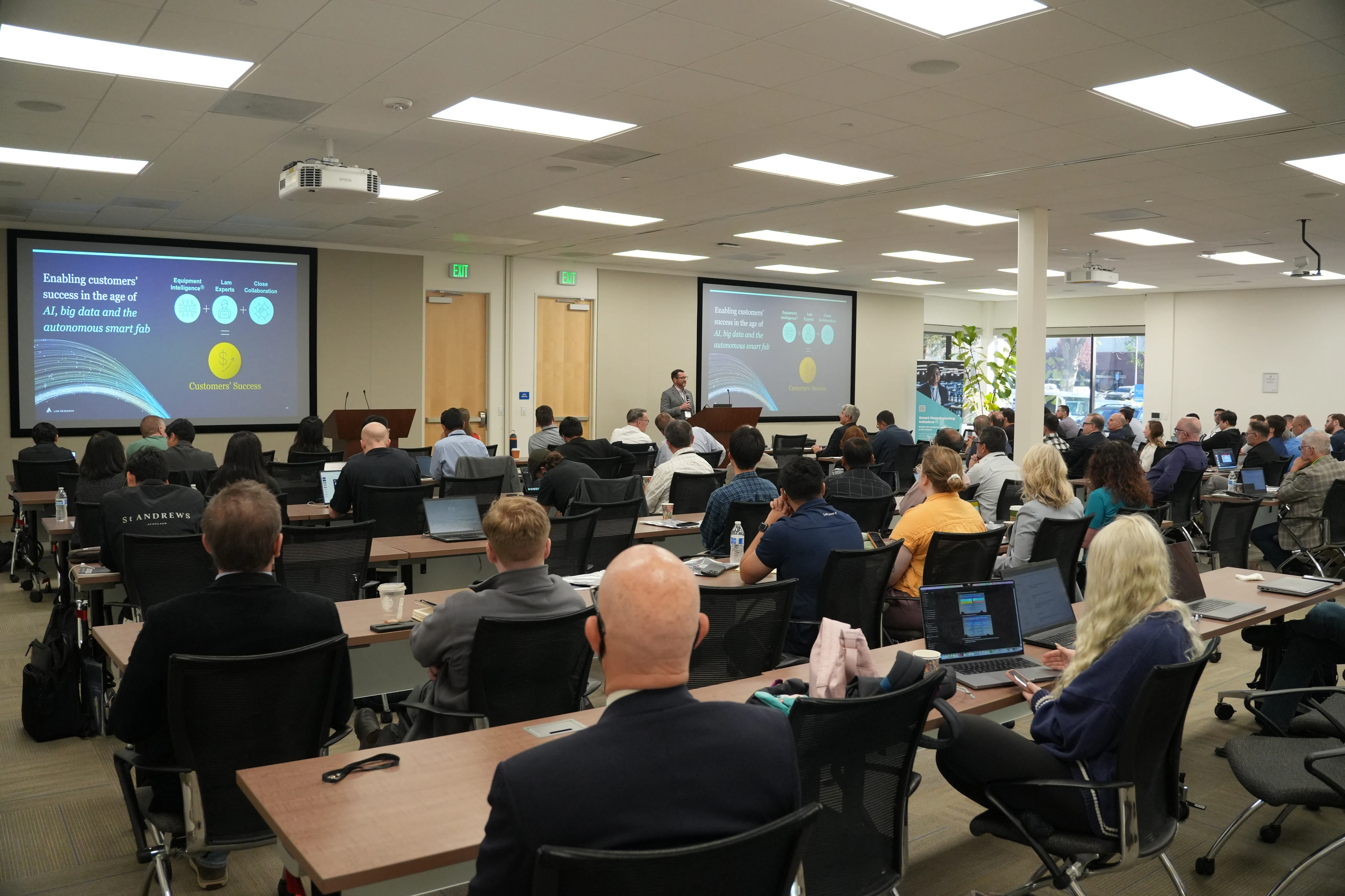
With edge AI emerging as a clear driver of smart manufacturing, SEMI hosted a two-day workshop detailing the future of this technology. The workshop, Smarter Sensors, Smarter Fabs: AI at the Edge in Semiconductor Manufacturing, was held in-person from March 18-19 in Milpitas, California. It convened industry professionals to explore how AI-driven sensors and edge intelligence are fostering scalable and resilient solutions for the next generation of semiconductor manufacturing. The workshop took place across four sessions, with each highlighting a unique edge-AI implementation area – including process control, yield enhancement, tool coordination, and predictive maintenance – and featured keynotes from leaders at Lam Research and KUKA. Didn’t get a chance to attend in person? View this workshop on demand. Session 1 - Smart Sensors and Edge Intelligence for Advanced Process Control​The semiconductor industry has always been defined by precision. However, as device architectures shrink to angstrom-scale dimensions, and as wafers become thinner and more fragile, traditional process control tools are reaching their limits. Sampled, low-frequency, univariate monitoring systems were built for an era where deviations were visible, failures were catchable later, and a handful of sensors per tool were enough to keep yield in check. Session 1 explored the latest sensor technologies, discussing how data collection at the point of production, with AI embedded directly into the tool, is becoming paramount for success. Advanced in-situ sensors were brought up as an example of this in practice. Although these sensors are generating richer signals than in the past, reaching lower latency requires AI models deployed at the edge.In addition, AI is extending into the physical world through robots that can handle various tasks autonomously. These robots are enabled by digital twins that provide simulation environments for training and validation before they ever see the fab floor. The common thread across Session 1 was the growing need for data and knowledge integration in fabs. Smart sensors must be built into AI systems, and those systems must be scalable across tools without sacrificing speed or reliability. Finally, the insights they generate must flow back into maintenance optimization and equipment health monitoring to promote a continuous cycle of learning. Session 2 - Yield Enhancement Through Edge-Driven Defect Detection and Classification​ Session 2 focused on how edge AI models, process sensors, and image data can identify yield-impacting defects earlier in the manufacturing process. As semiconductor devices lean into 3D architectures, the complexity and volume of data have outpaced the capabilities of traditional monitoring tools. Today's fabs are required to evaluate terabytes of inspection images per hour, as well as tool sensor traces that require analysis across dozens of parameters simultaneously. Each speaker approached this challenge from a different angle, yet the solutions fit together into a coherent architecture. One introduced Gaussian Process Regression, a model for assessing both predictions and uncertainties, as a statistically rigorous, data-efficient method for learning "golden trajectory" baselines for tool sensor signals. This generates actionable scores and maintenance guidance beyond standard anomaly alerts. Another speaker demonstrated the ability of deep learning models to triage multi-gigabit-per-second image streams in milliseconds. AI-based defect classification was shown to compress root cause analysis timelines from days to hours, with demonstrated gains of a 0.3% die yield recovery and 0.5–1% yield exposure prevention. Predictive metrology for RF filter frequency also assessed device performance using upstream process data, with less than 0.02% error.Lastly, a software-defined automation framework built on open standards and vendor-neutral architecture demonstrated effective workload consolidation onto a single edge platform. It was shown to be scalable across fabs without replacing legacy infrastructure.These presentations stressed the importance of measurement and action in real-time at the tool level. Gathering information as early as possible, using AI to triage and classify, and feeding insights back into process control and maintenance workflows, allows for a continuous cycle of improvement.Session 3 - Autonomous Work in Process Movement: Robots, Sensors, and Edge AI Coordination​The "lights out" factory is shifting from an aspiration to a concrete, engineering roadmap. To fully realize this, each presentation in Session 3 highlighted the importance of supplementing human-dependent workflows with AI systems that can act in real-time. This shift will require a mix of deep reinforcement learning and AI-based perception approaches. Currently, deep reinforcement learning is training agents to discover new routing strategies that optimize yield, equipment effectiveness, cycle time, and queue-time compliance – including joint front and back-end-of-line coordination for advanced packaging. AI-based perception is also on its way to replacing manual, pre-shipment inspection checklists, demonstrating inspection time reduction by as much as 78%. To enable these improvements, presenters suggested private 5G as the foundational connectivity infrastructure. Currently, private 5G is helping eliminate dead zones and bandwidth issues that are preventing real-time machine data and connected robotics from reaching their full potential.Based on these presentations, the prevailing formula is to integrate intelligence at every level. This includes precise in-situ sensing to eliminate manual setup and measurement, edge AI models that act on data immediately, platforms that coordinate across tools without humans, and lastly, a reliable connectivity infrastructure.Session 4 - Predictive Maintenance at the Edge: From Vibration to VisionSemiconductor fabs have long operated in a state of crisis management. Fab managers spend between 40% and 70% of their time firefighting unexpected equipment failures, rather than executing planned maintenance strategies. Unplanned downtime in semiconductor manufacturing can cost up to $1 million per hour, yet the maintenance industry has been slow to move beyond reactive repairs. Fab managers need faster ways to determine issues and act on that knowledge before wafers are lost. Session 4 outlined a framework for how this transformation will happen. At the foundation, smarter sensors (vibration, acoustic, thermal, spectral, and vision) are generating the high-fidelity, multi-modal data streams that make predictive models possible. In addition, "ultra edge" AI accelerators are enabling machine learning inference to happen directly inside MEMS sensors and on-device hardware without cloud dependency. Fabs require low-latency, data-sovereign, real-time decisions that the cloud is unable to support, and the path forward requires an integrated chain of sensing, edge inference, health scoring, and maintenance scheduling. This session also made the case that irrelevant correlations and confounding variables make purely statistical AI unreliable for root cause analysis, and that causal AI models are required to give fabs actionable information. It concluded that cybersecurity concerns, soaring cloud infrastructure costs (datacenter GPU prices reaching $25,000–$50,000 each in 2025–2026), and latency requirements have made distributed, machine-local intelligence the only viable path to achieving autonomous fabs. SummaryThis workshop highlighted how edge AI, smart sensors, and advanced connectivity are transforming semiconductor manufacturing by enabling real-time process control, faster defect detection, and more autonomous operations. Across sessions, experts emphasized that integrating AI directly at the source of data is essential for improving yield, reducing downtime, and building scalable, resilient “smart fabs.”Learn more by registering for this workshop on demand, or view the recap videos on LinkedIn. Day 1 recap Day 2 recap The SEMI Manufacturing Coalitions include Smart Manufacturing, Fab Owners Alliance (FOA), MEMS and Sensors Industry Group (MSIG), Advanced Packaging Heterogeneous Integration (APHI) and Semiconductor Components, Instruments, and Subsystems (SCIS).Anshu Bahadur leads the Smart Manufacturing Initiative, Karim Somani leads the Fab Owners Alliance (FOA), and Paul Carey leads the MEMS and Sensors Industry Group (MSIG), all of which are part of the Technology Coalitions at SEMI.
Read More
Today’s post is the last of four Q A-style feature posts based on presentations during SEMICON West 2025’s “The Convergence of Semiconductor Manufacturing and Design” organized by the ESD Alliance (ESDA).Bob Smith interviewed Joe Kwan, Director of Product Management from Siemens EDA, about his presentation, “3D Design Brings Multi-physics Requirements While Manufacturing Yield Improvements Require Digital Twin Modeling and Ingesting Design Data.” They covered a range of topics from partner collaboration and integrated design flows to digital twins, AI and more.Smith: How does Siemens EDA define collaboration between design and manufacturing? What does that look like?Kwan: Manufacturers and designers have been cooperating for a long time. The most familiar example is the design rule check (DRC) rule deck provided by the foundry to the design team. It enforces designers to adhere to the layout rules that must be followed for a design to be manufacturable. What’s different now are new problems arising from the latest advances in technologies. Close collaboration is needed between the design team and foundry to identify and share data necessary for a successful final product. Foundries are challenged to encapsulate information that provides design teams with critical information for success without divulging proprietary data.Smith: Can you elaborate with a few examples of what technologies you are referring to that are driving these new collaborations?Kwan: Sure. A great example is the industry’s move from monolithic single chip solutions to chiplet-based solutions that require 2.5D, 3DICs, heterogeneous integration and the like. These approaches require multi-physics simulations to verify physical phenomena in ways that were not necessary when previously focusing on just a single chip design. Thermal, electrical and stress are not independent variables anymore.Design teams need to understand how these effects come in to play with functionality, performance and other design specifications. Most important, they need to be aware of factors that could cause the chip or system to fail. To do this, close collaboration between all parties involved (design team, foundry and packaging) is required so designers know what to look for in their analyses and what to avoid. It adds a whole new layer of complexity necessary for getting to the finish line.Smith: I imagine some scenarios that fit into what you are talking about. For example, if the design includes stacked die, the team will need to be concerned about heat distribution and potential hot spots in the stack. Kwan: That is a good example. Heating problems cannot be overlooked. How does the heat escape from the stack? What is the thermal profile across the stack from the die on the top all the way through to the bottom of the stack. Is there a sufficient pathway for heat to get out? We can do rough estimates early on to see if putting this die on top of this other one, is it going to work? Or be reliable? Back of the envelope calculations might show that the dies need to be positioned differently or even designed differently. Smith: What can be done to improve design success?Kwan: This is where collaboration comes in. The product owner should establish a cross-domain team of experts from chip design, package engineering and process engineering. The product spec and design decision trade-offs must be evaluated against impact to all domains.EDA also plays a critical role. EDA is the link between designers, packaging and manufacturing. We hear and capture concerns from designers and package engineers. We prototype solutions, collaborating with packaging and IC manufacturers to encapsulate requirements for successful production.Smith: At SEMICON West, we also talked about how design data can help foundries during the manufacturing flow.Kwan: Yes, going back to our discussion at SEMICON West, I spoke about that important topic, which is embodying design data into the manufacturing platform in the context of a digital twin for virtual metrology.In an ideal world, we would measure everything. If we could do that, we would have all the data needed to make perfect manufacturing decisions. But it would be extremely expensive. What we can do instead is apply AI virtual metrology. We collect the usual sparse metrology and then combine design data to train a predictive engine. The result is the ability to accurately predict where metrology was not collected.With traditional process-of-record, foundries run a qualification wafer every 10 or so wafers. That’s very expensive. With virtual metrology, we can predict when drift becomes significant enough to blow up a wafer and you can intervene to restore individual nominal tool performance.Smith: Engineers are writing their own agents to automate parts of the design flow such as analyzing the outputs of simulations.Kwan: We see a lot of interest in AI and Agentic AI. There is a lot of potential to improve engineering productivity. But as we race to develop Agentic AI flows, we must also approach this in a rigorous manner that cross-checks to ensure accurate and robust results.About Joe Kwan Joe Kwan is the Product Director for Calibre AI/ML Fab Solutions at Siemens EDA. He has more than 30 years of experience in the EDA semiconductor industry. He previously worked at VLSI Technology Inc, COMPASS Design Automation, Silicon Access Networks and Virtual Silicon. Kwan received a Master of Science degree in Electrical Engineering from Stanford University and a Bachelor of Science degree in Computer Science from the University of California, Berkeley. Robert (Bob) Smith is an independent consultant who has been involved directly in multiple roles in the EDA industry over the past 38 years. His career experience spans analog engineering, marketing, sales, business and strategy development and others including numerous c-suite roles. He holds a Master of Science degree in Electrical Engineering from Stanford University.
Read More
Lu Dai, Vice President of Technical Standards at Qualcomm, presented “Converging Chip Design and Manufacturing in the Era of High Integration” at SEMICON West in October 2025, offering an insightful look at how design and manufacturing are collaborating effectively.I had an opportunity to talk at length with Dai and asked him to define collaboration. His thoughtful answers, perspective on industry trends and what it will take for a seamless automated flow between design and manufacturing made for a great discussion.In addition to his role at Qualcomm, Dai, who lives in San Diego, is Chairman of Accellera Systems Initiative, Chairman of RISC-V International and Director of Silicon Integration Initiative (Si2).Smith: Qualcomm is a fabless company. How do you define what collaboration is between design and manufacturing? Dai: When we talk about design and manufacturing collaboration, we need to consider how a design is optimized for a certain manufacturing process. For example, will an advanced manufacturing capability help designers simplify designs or allow them to bypass traditional actions?I compare it to the way software was optimized to hardware because of hardware limitations. We had to make sure the C code was compact and that the variable types we specified wouldn’t waste memory. We also had to write the code in a certain sequence to speed up the execution of the code. As hardware capability grows, we can write dirty code and it isn’t as critical. We understand the manufacturing process capability. That allows us to be more flexible about where to focus the chip design effort based on needs for power, performance, area, and schedule. We want to make sure we know the chip size and how big the silicon space is for certain features. For example, low power is often a key feature of today's designs. As manufacturing process nodes improve, power goes down and area shrinks. We can therefore focus more on optimizing performance.This is the kind of collaboration we use with foundries. Libraries need to be optimized for the design and tweaked for yield. This collaboration is critical for foundries pushing leading-edge nodes in the design house—they have to work closely with the design team.Smith: And how about collaboration with packaging suppliers? Dai: I'm not a packaging expert. Traditionally, packaging is one of the important steps and even more so because of the push toward the use of chiplets. Packaging becomes really important when dealing with multi-chiplet types of design. Traditionally, IP vendors sell a license to use the register transfer level (RTL) code, which is subject to IP theft. With a chiplet approach, they sell a netlist, which often becomes a hard coded chip as a bundled service instead of a single IP. The subsystem sales approach makes more money, creating another opportunity or a new landscape. SoC companies may get into the IP business and conversely, IP companies are getting into the SoC business by selling the bundled subsystem. Smith: The margins are getting blurred. It sounds like there is collaboration and it’s between designers, but also the foundries, process and the packaging.Dai: And partially between EDA tools because both the design side and the manufacturing side are speaking two different languages. EDA is somewhere in between, helping the translation.Smith: What are the trends and challenges that make it hard or even prevent a fully integrated flow?Dai: The extremely high costs of doing the implementation for an advanced node, especially for the first tape out. If we are the first to use the newest node, we know there is a tremendous benefit in the long run. But we are also the pioneers that have to work out the tough challenges. Few companies have the technical capability and deep financial resources to be the pioneers for a new process node. We’re starting to see high-flying semiconductor companies use leading-edge nodes. On the design side, they are challenged and trying to run faster by adopting a newer node. Cost is probably the biggest challenge for this collaboration. If their margins get challenged or they need to be a little bit more careful, they adapt by becoming fast followers.Another challenge comes from more specialized designs. There has been a long period where general-purpose chips are used for many different applications. But, we are now seeing designers increasingly focus on more specialized chips with custom designs.Custom IP and ASICs are becoming trendy. Designers are trying to figure out how to make a general baseline and then differentiate on certain IP and the best possible manufacturing process for the application. Doing a custom chip on an advanced node is quite expensive. We may be challenged if we don’t have sufficient data to clean up a process because every chip and process combination is unique. Lessons learned from this chip may or may not apply to everyone, while a general-purpose design tends to be a good baseline for lessons learned.Smith: How do you envision an integrated automated flow between design and manufacturing? Dai: In today's environment, we would like an RTL design to be fully portable to any kind of manufacturing process or foundry. Based on our architectural and business, we could then pick and choose the fab and the process. How do we port a design into a new process? That's difficult because we need to consider special constraints required by the new process that didn’t apply to the previous process. There's also the reverse case for porting a new design into an old process.Let’s say we have a chip designed for a 3-nanometer process and we want to port it back to a 28-nanometer process. Why would we want to do this? Imagine a COVID type of situation—a supply chain constraint and/or a geopolitical flare up with no access to the advanced fab, but an older local fab is still available. In this case, we need the chip for the feature it provides. Perhaps a car needs that chip and it was designed to be produced in a three-nanometer process but is suddenly unavailable. A 28-nanometer chip that runs at half of the speed might do the job for a few years. Unfortunately, this is somewhat wishful thinking because of the challenge of the flow. We didn’t think about it but we have to do it now and need to consider whether we have sufficient time to work out the challenges.Smith: How do you make that decision for making chiplets? Dai: Porting to another process is not a small job. It's labor intensive going from a same design in one process to another process.The project lead presents a process porting non-recurring engineering (NRE) cost budget to management. The questions span resources and time needed that boil down to how much money will need to be invested to achieve the porting. It should be simple. It’s not. It’s a lot of work.For many companies, the strategy is to offload the porting to a low-cost geographical team with a cheaper NRE that matches management expectations for the costs of process porting. History often shows that the company is not reducing that much time and manpower by offloading the porting. Smith: What about the EDA tool side? Is there typically a team from the EDA vendor? Dai: For advanced nodes, we involve the EDA and in-house EDA experts when certain parts of our design don't work out as expected.Back-end tools need experts involved in the debugging. And if we don't have an in-house expert, we need our EDA vendors to send engineers to work on the project.Smith: I have a generic question about AI. We talked about reporting. Where would it fit in collaboration?Dai: Sooner or later, we're going to be asked for a proper supply chain tracking or hardware bill of materials (BOM). Conceptually easy, but difficult in practice because it goes from logic design to physical design all the way to manufacturing. How do we carry that type of information through each step with EDA tool providers and manufacturing equipment providers? Their credentials need to be registered and they can’t alter any of the existing flow credentials.Supply chain tracking can ensure that if there's any kind of natural disaster or geopolitical issues, the hardware BOM is properly categorized, and the chip can be made. Security is another reason for supply chain tracking. Collaboration between design and manufacturing is important because once a netlist is sent to the foundry, our job is to make sure it is done correctly. We wait for our silicon to come back. Then we do testing. But during manufacturing, the chip comes back and it doesn't work. How do we know if somebody tampered with it? Supply chain tracking could help.Smith: How can you know that someone didn’t tamper with a chip design after it was handed off to manufacturing? This could cause big issues for end markets such as medical, automotive, defense and aerospace applications.Dai: The solution is EDA heavy because EDA tooling can help on the traceability at every step. It’s all automated through some kind of tool. If we need to have a proper format, we need to have proper encryption. And we know when we use this tool to run it, we check to show we are using the real tool not a hacked version that doesn't have the security credentials.Smith: Will this drive supply chain tracking or drive new standards?Dai: I hope so. Once upon a time, there was an initiative by the Department of Defense to track the supply chain. It was a mandate and no one liked it. It’s much better for the industry to proactively come up with a standard for a global economy.A mandate tends to come from one government. It may be a good mandate if we do business only within one country or within a small region. What if we have to do business with another government that may not like our mandate? Say a certain part of our design stage is done in a different country and we need this level of detail. Who's doing the work and what's the tool version? Per local government rule they may not be willing to give the information to us. This might be sufficient. We don't know the details of the risk, but we know there is a risk. We could simply add to our tracking that a portion of design is done in a foreign country with foreign EDA. It's important to have an industry standard and an international standard so that we can procure our tools and the services around the world instead of being limited.Smith: How can we encourage companies and people to want to cooperate and sign on to a project like this?Dai: With lessons learned, we can go deeper. Maybe the first level is a meeting in the U.S. About Lu DaiLu Dai is Vice President of Technical Standards at Qualcomm Technologies, Inc., spearheading semiconductor standards efforts and relationships with industry organizations. Lu was previously Senior Director of Engineering and led Qualcomm’s SoC design verification team and front-end methodologies and initiatives. He was also the Design Verification Lead responsible for multiple generations of premium tier platforms at Qualcomm, including the Snapdragon 8 series and products that power the Mars Perseverance rover and Ingenuity helicopter. Prior to Qualcomm, Lu was the Design Verification Lead for Cisco’s Gigabit Switching Business Unit where he worked on multiple generations of Cat4k ASICs. Lu is the current Chair of Accellera, Chairman of the RISC-V International Board of Directors and serves on the Board of Directors at Si2. Lu holds a Master of Science degree in Electrical Engineering from Cornell, and a Bachelor of Science in Electrical Engineering and Computer Science from UC Berkeley.Robert (Bob) Smith is an independent consultant who has been involved directly in multiple roles in the EDA industry over the past 38 years. His career experience spans analog engineering, marketing, sales, business and strategy development and others including numerous c-suite roles. He holds a Master of Science degree in Electrical Engineering from Stanford University.
Read More
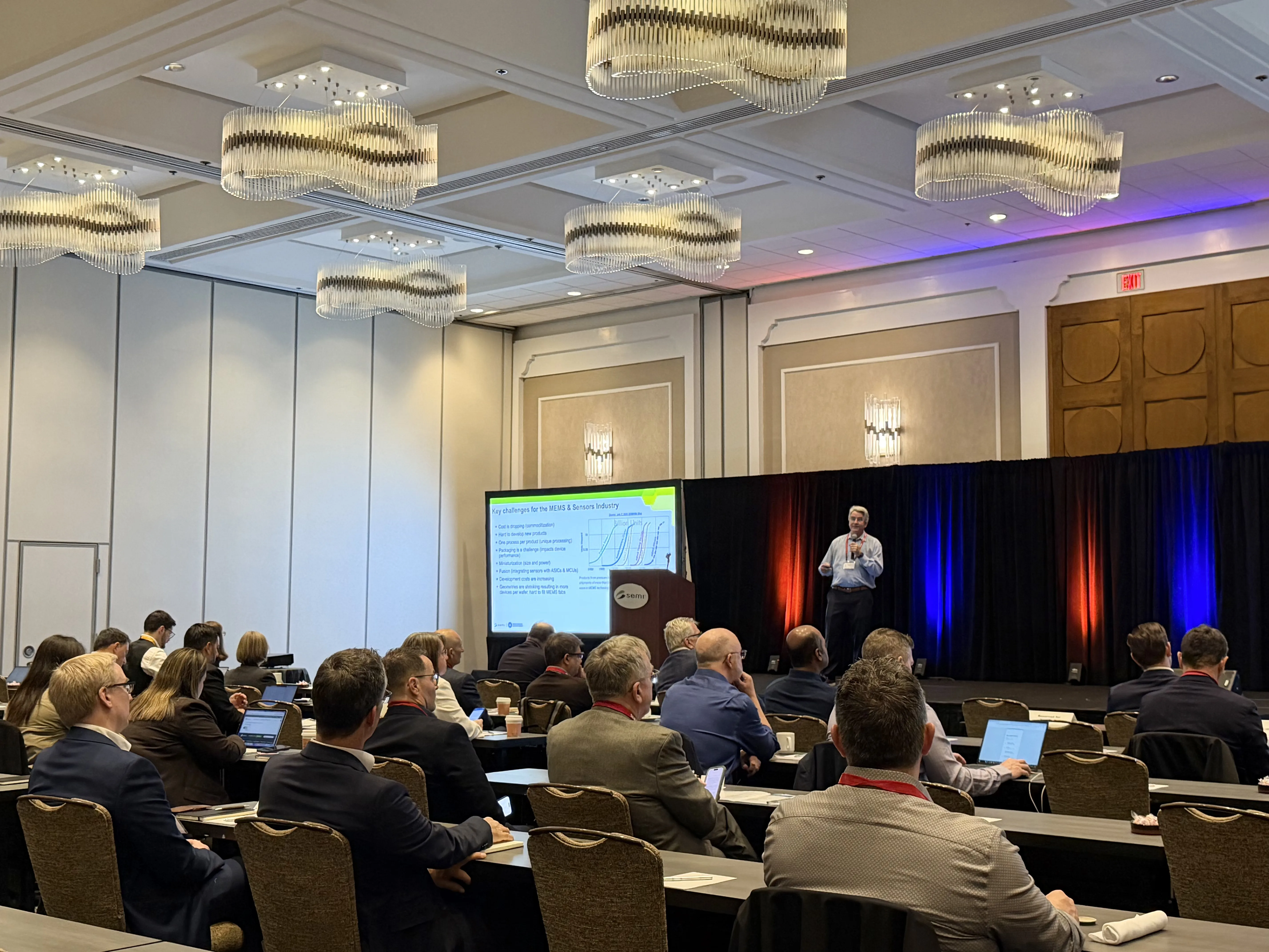
The artificial intelligence revolution has a dirty little secret: for all its "brain" power, AI and autonomy are hopeless without the hardware that connects them to the physical world. Today’s semiconductor-related blockbuster tech topics like autonomous humanoid robots, Edge AI, self-driving cars, and lights-out fabs all depend on a variety of sensing modalities and enabling technologies (from MEMS to photonic and others). The 2026 MEMS Sensors Executive Congress (MSEC) gathered industry leaders to discuss how sensors continue to evolve from simple sensing components to the essential “eyes and ears” of a global, AI-driven transformation.The Sensor Industry is ShiftingMarcellino Gemelli of Bosch Sensortec took a retrospective approach during the Leadership Roundtable starting with the statement “to understand where we are going, we have to look at where we’ve been.” While logic and memory chips scaled rapidly, sensors faced a different reality:Commoditization: Rapid price erosion in high-volume markets like mobile.The "One Process, One Product" Curse: Unlike standard CMOS, every new MEMS device historically required a unique manufacturing flow which results in high development costs.Hard to fill MEMS Fabs: Geometries are shrinking resulting in more devices per waferPackaging: A challenge because it directly impacts device performanceSensor Fusion: Integrating sensor components with ASICs and MCUs to create smart sensorsAccording to Maximize Market Research, the global sensor market is predicted to have an 8.7% CAGR from 2024 through 2030. There is a fundamental realization about sensors: the next stage of autonomous manufacturing and intelligent systems cannot exist without high-fidelity, real-time sensor data from the edge. This was a common theme throughout MSEC. Data presented at MSEC by Pierre-Marie Visse of Yole Group shows the global MEMS market is projected to grow more slowly with a 3.7% CAGR over the same time frame, with higher growth predicted for automotive, industrial, and medical applications.The Leadership Roundtable, featuring executives from Bosch, Infineon, STMicroelectronics, and Rogue Valley Microdevices, highlighted the strategic roadmaps that will define the next decade, echoed by others during other technical presentations:The Edge of Perception: AI is pushing sensing technologies to process data within the sensor itself and not in the cloud, reducing latency and power consumption while improving privacy.Autonomous Manufacturing: Leaders like John Behnke (INFICON) and Edvard Kälvesten (Silex) mapped out the path toward “Autonomous Fabs,” where sensors allow tools to communicate and self-optimize with minimal human intervention.Emerging Modalities: Beyond traditional motion and pressure sensing, MSEC spotlighted the rise of Quantum sensors for resilient navigation and Photonics combined with MEMS for ultra-precise inertial sensing.From “Parts” to “Interfaces”A recurring theme throughout the congress was the death of the "sensor as a part" mentality. In his keynote, Kurt Busch (Syntiant) argued that sensors plus AI models are becoming the default interface layer for products.“The next-generation interface is not a screen. It is the physical world, captured by sensors, interpreted by models, and delivered through natural interactions,” said Busch.This shift is visible in the rapid adoption of Edge AI integration, the development of humanoid robots, autonomous drones and vehicles, and AI enabled smart glasses—rewriting what the human machine interface looks like.Conclusion: Sensorizing the FutureWe are no longer just building devices; we are building an “industrial AI operating system” that connects the digital and physical world. This all starts with sensors. By 2030, the most valuable AI won't just be the one with the biggest brain, it will be the one with the best senses.If you are a leader in the field of MEMS Sensors, let your voice move the industry needle by becoming a SEMI and MEMS Sensors Industry Group (MSIG) member company and getting involved with MSIG. MSIG will be hosting the MEMS Sensors Technical Congress (MSTC) on September 16-17 at SEMI HQ in Milpitas, CA. Engineers and technical executives will dive deep into new technology and processes that advance the sensor industry. To learn more or to be a part of the fascinating world of MEMS Sensors visit the SEMI MSIG website.Paul Carey is Director, MSIG at SEMI. Rafael Tudela is Senior Technical Marketing Manager at SEMI.
Read More
The rapid growth of AI has created a surge in the global energy consumption at a rate never seen before. Today, data centers account for approximately 415 terawatt-hours (TWh) of electricity globally. To put this into perspective, the annual energy consumption of the United Kingdom in 2023 measured at 309 TWh. The International Energy Agency (IEA) projects data centers’ energy consumption will more than double to nearly 945 TWh by 2030 [1]. A single generative AI query can consume up to ten times the power of a traditional search [1]. Meanwhile, data center energy usage in the U.S. is projected to leap from 4.4% to as much as 12% of the national grid by 2028 [2]. This creates a stark reality for the semiconductor industry. Traditional monolithic scaling has hit its physical and economic limits, leaving advanced packaging and heterogeneous integration to define the industry’s trajectory [3].To meet these escalating compute demands, the industry is rapidly shifting toward multi-die architectures, chiplets, and 3D stacking to decrease the amount of energy needed for advanced computing. This transition is fueling explosive growth in the advanced packaging market, which the Yole Group projects will reach $79.4 billion by 2030 [4]. However, stacking chiplets to bypass Moore’s Law exposes massive systemic bottlenecks. Engineers are now fighting interconnect parasitics, navigating complex power delivery architectures, and battling extreme thermal density.In a 3D-stacked architecture, pulling heat away from vertically integrated dies is one of the most pressing engineering challenges of our time. As compute density rises, issues like die warpage and localized thermal hotspots threaten both reliability and yield. The shift toward sustainable AI systems for energy-efficient computing requires breakthroughs in everything from hybrid bonding process flows to advanced thermal interface material (TIM) strategies and liquid cooling integration [6].These are not challenges that any single company can solve in isolation. Whether you are a foundry, OSAT, material supplier, or equipment provider, overcoming these bottlenecks requires pre-competitive, industry-wide collaboration. Foundational capabilities must be built collectively before competitive differentiation occurs.This is the core mission of the SEMI Advanced Packaging and Heterogeneous Integration (APHI) Technology Coalition. By collaborating on common standards, shared research frameworks, cross-vendor interoperability models, and collective technology roadmap congruency, APHI is actively dismantling the barriers to next-generation computing.The APHI community is already tackling these issues head-on. Monthly chapter meetings identify and address these and other issues facing heterogeneous integration. The most recent chapter meetings showcased in depth review of these challenges. Jonathan Abdilla from BESI detailed the technical challenges and collaborative research required for global hybrid bonding process flows. Similarly, Dr. Jie Geng from Indium Corporation led a deep dive into crucial TIM strategies for AI and HPC, exploring hybrid stacking evaluation methods and liquid cooling options to combat GPU die warpage.The future of advanced manufacturing will be defined by how effectively we manage power and heat in heterogeneous systems. We invite you to join this critical conversation at the upcoming SEMIEXPO Heartland (April 29-30 in Detroit, MI) Day 2 will feature dedicated sessions on Thermal Management Power Delivery in Advanced Packaging: From TIMs to Warpage Control, as well as strategies for securing the advanced packaging supply chain.To help shape the standards and shared roadmaps that will power the AI revolution, explore our initiatives and get involved with SEMI Advanced Packaging and Heterogeneous Integration (APHI) Technology Coalition.Rafael Tudela is Senior Technical Marketing Manager at SEMI References[1] International Energy Agency (IEA). (2024). Energy and AI Report. [2] U.S. Department of Energy (DOE) Lawrence Berkeley National Laboratory (LBNL). (2024). Report on U.S. Data Center Electricity Demand and Grid Impact.[3] Semiconductor Packaging News. Advanced Packaging and Heterogeneous Integration. Retrieved from: https://www.semiconductorpackagingnews.com/articles/92402.html [4] Yole Group. (2025). Status of the Advanced Packaging Industry 2025.
Read More
The semiconductor industry is hitting a structural inflection point: explosive AI‑driven demand, rapidly rising manufacturing complexity, and stringent sustainability expectations are converging at once. In this context, edge AI deployed directly on tools, sensors, and local controllers, is shifting from experimental to essential, particularly in fabs where milliseconds matter. SEMI’s timely workshop, Smarter Sensors, Smarter Fabs: AI at the Edge in Semiconductor Manufacturing, taking place March 18–19, 2026 in Milpitas, CA, will address this important topic.From sparse sensing to dense instrumentationTwo decades ago, most process tools relied on dozens of sensors per chamber. Today, leading etch, deposition, CMP, and lithography systems routinely integrate hundreds of sensing channels spanning pressure, flow, RF power, optical endpoint, vibration, and chemistry. At 3 nm and 2 nm, process windows are so tight that yield hinges on multivariate understanding of chamber conditions and tool state rather than a few independent alarms. Sensor proliferation has turned fabs into rich data environments—but also exposed the limits of traditional, centrally managed control.Why edge AI is displacing cloud‑only controlConventional architectures push heavy analytics to centralized servers or the cloud, with supervisory systems periodically updating recipes, setpoints, or dispatch rules. Across manufacturing, measured cloud round‑trip times commonly range from 800 to 2,400 ms, whereas edge systems co-located with equipment can respond in 15–45 ms, roughly 50–160× faster. For safety‑ and yield‑critical loops in semiconductor manufacturing, that latency gap is often unacceptable.At the same time, new generations of low‑power neural processing units (NPUs) and edge accelerators deliver tens of trillions of operations per second (TOPS) at single‑digit watt budgets, making always‑on inference viable inside tools, cameras, and controllers. The result is a decisive move toward edge‑native architectures: models execute where data is produced, while cloud resources are reserved for retraining and fleet‑wide learning.Edge AI on the line: control, inspection, and maintenanceIn process control, edge AI is enabling a shift from univariate threshold checks to multivariate models that understand the joint dynamics of sensor streams. Platforms today embed deep‑learning and statistical models directly at or near the tool, performing real‑time endpoint prediction and anomaly detection from high‑dimensional time series. Similar approaches are emerging in lithography and CMP, where local inference helps keep focus, overlay, and removal rate within spec before wafers drift out of control.Inspection and logistics are undergoing a similar transformation. Vision systems with embedded NPUs classify defects at line speed, often above 100 parts per minute, eliminating the need to ship large image volumes to a central cluster. Robots and autonomous mobile robots (AMRs) use local intelligence for short‑horizon planning and collision avoidance, while higher‑level systems focus on global scheduling and optimization.Predictive maintenance is one of the most mature applications: vibration, acoustic, temperature, and pressure data are analyzed locally to detect anomaly signatures hours or days before conventional thresholds trip. Reported benefits include reductions in unplanned downtime, longer component life, and lower maintenance costs when these models are integrated into manufacturing execution systems (MES) and maintenance workflows.Digital twins and agentic AI on top of edge dataDigital twins build on this sensing and edge‑analytics foundation. By maintaining virtual, live‑updated models of tools, lines, and entire fabs, they enable scenario testing, debottlenecking, and root‑cause analysis without putting WIP at risk. Vendors and early adopters report that such twins can shorten process‑node ramps and facility bring‑up by enabling thousands of “what‑if” experiments before physical changes are made.​Agentic AI is now emerging as the orchestration layer above these twins. In semiconductor case studies, agents connected to MES, advanced process control (APC), and planning systems have delivered double‑digit improvements in throughput, cycle time, and tool utilization by autonomously adjusting routing, batch sizes, and scheduling in response to live fab conditions. Other agents mine unstructured engineering notes and fault reports to accelerate root‑cause analysis, turning hard‑won lessons into repeatable, codified behavior.Sustainability as a first‑class requirementSustainability pressures are reinforcing this stack. Semiconductor manufacturing is energy‑ and resource‑intensive, and regulators and customers alike are demanding more transparency and improvement. Edge‑connected monitoring of energy, utilities, and emissions has already helped some fabs cut energy‑related costs by around 20 percent through tighter control of HVAC, process gases, and idle modes. Research initiatives such as imec’s Sustainable Semiconductor Technologies and Systems (SSTS) program are using virtual fab methods and detailed life‑cycle assessment to guide process and equipment choices for lower environmental impact.Strategic takeaways and where to learn moreThe trajectory is clear: fabs that combine dense sensing, edge AI, digital twins, and agentic AI are building toward continuously learning, self‑optimizing operations. Architectures will need to be edge‑first rather than cloud‑only. Simply adding sensors without local intelligence will not deliver competitive advantage, and environmental KPIs are likely to be optimized with the same rigor as yield and cycle time.For practitioners who want to translate these trends into roadmaps, the Smarter Sensors, Smarter Fabs: AI at the Edge in Semiconductor Manufacturing” workshop (March 18–19, 2026, Milpitas, CA) spearheaded by the SEMI Manufacturing Coalitions* will bring together experts in sensing, edge architectures, digital twins, and agentic AI to share concrete deployments and architectures tailored to semiconductor fabs.*The SEMI Manufacturing Coalitions include Smart Manufacturing, Fab Owners Alliance (FOA) MEMS and Sensors Industry Group (MSIG), Advanced Packaging Heterogenous Integration (APHI) and Semiconductor Components, Instruments, and Subsystems (SCIS). Anshu Bahadur is Senior Program Manager, Technology Communities at SEMI. Mark da Silva is Senior Director, Manufacturing Coalitions at SEMI.
Read More
Edge AI is a fundamental technology for applications that require real-time decision-making. Contrary to cloud-based AI solutions that specialize in large and complex tasks, edge AI is embedded directly into local devices, allowing for lower-latency decision-making for less bandwidth consumption. These properties are essential for advancing technologies like 6G, autonomous vehicles, industrial IoT solutions, and more. However, edge AI can’t be achieved with traditional silicon because it requires more efficient thermal management, higher performance, and lower power than silicon can deliver. To address these limitations, the Silicon-on-Insulator (SOI) technology platform offers a path forward. SOI is a layered silicon substrate technology with a silicon device layer on top, an insulating silicon dioxide layer in the middle, and a thick silicon base at the bottom. This structure disconnects devices from the bulk substrate, enabling major performance improvements for faster and more power-efficient ICs and photonics devices. In addition, FD, or fully depleted SOI (FD-SOI), is a subcategory of SOI that offers even higher performance and lower power usage.According to Michaël Tchagaspanian, Executive Vice President of Technology Strategic Partnerships at CEA-Leti, SOI is not just an alternative material. Instead, it’s a foundational technology that’s crucial for advancing the next wave of edge AI innovation. Therefore, to accelerate its advancement, CEA-Leti is combining its four decades of pioneering research with the cooperative efforts of the SEMI SOI Industry Consortium.CEA-Leti’s HistoryFor nearly 50 years, CEA-Leti has been at the forefront of SOI leadership. The company began in 1980 with its research into radiation-hardened electronics, which led to breakthroughs that enabled the Smart Cut™ process. Smart Cut ultimately served as the foundation for enabling SOI wafers to become a commercially viable global standard.This legacy also paved the way for much of the cutting-edge R D of today, including the FD-SOI Next Generation 10-7 nm program. This effort leverages flexible back-biasing to allow dynamic control over power consumption, leading to substantial efficiency gains.Tackling Tomorrow’s Challenges: A Sustainable FutureCEA-Leti’s deep SOI expertise allows it to address many of edge AI’s environmental challenges. To promote energy efficiency, CEA-Leti is working to advance silicon photonics while at the same time, incorporating the comprehensive PPAC-E framework across its new technology developments. The organization also works toward reducing energy through its fully integrated neural-network-on-chips technology that uses hybrid memory. This effort supports ultra-low-power, on-chip learning and inference for applications like autonomous vehicles, medical sensors, and others. Finally, CEA-Leti works to reduce greenhouse gases through its involvement in the GENESIS project, plus its ongoing efforts in eco-design and lifecycle analysis. The SOI Industry Consortium: Accelerating Industrial AdoptionAs part of its partnership, the SOI Industry Consortium works to ensure that CEA-Leti’s lab innovations can be seamlessly integrated into global production. This "lab-to-fab" model can be seen in the volume production of FD-SOI transistors from leading companies like STMicroelectronics and GlobalFoundries. The Consortium helps achieve volume production through its three-part approach: Secure the supply chain, reduce SOI adoption barriers, and close the specialized skills gap. To promote a healthy supply chain, the Consortium offers a platform that brings lab-to-fab solutions for SOI wafers. This is achieved through leading-edge development capabilities at CEA-LETI, Soitec and its Foundry manufacturing partners, with additional support from leading wafer suppliers like Shin-Etsu, GlobalWafers and Okmetic.It lowers SOI adoption barriers by collaborating with EDA leaders to standardize design tools and methodologies, ensuring robust proven design flows fully leveraging SOI technology.Finally, the Consortium supports training initiatives that address the SOI industry’s specialized skills gap. Partners like Synopsys also provide extensive training options, equipping engineers with the expertise to master SOI designs. SOI is helping the innovations of tomorrow become a practical reality. CEA-Leti’s leadership, combined with the global reach of the SOI Industry Consortium, allows the SOI ecosystem to optimize for low-power and sustainability while driving the next generation of high-performance systems. Gity Samadi is Senior Director of R D at SEMI.
Read More
Aki Fujimura has been at the forefront of chip design innovations from the beginning of his career and his technology leadership continues today. He serves as Chairman and CEO of D2S, co-founder of the eBeam Initiative, President of BACUS, and a Governing Council member of the ESD Alliance, a SEMI Technology Community. At Tangent (now Cadence), Fujimura and Steve Teig (a chip designer for the last 20 years and now Vice President and Distinguished Engineer at Amazon) built the first commercial over-the-cell routing system dedicated to fully synchronous designs with timing assurance and automated test-scan insertion. Fujimura and Tom Kronmiller developed LEF/DEF for efficient representation of Manhattan routing, both used as standards in the automated place and route (P R) flow to this day. He again teamed with Teig and Kronmiller to develop the X Architecture, an interconnect architecture based on the pervasive use of 45o diagonal routing. I was thinking about his background as I called him to chat about his evolution from chip design before focusing on chip manufacturing via eBeam technology at D2S.Smith: Let’s talk about your journey from focusing on how to do physical design of chips to chip manufacturing. How did this happen?Fujimura: GPUs weren’t a thing until late 1990s. With CPUs, Manhattan design was the obvious choice for computational efficiency. Largely gridded metal n that went up and down, and metal n+1 that went left and right with vias to connect the line segments were how all automated layout worked. PCB routing and packaging (even back then) used diagonal routing and even curved routing. But chip P R was all Manhattan. That was still true when we worked on the X Architecture at Simplex Solutions (now Cadence). ATi (now inside AMD), NVIDIA and several other GPU companies started in the late 1980s to 1990s, but they were targeting video and gaming more than scientific computing at the time. It’s when Teig came up with the idea for the X Architecture that he wanted to know if 60-degree routing was possible “because a hexagon tessellates a plane.” A good question. I set out to try to find out what the actual limits were in manufacturing that create the limitation to Manhattan shapes. I got introduced to the late Bill Arnold of ASML, who then introduced me to a lot of people in manufacturing who helped me get the answer. Naoya Hayashi of DNP was instrumental in helping me understand that mask making is where the limit exists. Hayashi-san kindly explained to me about the two mask writers. I had to dig around a lot more to make sure that that was the only barrier, but that’s how I came to understand that before masks, everything is data, and after masks, everything is physical. Mask making is the key that enables 45 degrees, but not 60 degrees. The lessons I learned then are still very important to me today. That’s when I saw and appreciated the opportunity there is for software for semiconductor manufacturing.Smith: But you still couldn’t use GPUs for the X Architecture work?Fujimura: Right. Way too early. The idea that GPU-accelerated gaming machines can be connected together to do video editing, or that large scientific simulations can be done on a connected set of gaming machines, was being explored in the 1990s already. It was only 20 years ago (2006) when Jensen Huang announced his bet with the CUDA software stack for general purpose GPUs (GP GPUs) for nodes in racks of CPUs, GPUs, memory and communication to create the modern scientific computer. Six years later in 2012, AlexNet won the ImageNet Large Scale Visual Recognition Challenge (ILSVRC) with CUDA, and the rest is history. But no, we didn’t use GPUs at Simplex. But we did help design GPUs, including with the X Architecture.Editor’s Note: ILSVRC evaluates algorithms for object detection and image classification at large scale. Smith: Now, everything you do at D2S is with GPU acceleration. When and how did that change come about?Fujimura: It was back in 2009, two years after D2S was founded. An extraordinary engineer, Harold Zable, noticed that simulation-based manipulation (rather than rules-based manipulation) of mask shapes, both for wafer manufacturing and for mask manufacturing, would be the ideal application for GPU acceleration. Fast-Fourier Transforms (needed for lithography simulation and optical proximity correction (OPC)/inverse lithography technology (ILT)) and Gaussian manipulations (needed for eBeam mask simulation and mask process correction (MPC) are nearly “free” in terms of compute time on GPUs. You still have to get the data in and out efficiently, but you can do pretty sophisticated computing without much overhead. At the same time, multi-beam based eBeam writing was getting momentum, first in wafer direct write applications. In 2007, at the BACUS conference in Monterey, Calif., IMS—then a well-respected research organization in Vienna—published a paper saying that multi-beam for mask writing is what they’d like to do. The wafer market is much bigger, but this technology is more suited for mask writing, where write times are measured in hours per mask. “Wafers Per Hour” is the measure in wafer manufacturing, so mask writing gets to flip the division. We were looking at a mask design and mask manufacturing world that should be doing simulation-based manipulation rather than rule-based. That’s better with GPUs. On top of that, maybe the world is going to go to multi-beam writing, going away from four decades of variable-shaped beam (VSB) writing. And I knew from the X Architecture experience that VSB was the only thing in the eco-structure that restricted mask shapes to be Manhattan or 45 degrees. In fact, with multi-beam, any curvilinear shape within the limits of resolution of a given pixel size can be freely written on the mask. The only barrier then to having curvilinear masks would be the software stack and trying to compute it with CPUs only. We knew GPU acceleration was the answer. Smith: Was it just totally an accident that multi-beam and GP GPUs happened at the same time?Fujimura: Yeah, it was. However, just as when multiple people simultaneously invent the same thing without knowing about each other, the environment and times in which we live have a lot to do with this. So, I guess, it’s not really just “luck.” But GP GPUs in 2006 and IMS Multibeam in 2007, I think that’s luck.Anyway, D2S became the GPU-acceleration partner for the semiconductor manufacturing industry and decided to work only on things that can be accelerated by GPUs in 2012.Smith: What trends do you see going forward in the next three to five years?Fujimura: A move toward curvilinear mask features, as well as an increased interest in curvilinear wafer targets as designers become aware that the manufacturing side has established a solid path for curvilinear mask shapes. We’re leaving a lot of margin on the table to accommodate gridded Manhattan assumptions, and that’s really no longer necessary from a manufacturing standpoint. I think electronic design automation (EDA) should be working on enabling curvilinear designs, because the door is open for the design world to explore curvilinear chip design and to reap compelling benefits in terms of power/performance and reliability.Editor’s Note: While Manhattan geometries are rectilinear shapes aligned to vertical and horizontal axes, curvilinear design introduces smooth, continuous curves into layouts and masks, leveraging advanced computational lithography and mask-writing technologies. This improves pattern fidelity, electrical performance and manufacturability at advanced technology nodes.About Aki FujimuraAki Fujimura is chairman and CEO of D2S, Inc., and managing company sponsor of the eBeam Initiative. Previously, Fujimura was CTO at Cadence Design Systems, President/COO and inside board member of Simplex Solutions, and VP and inside board member at Pure Software. He co-founded Tangent Systems (acquired by Cadence).Fujimura, made a SPIE fellow in 2023, serves as President of the SPIE BACUS Technical Group. He serves on the governing council of the ESD Alliance, a SEMI Technology Community. Fujimura was on the board of HLDS, RTime, Bristol, S7, and Coverity, Inc.Fujimura received his BSEE and MSEE degrees from MIT.Robert (Bob) Smith is executive director of the ESD Alliance, a SEMI Technology Community. 
Read More