downloadGroupGroupnoun_press release_995423_000000 copyGroupnoun_Feed_96767_000000Group 19noun_pictures_1817522_000000Member company iconResource item iconStore item iconGroup 19Group 19noun_Photo_2085192_000000 Copynoun_presentation_2096081_000000Group 19Group Copy 7noun_webinar_692730_000000Path
Skip to main content
Default Banner Image

Technology and Trends

AI is proliferating rapidly, fueled by ever-larger models and data sets that are expanding AI use cases and improving its accuracy. Future computing systems are now required to simultaneously deliver high performance, process large amounts of data, and use the least possible energy. The growing energy footprint of AI and the strain it places on the power grid is an increasing concern for companies and even entire countries. This could adversely impact future growth and could slow the semiconductor industry’s march towards $1 trillion in revenue, which is largely driven by AI applications.This is a formidable challenge that cannot be addressed in silos by individual companies or even industry segments. The SEMI Smart Data-AI Initiative is exploring how to overcome this challenge with collaborative and innovative system-level solutions that connect the dots across the entire AI system stack. In March 2025, we hosted a successful workshop, bringing together industry leaders across the value chain for a day of thoughtful discussions and knowledge sharing. Building on this foundation, we developed an exciting Smart Data-AI session to be held at SEMICON West in Phoenix, Arizona on October 7 from 10:30 a.m.-4:40 p.m. The “Future of Computing: Energy-Efficient Computing for AI and Beyond” forum will bring together executives and thought leaders across the entire ecosystem – including design, fabrication, interconnects, system integration, hyperscale architectures, advanced materials, and emerging technologies such as photonics and quantum. Attendees will have a unique opportunity to get strategic perspectives from these distinguished experts and learn about exciting future trends.Why Attend?Gain insights from global leaders and learn about innovative paths towards an energy-efficient computing future.Network and build cross-industry collaborations for the next wave of AI, photonics and quantum.Promote a more sustainable path for continued growth of AI to benefit humanity and the planet.Join the SEMI Smart Data-AI initiative to develop solutions and take concrete actions to reduce AI’s growing energy footprint.Support the industry in achieving its goal of reaching $1 trillion in revenue. Speaker Highlights Include:AMD • Ciena • Hewlett Packard Enterprise • IBM • Merck KGaA, Darmstadt, Germany •Microsoft • Quantum Economic Development Consortium • Rapidus • Rigetti •Siemens AG • Stanford UniversityDr. Pushkar P. Apte is the Strategic Technology Advisor and leads the Smart Data-AI Initiative at SEMI.
Read More
Digital Twins are no longer a futuristic concept in semiconductor manufacturing—they’re fast becoming the backbone of next-generation fabs. But here’s the challenge: without a robust, scalable data platform to unify, secure, and interpret the torrent of information flowing across design, manufacturing, packaging, and test, digital twins cannot deliver their transformative potential. At SEMICON West in Phoenix, Arizona on October 6, 2025 from 1–5 p.m., join us for a high-impact technical workshop that explores how advanced data platforms are fueling the next wave of innovation—enabling smarter, faster, and more precise decisions across the semiconductor lifecycle.What You’ll Learn – Gain insights on proven reference architectures for scalable data platforms, integration patterns that support digital twin ecosystems, real-world use cases from fabs and OSATs applying AI/ML at scale, best practices in managing governance and security across complex data pipelines.Modern Data Platform Architectures – Designed for speed, scale, and semiconductor precisionBreaking Down Silos – Leveraging shared ontologies and data fabrics for seamless interoperabilityAI-Enhanced Digital Twins – Real-world deployments across fabs and OSATsFederated Learning in Action – Secure, multi-party collaboration without compromising IPData Security Governance – Proven practices for high-stakes manufacturing environments Distinguished Speakers – Hear directly from leaders advancing digital twin and federated learning initiatives at the SmartUSA Institute and across the semiconductor ecosystem. Anshu Bahadur, Senior Program Manager, Technology Communities at SEMI, will open the workshop and introduce speakers who will share how they’re building these next-generation platforms and deploying them across fabs, OSATs, and the full manufacturing flow. Following individual presentations, the session will close with a panel discussion featuring these executives. Ross Kunz, Director of Technology, SmartUSA Institute (Keynote Speaker)Dr. Adam Schafer, CEO, Athinia TechnologiesDhara Vaishnaw, Head of Solution Architecture, AWSDr. Gautham Unni, Head of Solutions and Business Development, Semiconductor, AWSJonathan Holt, Senior Director, Product Management, PDF SolutionsDr. Surya Kalidindi, CEO, Multiscale TechnologiesWho Should Attend? This workshop is designed for: Data Platform Architects building the next-gen semiconductor backboneSmart Manufacturing Engineers integrating fab and test dataAI/ML Practitioners scaling models into production workflowsInnovators shaping digital twin systems for complex, high-precision manufacturing Why Attend? Because the future isn’t waiting. Digital Twins, powered by scalable data platforms, are redefining how the semiconductor industry innovates, collaborates, and competes. Don’t just keep up with the future—build it. Anshu Bahadur is Senior Program Manager, Technology Communities at SEMI
Read More
John Kibarian, CEO and co-founder of PDF Solutions and a member of the ESD Alliance (ESDA) Governing Council, will deliver a keynote during the CEO Summit at SEMICON West in October titled, “Revolutionizing Semiconductor Collaboration: The Emergence of AI-Driven Industry Platforms.” He recently shared with me a summary of what his talk will cover and his perspective on why collaboration is the key to growing the semiconductor industry to $1 trillion and how we will get there.Smith: What is the major industry evolution or dynamic that's making collaboration essential today?Kibarian: The semiconductor industry has dramatically evolved from a simple, linear process to a complex, collaborative ecosystem. Previously, everything happened at the wafer fab. Testing occurred at wafer sort, package yields were high, final testing was straightforward, and products were shipped. Collaboration was mainly between foundries and fabless customers, intensive during early qualification and test chip stages, then evolved to routine yield monitoring once production stabilized.Today's advanced packaging puts multiple chiplets into single packages, creating an explosion of test insertion points. This has driven up both test complexity and costs significantly. Front-end fabs now house the most complex machines, while test and assembly facilities, once relatively simple, now feature sophisticated system-level testers with integrated robotics. Assembly tools have become highly complex, with die-attach processes requiring increasingly tight tolerances. Success now requires collaboration across the entire chain, from system companies to equipment vendors, both for new product launches and ongoing production maintenance.Companies are adopting AI and machine learning (ML) to manage these complex production flows, whether for testing or equipment control. This demands even broader collaboration since AI requires combining data from multiple sources across foundries, fabless companies, OSATs, equipment vendors, and more, data that no single entity controls. What was once a straightforward handoff between two parties has become an intricate web of interdependent relationships requiring continuous coordination.Smith: Chiplets and chiplet-based architecture is in the news and seems to be a key solution or practical solution in response to the slowing down of Moore's Law. This demands incredible levels of collaboration and coordination across the whole value chain. Is this doable at scale where it starts to move into the mainstream?Kibarian: The semiconductor industry will need unprecedented collaboration to make chiplet manufacturing work at scale. But this can be done! Consider EUV lithography: Initially expected during the 65nm generation, it took years longer than anticipated despite being an incredibly complex technology. Extraordinary engineering was needed but it also required extensive collaboration between ASML, suppliers, customers, and the broader fabless community.If the industry achieved this level of coordination for EUV, it can do the same for chiplets. However, chiplet manufacturing will require even greater collaboration as more companies will build systems using chiplets from multiple suppliers.Today's chiplet-based systems typically source all components from one manufacturer, making standards like UCIe less critical since companies control their entire supply chain. This will change as companies increasingly use third-party components for cost-effectiveness.More and more, we will see systems using components from multiple players to get to market more cost-effectively. Consequently, future production flows will be significantly more complex, requiring coordination of substrates and base dies, third-party dies and interposers, OSAT and specialized testers with specific configurations.This orchestration must work not just for initial bring-up but for the ongoing production as well, and when reconfiguring chiplet combinations for different products, all requiring rapid, automated responses.All of that must be automated for quick reaction. Considering the complexity of the manufacturing flow, people will want to apply AI/ML to anticipate what is going on in each individual product built.Manual oversight of every chip and package during manufacturing isn't feasible at scale. Automated AI agents must handle this monitoring and quality control. Expanding this automation will require close collaboration between the manufacturing entity and engineering teams at the product companies.This will also require a different level of alignment and orchestration across all the software packages managing this complex multi-company process. The financial enterprise resource planning (ERP) systems know where material is going, what the demand is, and what the forecasts are. While separately, the manufacturing execution systems needs to know which tools are going to be available when. Most often, these manufacturing systems operate in factories the product company doesn't own. The product company’s PLM systems control the bill of materials and test flows, but these tests will be conducted at the OSAT requiring complex coordination between the software systems of multiple companies controlling different process domains. This orchestration spans organizational boundaries and must be able to take data from upstream test results and make decisions on what tests to run downstream. This is required to get the right chiplets put together into a package in an efficient manner within a short cycle time and not require a Formula 1 pit team to keep everything running.Smith: The volume of data is staggering, especially now with design data. What will it take to enable this vision, at scale, where everything's connected? Kibarian: It’s a marriage of the human establishing the bounding box within which the systems operate that employ agents to do a lot of the work on a day-to-day or hour-by-hour basis. A good example is how manufacturing execution systems (MES) connect to ERP systems to share data. When a company sets up an orchestration, it creates rules that govern how information flows between systems. These rules tell the ERP system: "To calculate costs for each process step, here's the recipe information you should use."Once these rules are in place, they work like guidelines that control daily operations. An AI agent automatically creates insights based on actual data collected from the MES and moves data between systems according to these rules. The ERP AI agent will use this data to spot when costs are rising and send alerts, to notice when production yields drop, to calculate what lower yields mean for costs, and will take action to fix problems.This same process happens between equipment suppliers and manufacturing facilities. They share data automatically based on pre-set rules, and AI helps identify issues and take corrective action. Fabs determine who can access which machines and when, what types of data can be transmitted and through which channels, and how frequently these transmissions occur. When new software or AI models are introduced to run equipment, the systems specify what virus scanning and security checks must be completed before installation.Human operators primarily configure these control systems by determining the most effective collaboration protocols. However, the day-to-day execution is handled by automated agents due to the enormous scale involved, both in terms of data volume and the sheer number of transactions that occur continuously throughout operations.A human will not go through and review that data. I'll give two examples of this. One outside of our industry and one in our industry. At our 2019 user conference, board member Marco Iansiti, a Harvard Business School professor, shared insights from his book on AI in business. He compared traditional banks with Ant Bank, Alibaba's banking arm, which was experiencing explosive growth before Chinese government intervention.Ant's AI wasn't particularly sophisticated, but its process was revolutionary. While traditional banks require customers to fill out loan applications that then go to human loan officers for review, Ant's system would automatically scrape the internet and social media to verify applicant information. Within seconds, an algorithm would approve or deny the loan.The crucial difference is that Ant could scale exponentially because its only constraint was computing power. Traditional banks need to hire more loan officers to double their business, a human bottleneck that limits growth.I invited him to speak because I believed in this principle six years ago, and I'm even more convinced now.For the semiconductor industry, to build a trillion-dollar industry with complex, integrated systems, we need to minimize human intervention in data intensive processes. Despite the trust issues between stakeholders in our sector, collaboration remains essential. The solution requires establishing systematic principles that allow AI agents to operate autonomously. This is a way forward to achieving exponential growth.The Ant Bank example perfectly illustrates what our industry needs. At PDF, we believe this approach is crucial for industry advancement. Consider this: We manage petabytes of data, yet humans only examine 5-10% of it. This shows AI's potential to handle the vast majority of operations without human oversight.The reality is that our customers build millions of chips a week, billions a year. They cannot look at every dataset. Algorithms can, AI can. We launched a product called Guided Analytics last year. An engineer spoke about it during our user group last year. Her company has a couple of thousand products. Her group could not keep track of them every day, but Guided Analytics could. When her group came in the morning, the daily report noted 90% of the chips were fine or alerts pointed to where issues are. It's a simple AI bot crawling over data and identifying where the root cause seems to be.Our industry will require more agents to scale. Those agents will span the industry, and yet we as humans need to set up the governing principles under which they can operate. That's how we're going to deal with the massive amounts of design and manufacturing data to get the velocity the industry will need, and to benefit from the AI that we create for our businesses.Notes: Kibarian’s keynote, “Revolutionizing Semiconductor Collaboration: The Emergence of AI-Driven Industry Platforms” is scheduled for Wednesday, October 8, at 10:20 a.m.SEMICON West adds design to its program with “The Convergence of Semiconductor Manufacturing and Design” to highlight the collaboration between semiconductor manufacturers and chip design teams to bring advanced systems to market. The three-hour session will be held Tuesday, October 7, from 1 p.m. until 4 p.m. Learn more about the design program in our latest blog. SEMICON West 2025 will be held in Phoenix, Arizona from October 7-at the Phoenix Convention Center. SEMICON West’s homepage has links to the full program, including more details about “The Convergence of Semiconductor Manufacturing and Design,” special features, sponsor and exhibits. Registration is open. About John KibarianJohn K. Kibarian is President, Chief Executive Officer and Co-Founder of PDF Solutions. He has served as President since 1991 and CEO since 2000. Dr. Kibarian received a Bachelor of Science degree in Electrical Engineering, a Master of Science and PhD degrees in Engineering Computer Science from Carnegie Mellon University.Robert (Bob) Smith is executive director of the ESD Alliance, a SEMI Technology Community. 
Read More
Electronic Design Automation (EDA) financial analyst Jay Vleeschhouwer, Managing Director of Software Research at Griffin Securities, carefully tracks the design portion of the semiconductor industry and offers insightful analysis used by this community. He also presents the State of EDA, a yearly report on EDA, during the Design Automation Conference (DAC). After this year’s presentation, he and I talked about trends, the difference between EDA and Architecture, Engineering, and Construction (AEC), security and chiplets. A condensed version of our talk follows. Smith: Now that the Synopsys-Ansys merger closed, what changes? Vleeschhouwer: Synopsys is now the largest company by revenue and backlog in all of Engineering Software, a well over $30-billion industry, including all the parts of that market—AEC, EDA and Technical Software. The pro-forma backlog, about $9.84 billion as of the most recently reported quarter, is the largest in the industry. An important question is how will Synopsys integrate, employ and leverage the four-fifths of Ansys that is not strictly EDA? That is, other than Ansoft and Apache, the two entities that mostly comprise Ansys' EDA, and that ties into the convergence theme. Also, the question in any acquisition is the balance between leaving the operations and the portfolios as they were, or not. In other words, let them continue doing what they were doing if they were doing it well or quickly absorbing, integrating and leveraging those portfolios into the buyer's portfolio. That roadmap is something that we would be interested in hearing more about in terms of its purely EDA aspects and as well the convergence aspects.Smith: Have you observed any new trends in 2025 that surprised you? Vleeschhouwer: The short answer is that it's more of the same in terms of the main technical and business trends. Of course, the most recent important exogenous effect is the advent of tariffs and new export restrictions, or the variability around export restrictions. That's perhaps the main thing that's occurred in the last few weeks and months. We're seeing a continuation of trends that have been in place for a number of years in terms of many of the technical and business results that we've highlighted in our reports. From industry data, there continues to be multiple EDA categories that are continuing to grow. It’s observable and important that we see this breadth of product adoption and growth across multiple categories. This has been beneficial to each of the four largest EDA companies. There have been compelling technical reasons for this, and I would expect it to remain the case. In terms of those significant multi-year trends, the answer would be no. Otherwise, in terms of 2025 specifically, the thing that was interesting about this year’s DAC was the presence of more startups, something that we've not seen in EDA for a long time. It's interesting that we are seeing startup activity not only in EDA, but even in one of the other areas of Engineering Software that we cover: AEC has little to do with semiconductors and electronic systems and it too has more startup activity than we've seen for about a quarter of a century. Although the rationales for the startups in these two different areas of Engineering Software are quite different. The rationale for the EDA startups is one set of rationales, whereas in the case of AEC, it's different, which to me is analytically interesting. Smith: What is the difference between the rationales for startup activity in EDA and AEC? Vleeschhouwer: AEC has to do with the design and construction of commercial buildings, residential buildings, infrastructure, meaning roads, bridges, airports, tunnels, civil engineering, public works. Among the companies that we follow in those markets are Autodesk and Bentley Systems. Autodesk has a small connection to EDA because one of their mechanical CAD products has some integration with some PCB design tools. In any case, the rationale for startups in AEC that we've seen has mostly to do with what has been some vocal dissatisfaction with the incumbent or large incumbent products. That's different from EDA, where we can’t make a case that there is dissatisfaction or sufficient dissatisfaction with the incumbent tools that would necessitate, or be a catalyst, for startups. What we're seeing here is the ongoing, complex, rapid evolution of semiconductor design and electronic systems design because of the unusual breadth of EDA tools and functions, far more so than in AEC. There's much more opportunity for niche products to perhaps complement existing tools. As you know, it can be difficult to dislodge an existing tool in EDA. The industry has become consolidated among the big four—Ansys, Cadence, Siemens EDA and Synopsys—and now three with Synopsys/Ansys merger. Backlogs have continued to grow and book-to-bill has been positive for 15 years. It’s hard to infer any dissatisfaction with incumbent tools or insufficient satisfaction showing up in the numbers. Whereas in AEC, it's different in terms of the profile of the customers or the way the tools are used. There are far more customers than in EDA—thousands upon thousands of architectural firms and construction firms and so forth. The installed base of the AEC software is an order of magnitude more than in EDA. It just so happens that there was one tool from Autodesk that has been getting considerable attention from customers in terms of how modern it is and so forth. This created an opening for some startups. Notwithstanding the nominal dissatisfaction with this tool, however, that particular brand continues to grow. It has the largest base in the industry. At the end of the day, the largest product of its kind in the market continues to grow at a decent rate. The vendor in this case, Autodesk, has acknowledged some of the things needed to do to improve the tool, and it's investing toward that. In any case, there are differences in why these startups exist, how they're approaching the market.Smith: The big topics now are 2D and 3D and chiplets. Where is the market relative to chiplet-based design? Vleeschhouwer: It’s still early, based on commentary from the EDA vendors, about developing and delivering the tools. I don't have a precise measure as to how much of the business is attributable to it. It’s still something that has a considerable runway, which is a good thing. As more tools that can enable it come together, then we'll continue to see this cycle of enablement and delivery. That phenomenon will continue to grow. We would love to hear the vendors’ provide more precise attribution in terms of how much of the business is coming from this. For investors, it will be incumbent upon the vendors to be more explicit about the contribution from the new technical phenomena because it is a new growth catalyst. Smith: The ESD Alliance is starting to see more interest in securing the design flow. This is a huge issue. The design flow is more complex and it's going to require cooperation, collaboration and new standards. Vleeschhouwer: Yes. Siemens EDA is the largest in classical product lifecycle management (PLM) or managing the whole process, an important issue for the industrial and manufacturing markets with its Teamcenter product. Interestingly, Siemens EDA still has work to do to integrate Teamcenter with Calibre, which would seem to have been a natural thing to have done, and I think still is. Teamcenter and Calibre are the two billion-dollar brands that Siemens Industry Software has as an entity. Calibre is by far the predominant product of its kind for semiconductor manufacturing. It's got at least two-thirds market share. Teamcenter is the market leader in classical PLM. The connection between those two brands, owned by the same company, would be an interesting executable to observe.About Jay Vleeschhouwer  Jay Vleeschhouwer, Managing Director of Software Research at Griffin Securities, has more than 40 years of research analyst experience in the technology sector, including software, semiconductors and computer hardware. Vleeschhouwer does a yearly presentation on the State of EDA during the Design Automation Conference (DAC). The slides can be found at: DAC presentation (June 2025) 2.pdf Note: The ESD Alliance will host a three-hour design track “The Convergence of Semiconductor Manufacturing and Design” Tuesday, October 7, from 1 p.m. until 4 p.m. during SEMICON West in Phoenix, Ariz. Robert (Bob) Smith is executive director of the ESD Alliance, a SEMI Technology Community. 
Read More
As the volume of regulations grows across all levels of government, both in the U.S. and abroad, the semiconductor industry is increasingly struggling to keep up with its reporting obligations. Potential consequences include shipments delayed by customs, existing stocks of materials, parts, and components unexpectedly being made obsolete, and disruptions to multiple tiers of the supply chain that persist over time.To minimize the burden of numerous, varied reporting expectations, the SEMI PFAS Transparency Working Group, led by Intel and Tokyo Electron, is working to:Enable standardized communication on the presence of Per- and polyfluoroalkyl substances (PFAS) in chemical formulations, materials, tools, parts, and fab infrastructure to minimize the burden of varied reporting expectations;Enable traceability; andProtect confidential business information. While the initial focus of the effort is on PFAS, the intent of the group is for the methodology to be applicable to other substance reporting requirements.The group will be holding a working session at SEMICON West in Phoenix, Arizona on Wednesday, October 8 from 10:30 a.m.-12:00 noon at the North Building, 200 Level, Room 229A of the Phoenix Convention Center. All segments of the semiconductor manufacturing supply chain are invited to join the meeting and contribute to this critical effort. This session is intended for individuals involved in: Data management and reportingSupply chain managementMajor business continuity planning and crisis managementRisk assessment and mitigationEHS/regulatory complianceSub-supply chain visibility challengesThe PFAS transparency effort will also be introduced during the SEMI EHS Summit and SEMI Global Standards Summit, both scheduled on Tuesday, October 7.For additional resources, download the PFAS Explainer or SEMI PFAS Position Paper. Contact [email protected] for questions or more information about the working group session.James Amano is Senior Director of EHS at SEMI.
Read More
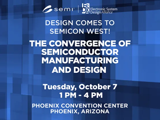
This year’s SEMICON West has new dates, a new location in a new city and a new addition to the program—design! “The Convergence of Semiconductor Manufacturing and Design” will highlight the collaboration between semiconductor manufacturers and chip design teams to bring advanced systems to market. The three-hour session during SEMICON West will be held Tuesday, October 7, from 1-4 p.m. at the Phoenix Convention Center in Phoenix, Arizona.Five 20-minute presentations will describe successful collaborations and address challenges and opportunities about design and manufacturing security, long-term reliability, system performance issues, and modeling and verification that encompass the entire system. Attendees can expect to learn about the key drivers behind the need for collaboration that range from heterogeneous integration to advanced packaging technologies and applications such as automotive and medical.Session moderators are Ming Zhang, PhD, Vice President of Fabless Solutions of PDF Solutions, and me. “As design and manufacturing complexity continues to grow, driven by applications like AI, it is becoming increasingly difficult to account for every manufacturing variation during design and at sign-off or to fully anticipate the entire design space at chip and system levels during manufacturing technology development,” said Zhang. “Achieving tighter integration between design and manufacturing through broader and deeper data and methodology collaboration will be critical to improving predictability, accelerating time to market and enabling the next generation of semiconductor innovation.”It’s within this context that we selected the presenters who include:“Revolutionizing Silicon to Systems Design: Unlocking the Future with 2.5D and 3D Multi-Die Innovations” by Sutirtha Kabir of Synopsys.“Manufacturing to Development to Manufacturing for Circular Collaboration Leveraging AI and Other EDA Advances” with David Kelf from Breker Verification Systems.“Bridging the Silicon Divide: Converging Chip Design and Manufacturing in the Era of High Integration” from Lu Dai at Qualcomm Technologies.“3D and Chiplets Driving Moore’s Law into the Future” with Joe Kwan of Siemens EDA.“Multiphysics Multiscale Challenges and Solutions for 3D Heterogenous Integration” by Sudarshan Mallu from Ansys, part of Synopsys.The program concludes with a panel moderated by Zhang titled “The Convergence of Semiconductor Manufacturing and Design” and features the session presenters.Join us to learn how the semiconductor manufacturing and design communities are collaborating to deliver advanced systems based on chiplets and rapidly emerging packaging technologies including 2.5D and 3D ICs and MCMs. Audience participation will be encouraged.Also of interest to attendees is a SEMICON West keynote from John Kibarian, CEO, President and Co-Founder of PDF Solutions who is also co-chair of SEMI’s ESD Alliance Governing Council. Kibarian will address “Revolutionizing Semiconductor Collaboration: The Emergence of AI-Driven Industry Platforms” during the CEO Summit keynotes on Wednesday, October 8 at 10:20 a.m.SEMICON West 2025 makes its debut in Phoenix, October 7-9 at the Phoenix Convention Center. This milestone event gathers global leaders across the microelectronics supply chain to explore transformative technologies, develop the future workforce and drive strategic collaboration. Moving SEMICON West to Phoenix highlights Arizona as a key hub for innovation and industry growth. Visit the SEMICON West homepage for more details on full program, including “The Convergence of Semiconductor Manufacturing and Design” session, special features, sponsors and exhibits. Registration is open. Robert (Bob) Smith is executive director of the ESD Alliance, a SEMI Technology Community. 
Read More
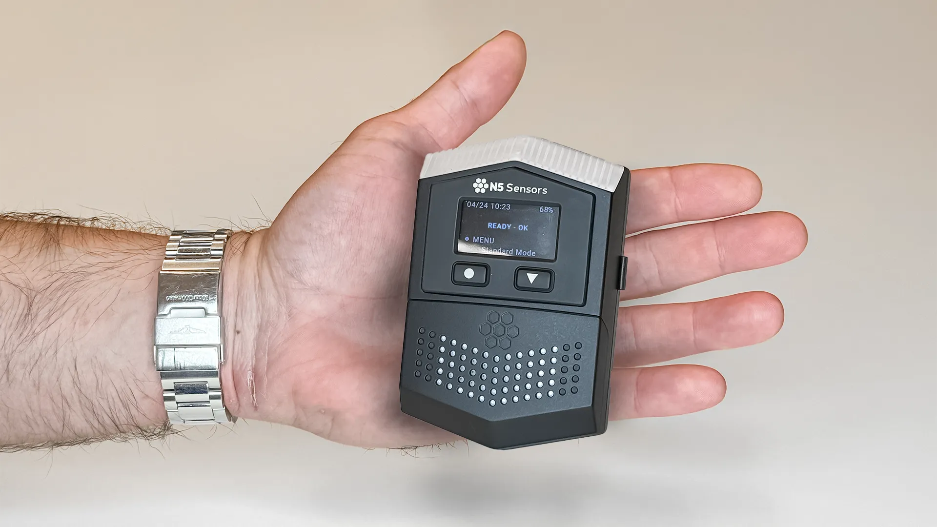
BackgroundSEMI’s Device Working Group, part of its MEMS Sensors Industry Group (MSIG), actively works to lower barriers for MEMS-based gas sensor market adoption. In 2022, the group published SEMI MS14 – Guide for Critical Parameters of Gas Sensors [1, 2], which recommends guidelines for gas sensor product datasheets to improve standardization and adoption.This article explores what gas sensors are, how they are calibrated, what their limitations are, and how the next generation of MEMS-based gas sensors is driving innovation. Here, we utilize terminology that the most common, accepted, and recognizable across different sensing communities.From Gas Sensing Elements to Gas Detector SystemsFigure 1 highlights the primary components related to gas sensing. The most fundamental component, the gas sensing element, responds to changes in gas concentration. It is an analog circuit without additional electronics, and it often has only one output like resistance, current, light intensity, or voltage. It is sometimes called a gas sensor, but the recommended terminology is gas sensing element. Such terminology is the most popular, accepted, and recognizable across different communities.Figure 1: Components related to a gas sensorThe gas sensing element can connect to an additional electronic circuit that includes a signal conditioning module, an analog-to-digital converter, and as of recently, an onboard edge data processor. MEMS microfabrication technology allows multiple gas sensing elements and electronic circuit components to be fabricated as an integrated circuit module. These elements can be as small as a grain of rice. This combination of elements is often called a gas sensor, gas sensor system, or gas sensor module. However, the recommended terminology is gas sensing module.The gas sensing module can connect to additional electronic components such as power management, communication, human-machine interfaces, and others. It can also be supplemented with software or firmware and packaged in a mechanical enclosure to create a complete gas sensing instrument. Such gas monitors can be designed as stand-alone, stationary, handheld, or wearable systems, or embedded into bigger systems. The gas sensing instrument is commonly referred to as a gas detector, gas monitor, or gas sensor node, but the recommended terminology is gas detector.Gas Sensor CalibrationGas sensor calibration involves exposing a gas sensing element, module, or detector to various gas concentration standards under application-specific conditions. The output is then adjusted to match these standards, and the sensor is calibrated when the output aligns with the tested gas concentrations.Calibration provides information on uncertainty, non-linearity, and other parameters such as tested gases and their concentrations, and interferents such as ambient humidity and temperature and other gases. CoGDEM Guide to Gas Detection [3] describes common calibration routines and the factors affecting calibration. Companies that serve industrial safety markets also describe the necessary equipment and calibration technologies and offer guidelines and tutorials [4-6].A gas detector should operate under the expected application conditions to ensure it reports gas concentrations accurately. Examples of such conditions may be indoors, urban outdoors, industrial outdoors, exhaled breath analysis, and others. Accuracy refers to how closely the sensor readings match the actual gas concentrations. A calibration plan should account for all quantitative effects of these conditions. Figure 2 illustrates various gas detector accuracy levels and presents both complete coverage (full factorial) and partial coverage (fractional factorial) calibration plans [7]. These plans help manage calibration costs and complexity.Figure 2: Examples of full factorial and fractional factorial calibrations and correlation plot of benchmark versus sensor responsesThe calibration parameters are saved on the gas detector to convert measured responses into gas concentrations. In addition to traditional algorithms for industrial safety gas sensors, multivariate machine learning algorithms are also emerging. These algorithms can incorporate responses from the gas sensing element, along with contextual inputs from auxiliary sensors for interfering gases, temperature, humidity, and pressure. This data can be available on-board of the gas sensing module, on-board of the gas detector, or through the cloud. The calibration cost significantly increases the total production cost of mass-produced gas detectors because it adds additional steps and is time- and cost-intensive, but new approaches based by advanced algorithms have emerged that reduce calibration time and lower calibration costs [8, 9]. Not all gas detectors report individual gas concentrations. Some gas sensing applications only detect when a gas level reaches a specific threshold, for example a residential carbon monoxide alarm. Other gas detectors provide multiple air quality index values by accurately measuring concentrations of five pollutants: ozone, carbon monoxide, nitrogen dioxide, sulfur dioxide, and particulate matter of 2.5 mm and 10 mm [10]. These detectors are typically used for urban outdoor applications. Limitations of Single Output Gas Sensing Elements Prevent Their Acceptance in Many New AreasAvailable amperometric electrochemical sensors, semiconducting metal-oxide chemical resistors, pellistors, thermal conductivity sensors, and many others utilize gas sensing principles that were developed between the 1930s and 1970s. These innovations marked a significant advancement over using canary birds to detect carbon monoxide or miner’s lamps to identify methane in coal mines and other harsh environments. Early sensors relied on strong signals from a sensing element that measured high concentrations of a gas. Over time, engineers miniaturized these sensing elements without changing their underlying design principles, and today, the same sensing methods are still widely used to detect relatively high concentrations of specific gases for safety applications. However, single output gas sensing elements cannot mathematically differentiate various gases that produce similar sensor signals. They also cannot identify different sources affecting the sensor signal. Further, as the measured gas concentrations are getting smaller, the response drift of the sensing element and effects from other gases in air become more pronounced, reducing detector accuracy.For this reason, the United States Environmental Protection Agency recently highlighted that existing gas detectors have inherent limitations crucial to understand before collecting and interpreting data [11]. A Nature Perspective also noted that ambient interferences could make the data from single-output gas sensors “essentially meaningless” [12].Next Generation MEMS Gas Sensors: Solutions for Accurate and Stable Calibrated Gas Sensing Gas sensor developers and manufacturers are creating solutions that maintain accurate gas sensor performance at lower target gas concentrations over extended periods of time for chemically complex environments without increasing the hardware size or the amount of power consumption [13-15]. These solutions, inspired by traditional gas chromatography, mass spectrometry, and laser spectroscopy detectors that have exceptional gas-recognition abilities that are enabled by one or several independent response variables, which are factors that are varied in the detector in a controlled fashion. Examples of independent response variables are retention time in gas chromatography, mass-to-charge ratio in mass spectrometry, and wavelengths in laser spectroscopy. Although these traditional detectors are relatively large and expensive, they deliver significant societal benefits in exquisite multi-gas detection in chemically complex environments that have earned three Nobel Prizes [16]. SEMI’s MSIG Device Working Group is exploring the tremendous opportunity to emulate the mathematical principles of these large and expensive traditional gas detectors for miniature gas sensors [17, 18]. Our approach is to move beyond the limitations of single-output gas sensing elements and to preserve accurate gas detection in diverse operational scenarios. Right now, scientists and engineers are designing the next generation of miniature gas detectors to operate one or more gas sensing elements under measurement conditions that suppress or eliminate ambient interferences, boost stability, and reduce power consumption. To enhance gas sensing accuracy and stability, metal oxide gas sensing elements are modulated by gas sensing modules using temperature modulation [19] (e.g., Bosch, Renesas, 3S Technologies), dielectric excitation [20] (e.g. GE Vernova) or photoactivation [21] (e.g. N5 Sensors). Miniature electrochemical sensors use bias modulation and incorporate multi-frequency impedance enhanced readouts [15], whereas acoustic resonant sensing elements are modulated by temperature and multi-frequency impedance enhanced readouts of multiple harmonics [22]. Additionally, stable multi-element, multi-pixel, and multi-modal gas sensing elements are combining different sensing principles to gather more information from the same event, delivering more accurate responses. Figure 3 conceptually shows how these next-generation gas sensors should be able to compete with the traditional large and expensive analytical instruments on performance without the burden of high SWaP-C (size, weight, power, and cost) [23].Figure 3: Next generation gas sensors competing with exquisite performance of traditional analytical instruments, but without their high SWAP-C burden. SWaP-C stands for size, weight, power, and cost.ConclusionThe next generation of gas detectors promises to deliver high performance in diverse and complex environments by overcoming the limitations of single-output gas sensing elements and integrating advanced algorithms and multi-modal sensing techniques. These innovations will not only enhance safety and quality of environmental monitoring, but they will also open new applications for various industries. As the gas sensing field continues to evolve, interdisciplinary collaborations and continued research will be critical for unlocking the full potential of these technologies.Radislav A. Potyrailo is a Sr. Principal Scientist at GE Vernova Advanced Research.Andreas Schütze is a Professor at Saarland University.Sreeni Rao is a VP of Product Management and GM of Environmental Sensing at Interlink Electronics.Christian Meyer is a Sr. Manager of Application Engineering at Renesas Electronics Corporation.Paul Carey is Director of MEMS Sensors Industry Group at SEMI.References1. SEMI MS14 - Guide for Critical Parameters of Gas Sensors. SEMI: 2022; https://store-us.semi.org/products/ms01400-semi-ms14-guide-for-critical-parameters-of-gas-sensors.2. Rao, S.; Potyrailo, R.; Sakauchi, R.; Carey, P., SEMI MS14-0422 Standard: Critical Parameters of Gas Sensors For Emerging Applications. SEMI Advanced Sensors Seminar Series: 2023; p https://semi.huihuidehui.workers.dev/sites/semi.org/files/2023-05/SEMI-Gas%20Std%20Webinar%20V14_230531.pdf.3. Greenham, L., The CoGDEM Guide to Gas Detection. ILM Publications: 2012.4. Gas Detector Calibration Procedures, Requirements and Tips, Industrial Scientific 2025, https://www.indsci.com/en/blog/gas-detector-calibration.5. Gas Detector Bump Test: Bump Testing and Calibration of your Gas Monitors, PK Safety 2025, https://pksafety.com/blogs/pk-safety-blog/bump-testing-and-calibration-of-your-gas-monitors.6. What Are Calibration and Bump Tests for Portable Gas Detectors: Key Differences and Ways to Help Streamline Compliance, MSA 2024, https://blog.msasafety.com/what-are-calibration-and-bump-tests-for-portable-gas-detectors/.7. Ryan, T. P., Modern Experimental Design. Wiley: Hoboken, NJ, 2007.8. Fonollosa, J.; Fernandez, L.; Gutiérrez-Gálvez, A.; Huerta, R.; Marco, S. Calibration transfer and drift counteraction in chemical sensor arrays using direct standardization, Sens. Actuators B 2016, 236, 1044-1053.9. Robin, Y.; Amann, J.; Schneider, T.; Schütze, A.; Bur, C. Comparison of Transfer Learning and Established Calibration Transfer Methods for Metal Oxide Semiconductor Gas Sensors, Atmosphere 2023, 14, (7), 1123.10. Technical Assistance Document for the Reporting of Daily Air Quality – the Air Quality Index (AQI), US Environmental Protection Agency 2014, EPA-454/B-24-002.11. Barkjohn, K. K.; Clements, A.; Mocka, C.; Barrette, C.; Bittner, A.; Champion, W.; Gantt, B.; Good, E.; Holder, A.; Hillis, B. Air Quality Sensor Experts Convene: Current Quality Assurance Considerations for Credible Data, ACS ES T Air 2024, 1, (10), 1203–1214.12. Austen, K. Pollution patrol, Nature 2015, 517, 136-138.13. Bur, C.; Bastuck, M.; Spetz, A. L.; Andersson, M.; Schütze, A. Selectivity enhancement of SiC-FET gas sensors by combining temperature and gate bias cycled operation using multivariate statistics, Sens. Actuators, B 2014, 193, 931-940.14. Schütze, A., Keynote: High performance gas measurement systems – bridging the gap between sensors and analytics. IEEE International Symposium on Olfaction and Electronic Nose (ISOEN), Grapevine, TX, May 12-15: 2024.15. Potyrailo, R. A. In Cross-Pollination of Electronics and Mathematics: Unlocking New Horizons in Ambient Gas Sensing, SEMI MEMS and Sensors Technical Congress (MSTC) 2025, Georgia Institute of Technology, Atlanta, GA, March 26-27, 2025.16. The Nobel Foundation 2025, https://www.nobelprize.org/prizes/lists/all-nobel-prizes/.17. Potyrailo, R. A.; St-Pierre, R.; Crowder, J.; Scherer, B.; Cheng, B.; Nayeri, M.; Shan, S.; Brewer, J.; Ruffalo, R. First-order individual gas sensors as next generation reliable analytical instruments, Appl. Spectrosc. 2023, 77, (8), 860–872.18. Potyrailo, R. A.; Shan, S.; Cheng, B. Individual Optical Multi-Gas Sensors as Next Generation Second-Order Unobtrusive and Continuous Operation Analytical Instruments, Microchim. Acta 2025, Special Issue in Memory of Otto S. Wolfbeis, DOI: https://doi.org/10.21203/rs.3.rs-6234291/v1.19. Schütze, A.; Sauerwald, T., Dynamic operation of semiconductor sensors. In Semiconductor Gas Sensors, Elsevier: 2020; pp 385-412.20. Potyrailo, R. A.; Go, S.; Sexton, D.; Li, X.; Alkadi, N.; Kolmakov, A.; Amm, B.; St-Pierre, R.; Scherer, B.; Nayeri, M.; Wu, G.; Collazo-Davila, C.; Forman, D.; Calvert, C.; Mack, C.; Mcconnell, P. Extraordinary performance of semiconducting metal oxide gas sensors using dielectric excitation, Nat. Electron. 2020, 3, 280–289.21. Deb, S.; Mondal, A.; Reddy, Y. A. K. Review on development of metal-oxide and 2-D material based gas sensors under light-activation, Current Opinion in Solid State and Materials Science 2024, 30, 101160.22. Potyrailo, R. A., Tutorial: Next generation of gas sensors: anticipated and unanticipated advantages over last-century sensor designs. IEEE SENSORS, Vienna, Austria, Oct 29 - Nov 01: 2023.23. What is SWaP-C?, NSTXL National Security Technology Accelerator 2022, EPA-454/B-24-002.

Read More
In Q2, the SEMI International Standards Program made progress on several emerging initiatives. Together, we reached a critical milestone for one of our data standards initiatives with Document 6938C recently passing Technical Committee review in mid-June 2025. Ballot 6938C, which provides guidance on how to identify manufacturing equipment data provided by the equipment supplier that can be used in equipment engineering or analysis applications, is slated to join SEMI E190 and E190.1 in providing industry-enabling data standardization.In addition, we began major revisions to SEMI Standards S2, S8, and S10. These standards govern environmental, health, and safety (EHS) considerations, equipment user fatigue and injury reduction, and equipment risk assessment and evaluation, respectively. In our recently concluded North America Standards Summer 2025 Meetings, the NA EHS Technical Committee Chapter approved a revision ballot to SEMI S10. The ballot (7169) proposed several major revisions to the SEMI S10 Safety Guideline on risk assessment which included changes to references to equipment to objects under consideration. Other changes also included the relocation of the assessment of the risk of harm to property other than the OUC to a Related Information section. Additional details are provided below.We’re eagerly preparing for this year’s SEMICON West event, taking place for the first time ever in Phoenix, Arizona. We are also pleased to announce the return of the SEMI Global Standards Summit taking place Tuesday afternoon, October 7 at SEMICON West. Our inaugural Summit was held last year at SEMICON Japan 2024 last December. The Summit aims to identify standards-critical areas and work towards an industry standardization strategy for the next 3- and 7-year time horizons. This year's Global Standards Summit will feature sessions on Supply Chain Traceability as well as Environmental Sustainability. Similarly, as cybersecurity considerations become more complex, SEMICON West will host a dedicated Cybersecurity Forum from October 7-9 to address today’s most pertinent challenges. More detailed program information will be available soon. Finally, we’re looking forward to our SEMI Standards + Award Ceremony Networking Event at SEMICON West. Following the International Standards Meeting and Standards Summit on Tuesday, October 7, join us for appetizers, drinks, and great conversation from 6-7:30 p.m. In the meantime, learn more about becoming a member of the SEMI International Standards Program.Balloting for Document 6938Document 6938C introduces a new potential standard – Guide for Equipment Edge Data Governance. Under development by the Equipment Edge Data Governance (EEDG) Task Force since 2021, Document 6938C was balloted in Cycle 3-2025 and approved during the Information Control Taiwan Technical Committee (TC) Chapter meeting held on June 12, 2025. It has since received approval by the International Standards Committee Audits and Reviews Subcommittee and is now undergoing final processing for publication by SEMI. As manufacturing equipment offers more accessible data than ever, poor communication, inconsistent expectations, and data security concerns continue to halt or slow factory integration efforts. If passed, this new standard will help organize the information that supports smart manufacturing efforts at the edge. In addition, the EEDG Guide will provide a comprehensive set of best practices to both users and suppliers to increase the value of existing equipment data. Update on Revisions to SEMI S2, S8, and S10 Safety GuidelinesOur 2025 Q1 Standards Watch newsletter announced a significant overhaul for SEMI Standards S2, S8, and S10.S2, SEMI’s standard for performance-based environmental, health, and safety (EHS) considerations for semiconductor manufacturing equipment, is undergoing discussions on redefining safety interlock systems. The S2 task force will issue an informal ballot to the general audience for feedback. The results then will be used to develop a formal letter ballot.First developed in 1995, SEMI Standard S8 works to reduce fatigue and injury by matching equipment to the user’s size, strength, and range of motion. Although this safety standard has been periodically updated since its inception, its last substantial revision was in 2018. The ballot to revise S8 ultimately failed the EH S TC Chapter review at this year’s Winter Meeting. With 214 comments and negatives to consider, the task force is revising the ballot and plans to reissue in Cycle 7 of August 2025.Finally, SEMI Standard S10 is moving through ballot 7169. This standard defines a consistent means of risk estimation that other SEMI Safety Guidelines can invoke. Ballot 7169 will separate facility and building risk assessment to a non-normative portion of the document, ensure EHS risks are separately calculated from commercial object risks, and clarify risk assessment of observed events from risk assessment of foreseen events. Ballot 7169 results were reviewed on June 5 during the North America Standards Summer meetings. The document was approved and is being processed for publication by SEMI.Cybersecurity Forum at SEMICON West 2025This year’s SEMICON West will feature a dedicated Cybersecurity Forum to address the semiconductor industry’s rapidly-changing cybersecurity landscape. The SEMI Cybersecurity Forum will gather industry experts to share knowledge and experience on the following topics. The goal is to develop actionable strategies and a deeper understanding of current and future cybersecurity risks. Cybersecurity in Legacy Semiconductor ToolsEmerging and Existing Cybersecurity Legislation and ComplianceCybersecurity in Maintenance and ManufacturingImpact of Cybersecurity Events on Semiconductor Manufacturing OperationsSupply Chain SecurityThreat Landscape in Semiconductor ManufacturingThe 2025 call for abstracts is now closed. Speakers will be announced in Q3.SEMI E187 Compliance Guidance White PaperThe SEMI Semiconductor Manufacturing Cybersecurity Consortium (SMCC), in collaboration with industry experts, is pleased to announce the release of the SEMI E187 Compliance Guidance Whitepaper. This comprehensive resource is designed to support semiconductor equipment suppliers and device manufacturers as they work to meet the requirements of the SEMI E187 0122 Standard - The Specification of Cybersecurity of Fab Equipment.Professionals involved in tool development, manufacturing, operations, and security will find the guidance particularly relevant and actionable. It provides guidance to address all twelve SEMI E187 requirements and focuses on new to fab equipment.Download the Whitepaper for freeSEMI Standards North America Summer MeetingsThis year’s SEMI Standards North America Summer Meetings were held from June 2-5 at SEMI’s headquarters in Milpitas, California. The meetings convened 11 committees and 40 task forces to discuss topics ranging from EHS to facilities, 3D packaging, MEMS, and more. In addition to the results of ballot 7169, technical changes to ballot 6601B, New Standard: Guide for Meeting IRDS Yield Table Recommendations for High Purity Polymer Materials and Components Used in Ultrapure Water, was also approved by the Liquid Chemicals North America TC Chapter, since the activity began in 2019. A Ratification Ballot will be issued in Cycle 7-2025 to verify the changes. In total, over 15 activities, ranging from Auxiliary Information, Reapprovals, and Line-Item ballots, also recently passed Procedural Review by the International Standards Committee (ISC) Audits Reviews Subcommittee and will be forwarded to Publications for final processing. The next SEMI International Standards Meeting will be held at SEMICON West from October 7-9 at the Phoenix Convention Center. Some technical committees and task forces may meet virtually outside of this meeting set, so be sure to check the SEMI Standards calendar of events for updates. Standards Introduced in Q2 2025New and revised standards released in Q2. April 2025 standards: https://store-us.semi.org/collections/standards/stdpbc-0425May 2025 standards: https://store-us.semi.org/collections/standards/stdpbc-0525June 2025 standards: https://store-us.semi.org/collections/standards/stdpbc-0625Get InvolvedSEMI Standards development activities take place throughout the year in all major manufacturing regions. To participate, join the SEMI International Standards Program.SEMI Standards are available through individual download purchases or online via SEMIViews. Sign up for a 30-day SEMIViews trial.For more information, please visit the Standards website and events page. For any questions regarding SEMI Standards activities, please contact your local SEMI Standards staff. Paul Trio is Director of Standards at SEMI.
Read More
Ann Wu is CEO of EDA startup Silimate, developer of a co-pilot (chat-based GenAI) for chip and IP designers to find and fix functional and power, performance and area (PPA) issues in their designs. Rick Carlson is Vice President of Sales at ESD Alliance member company Verific Design Automation, provider of front-end EDA platforms to a range of small and emerging EDA companies like Silimate and larger EDA vendors.I recently talked with Ann and Rick who represent EDA’s new and old guard. I found them to be bullish about the emerging EDA space called AI EDA that uses GenAI and large language models as the foundational tools and the swelling numbers of well-funded startups entering this space.Smith: Ann, you were an Apple hardware designer. What encouraged you to leap into entrepreneurship using AI as the foundational technology?Wu: It was always my goal. Apple afforded me the opportunity to understand how one of the best companies producing some of the most cutting-edge chips in the world operates. It also gave me the opportunity to work with some of the most brilliant engineers and operators. My plan was then to go back to Stanford to explore and start a compelling venture with another similarly motivated friend, Akash Levy. That was the genesis of Silimate. The drive for leaping into entrepreneurship then ultimately stemmed from my frustrations with the existing chip design process. I sensed there was an opportunity to apply AI technology to solve some of these limitations of the existing approaches to chip design.Smith: What made you think that AI would be applicable to the EDA challenges that designers face?Wu: AI provides a compelling solution to some of the intractable problems that have existed in EDA. Traditional EDA solutions solve isolated problems through heuristic algorithms. There’s a high volume of gray area between the well-defined boxes of inputs and outputs that had previously been unsolvable. Now with AI, there is finally a way to sift through and glean patterns, insights, and actions from these gray areas.That’s the macro reason why there's so much excitement and appetite around the application of AI for EDA.Smith: It sounds like productivity enhancement. What are some other key words or selling points to use to convince a designer of AI’s potential for EDA?Wu: I would say "speedup" is one of those keywords. Ultimately, the designer is trying to meet or even shorten the time to tape out while hitting their design spec. That's driving all decisions, whether to throw more headcount at closing a certain block or to defeature something that's going to cause the team to miss the shuttle. It all comes down to whether a fully featured and functional design gets to tape out and gets to market ahead of competitors.Productivity as a keyword is not compelling. It’s hard to translate how saving minutes or hours of an engineer's time connects back to the bottom line. The bottom-line decisions are driven by the project’s timeline as time to market is everything.What’s needed is a way to sift out and resolve real design problems 100x faster, which ultimately results in real speed up on a project’s schedule. For example, processing large amounts of data with AI to find issues actively helps the designer converge their design to their target.Finding and resolving issues in a design within minutes instead of days or weeks instead of months is the kind of impact that directors, VPs, and managers want for adopting new tools.Smith: What is driving hardware designers into this EDA space?Carlson: The thing that's most intriguing is large language models, neural networks and AI. It seems like an “aha” moment when startup founders believe they can do something that's dramatic for the first time.When I look back over my photobook of moments in my time in the EDA industry, there's the wonderment. The things that can be brought to bear with iterative versions of new technology from companies like Ann's will offer multiple “aha” moments. This is game changing.Smith: Are venture capitalists investing in EDA again?Carlson: Yes. Some venture capitalists haven't invested in EDA for decades. These are smart people. They have plenty of good people that can do good due diligence. The amount of money that's being invested is significant. It's not just a little bit of seed funding. One startup’s first round was $3 million. They're now raising $20 million in the next round. They're saying that their pre-money has to be $50-$60 million. They're just coming out and there's a huge amount of interest.We're going to be looking back in a year and say we just couldn't believe how much money is pouring into this. It has a huge impact on the world stage. This is an amazing time to be doing anything in and around the design of computer chips.Smith: Y Combinator (YC) invested in Silimate.Wu: Yes, that's right. It's an honor to be the first EDA company that YC had invested in. The semiconductor and EDA space had been under the radar until recently—it’s such a critical piece of our technical infrastructure. The semiconductor industry hasn't been headline news in past years. Now every other day, the Wall Street Journal runs some semiconductor chip-related article. People are realizing this is a fundamental piece of our world's tech stack, and the software that drives this tech stack is equally important and there are investments to be made.Learn more about Verific and Silimate during the 62nd Design Automation Conference (DAC).Verific will exhibit in Booth #1316 at the Moscone Center in San Francisco from June 23-25.Silimate’s Akash Levy, Founder and CTO, will participate in a panel titled “AI-Enabled EDA for Chip Design” at 10:30am on Tuesday, June 24, 2025.Robert (Bob) Smith is executive director of the ESD Alliance, a SEMI Technology Community.
Read More
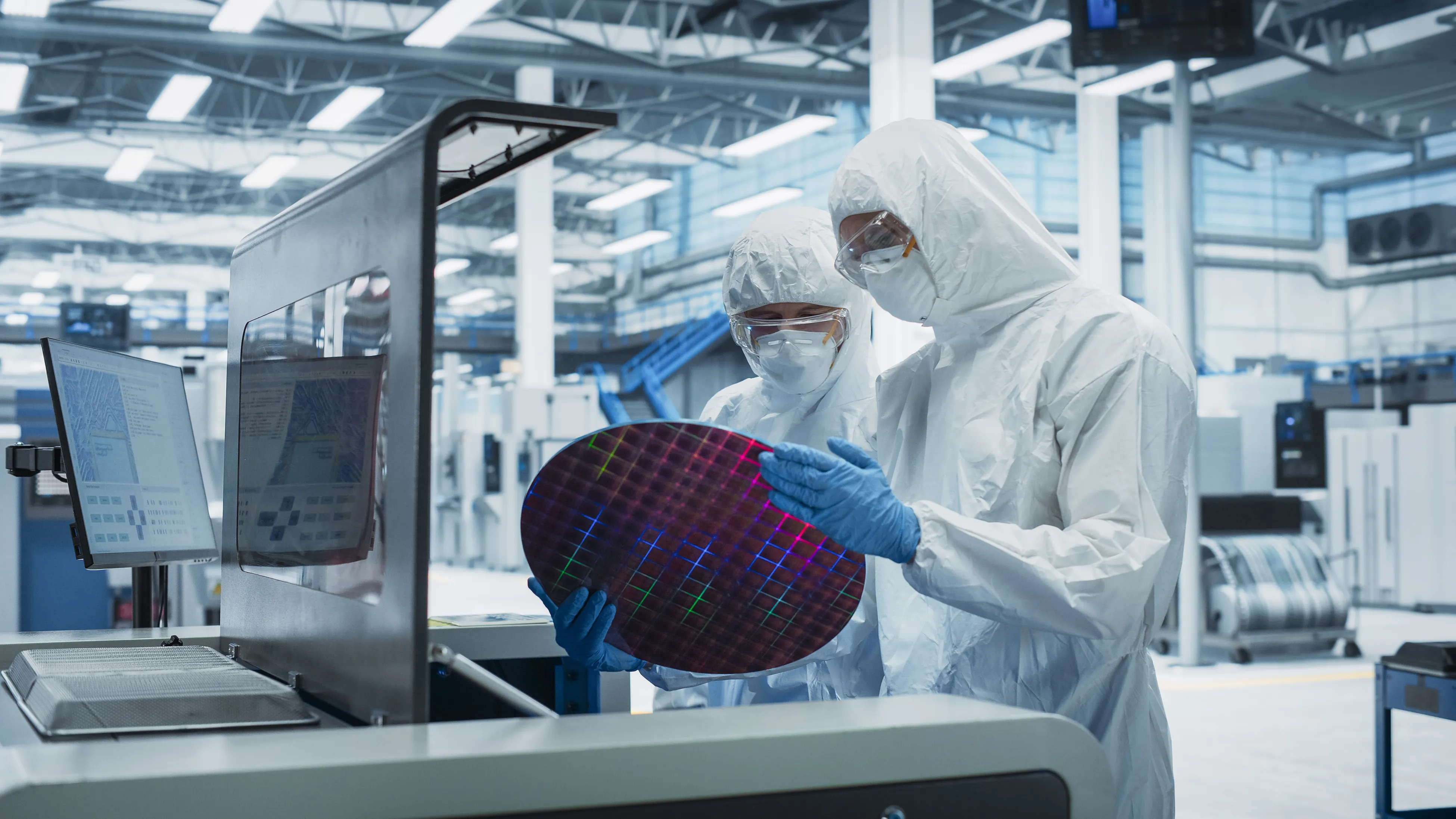
The semiconductor industry is on track to expand and launch 97 new high-volume fabs online worldwide from 2023 through 2025, a major milestone that highlights the massive investment in chip production capacity. This rapid expansion is expected to drive a sharp increase in the deployment of pendulum valves. These valves, found in tens of thousands of semiconductor tools, are critical to the wafer manufacturing process.  Though hidden inside complex etch and deposition chambers, pendulum valves play a vital role in semiconductor manufacturing. They regulate gas flow and maintain the vacuum conditions required for precise wafer processing, ensuring efficient etching or deposition by controlling gases, managing exhaust flows, and maintaining chamber integrity. But what happens if a pendulum valve fails? It disrupts the vacuum necessary for wafer processing, causing chamber contamination and potentially ruining wafers. This leads to costly material scrapping, unplanned downtime, and production delays. Persistent failures can damage the turbo molecular pump or the entire tool, significantly increasing repair costs. Clearly, pendulum valves are essential for the reliability and performance of semiconductor equipment, particularly in etching and deposition chambers. Here are four critical reasons why:Consistent Vacuum Control: Maintaining a consistent vacuum environment is crucial for uniform layer deposition and etching, directly impacting the yield and performance of semiconductor chips. These valves regulate pressure and gas flow to ensure consistent and precise wafer fabrication processes. Contamination Prevention: Contaminants are a semiconductor manufacturer’s worst nightmare. Even microscopic impurities can destroy a wafer. Pendulum valves mitigate this risk with high-quality sealing mechanisms that create airtight environments, leading to high quality wafers and reducing waste.  Enhanced Yield: Pendulum valves are vital to achieving the highest possible yield in wafer manufacturing. Their ability to maintain operational stability and enhance process efficiency leads to fewer defects and higher productivity. By precisely controlling gas flows and preventing contamination, these valves reduce the likelihood of wafer defects and improve overall throughput. Minimal Footprint: Semiconductor fabs are high-tech, high-density environments where every square inch counts. Pendulum valves are designed with compact dimensions, allowing engineers to maximize production capacity without compromising performance or reliability.  Seal Performance Defines Valves’ Longevity  One of the core components of pendulum valves is its seals, directly impacting its durability, reliability, and maintenance. High-performance seals minimize downtime, reduce maintenance costs, and ensure a long operating life. However, achieving this performance requires attention to the challenges in semiconductor processes that impact performance and lifespan. Exposure to aggressive chemicals and plasma environments can degrade seals, causing erosion, sticking, and cracking. Continuous dynamic motion, including compression, decompression, and rotational movements, leads to friction and wear, shortening seal longevity. Errors, such as improper installation of static seals, can disrupt valve operation and cause delays. Extreme heat in wafer fabrication further tests the durability of valve components, while poor maintenance increases the risk of failures, resulting in costly downtime and repairs.  To keep valves operating at their peak efficiency, manufacturers need to prioritize five types of seals, identifying potential risks and tackling them effectively. The Pendulum Plate Face Seal, a dynamic component, must endure repeated compression and decompression during use. This constant motion, coupled with exposure to harsh chemicals, makes the seal vulnerable to issues like sticking and cracking. Without proper installation and attention, extreme failures, such as the seal dislodging entirely, can occur, disrupting operations.  Similarly, the Pendulum Plate Radial Seal performs a vital role, moving vertically within a piston bore. This component faces threats such as rolling, twisting, and chemical degradation, often leading to cracks or even fragmenting under severe torsional stress.   The Bonnet Seal, though static, is not exempt from potential difficulties. Improper installation or material cracking can severely compromise its functionality.  For dynamic applications like the Rotating Paddle Shaft Seal, friction is a constant adversary, compounded by chemical exposure that accelerates wear and tear.  Lastly, the Actuating Pins Seal, pivotal for enabling precise up-and-down movement within a piston bore, is particularly sensitive to installation errors.  When Failure is Not an Option  Addressing these challenges is essential to maintain the reliability and longevity of pendulum valves in semiconductor manufacturing. Greene Tweed uses a structured framework ‘Right Seal Pyramid’ to select the most suitable seal for every application. This process considers key factors like material compatibility, seal geometry, and operating conditions to develop solutions tailored to the specific needs of semiconductor manufacturing. By aligning seal types with precise engineering criteria, the Right Seal Pyramid methodology addresses key challenges like chemical resistance, mechanical stress, and installation accuracy, ensuring reliable performance in the harshest semiconductor manufacturing environments.  Explore MoreWant to learn how to prevent premature pendulum failure? Catch our full webinar replay or download our Semiconductor Playbook for expert insights, innovative solutions, and best practices tailored to your most critical applications. Carmen Quartapella is a Senior Engineer of Design Analysis at Greene Tweed. Quartapella has developed deep technical expertise over a three-decade career that spans multiple facets of the semiconductor industry. Throughout his career, he has gained expertise in Semiconductor Engineering, Engineering Management, Sales, Business Management, and Emerging Technologies. He graduated from Drexel University with a degree in Mechanical Engineering
Read More