downloadGroupGroupnoun_press release_995423_000000 copyGroupnoun_Feed_96767_000000Group 19noun_pictures_1817522_000000Member company iconResource item iconStore item iconGroup 19Group 19noun_Photo_2085192_000000 Copynoun_presentation_2096081_000000Group 19Group Copy 7noun_webinar_692730_000000Path
Skip to main content
Default Banner Image

Technology and Trends

As artificial intelligence (AI) proliferates rapidly, AI models and datasets are also growing rapidly in size. This growth far outpaces performance improvement in hardware systems, and is increasing AI’s energy consumption unsustainably. To address these challenges and explore collaborative solutions, SEMI’s Smart Data-AI Initiative - as part of its Future of Computing focus - recently hosted a day-long workshop on Sustainable AI Systems that brought together domain experts from the entire AI ecosystem. Speakers included industry leaders Applied Materials, AMD, Arm, ASE, Google DeepMind, IBM, Intel, Lam Research, McKinsey, Micron, NVIDIA, Qualcomm, SK hynix; exciting start-ups Cerebras, LightMatter, Mentium Technologies and Mueon; and leading-edge academic institutions, Stanford University and University of California, Davis Irvine. The keynotes, panels and spirited audience discussions covered novel devices, materials, advanced packaging, chiplets, photonics and architectures algorithms for data centers, cloud edge. This article synthesizes high-level insights from the workshop.The AI ImperativeThe day started with a basic question – why is AI essential to continued progress and prosperity? The answer lies partly in shifting global demographics, with the population aging in most developed economies. At the turn of the century, there were ~6 people in the workforce supporting each retiree, but projections indicate there will be only 2 active workers per retiree by 2050. In parallel, productivity growth rates have fallen to half of what is required. AI can help bridge this gap, if we can ensure continued progress of AI in a responsible and sustainable manner.The Energy WallA formidable roadblock to continued progress of AI is its rising energy demands. For example, the energy used by some large language models (LLMs) to run just one training cycle could be used to power thousands of homes. The switch to transformer models has increased AI-driven computing demand by a factor of 50 million over 5 years, and by some projections, this demand will consume half the world's generation capacity by 2050. This is clearly not sustainable! All players in the ecosystem are deeply committed to reducing AI’s energy consumption, and the industry has already decreased the energy used per token of computing by a factor of 100K in the past 10 years. However, the rapid growth of AI outpaces this, highlighting the huge challenge ahead.The System StackThis workshop was developed with the hypothesis that innovation is required across all segments, and an important first step is to initiate a dialog. Our highly distinguished speakers covered the entire solution stack, and while it is impossible to capture the ocean of insights that they shared, the following provides a flavor.Materials DevicesMaterials and devices used to build semiconductor chips form the foundation of the stack for all computing systems. Silicon substrates with copper interconnects remain industry’s mainstay, but are being augmented by innovative ideas. As device dimensions continue to shrink, novel 2D materials such as MoSe2, WSe2, ZrSe2 and NbP are being researched. While Si mobility degrades with decreasing film thickness, 2D materials maintain high electron mobility in thin-film substrates. These can be stacked to build 3D systems with lower power consumption than traditional planar structures. In parallel, novel device technologies such as gate-all-around (GAA) can provide power savings up to 25%.These novel materials and devices are complex, and require almost magical wizardry to build. For example, they may require depositing a stack of multiple defect-free films that are only a single (or few) atomic layer(s) thick, or etching a steep well that is one hundred times as deep as it is wide. It is an incredible accomplishment of the semiconductor industry to build these devices and chips successfully, but it is getting harder and more expensive. Consequently, AI is now being used as a tool to help with this ever-growing fabrication complexity of semiconductor R D and manufacturing. This is a synergistic virtuous cycle, where AI algorithms enabled by chips are used in turn to help with chip fabrication.System IntegrationThe next layer of the stack is the integration of individual devices into a system. Advanced packaging techniques, such as silicon or glass interposers (2.5D) for interconnecting chips, can reduce the communication distance and power consumption. These are often deployed for high-performance computing systems running AI algorithms. Beyond this, the industry is actively exploring 3D systems that are even more compact, both as multi-die 3D packages and as monolithic 3D chips.The concept of chiplets – smaller chips with specialized functions that can be assembled flexibly to optimize system performance – holds much promise. Industry consortia are developing protocols such as Universal Chiplet Interconnect ExpressTM (UCIeTM) to enable seamless integration of chiplets both in the planar and vertical dimensions. These advanced techniques pack more functional elements into increasingly compact form factors, but this proximity makes power delivery challenging and often generates intense heat. Much work is needed to ensure optimal power delivery and adequate thermal dissipation.Looking beyond traditional electronics, photonics represents an exciting opportunity. Most long-distance data communication is on fiber-optic cables and thus already photonic – bringing this to shorter distances can save energy while increasing bandwidth and performance. This requires efficient photonic-electronic integration at the packaging or even chip level, which is a major challenge requiring cross-disciplinary collaboration.Architectures and AlgorithmsAI algorithms need enormous amounts of data processing compared to traditional computing workloads. This requirement stretches (or breaks) the limits of traditional Von Neumann architecture, which requires frequent data movement between memory and processor elements for each computation cycle. Much of current architecture innovation focuses on bringing processor and memory elements closer to each other. System integration is already driving “compute-near-memory” architectures like high bandwidth memory (HBM). Other forward-looking implementations combine them into a single chip, known as compute-in-memory (CIM). Memory elements being explored for this purpose include resistive RAM (RRAM), phase-change memory (PCM), ferroelectric RAM (FeRAM) and magnetic RAM (MRAM). However, there is no one “perfect” memory – each has pros and cons in terms of latency, capacity, bandwidth, power consumed per operation, manufacturability, etc. Other researchers are also exploring devices like memristors for analog computing, which can improve energy efficiency for certain workloads.Finally, hardware-software co-optimization is crucial. Algorithms mismatched with the underlying system are energy expensive; conversely, co-optimized systems are highly efficient. While conceptually obvious, this is difficult in practice because development cycles are quite different – software algorithms can transform in a few months, while new hardware often takes years to develop. While some strategies can be used for mitigation – such as designing in redundancy/flexibility or making the hardware application-specific – much work remains to solve this conundrum.Pre-competitive Collaboration to Find SolutionsAll speakers emphasized that pre-competitive collaboration across the entire stack is critical, as these challenges are formidable and cannot be solved by one entity or in isolated silos. SEMI is a global and neutral organization with over 3,000 member companies, and is well-positioned to provide a pre-competitive collaboration platform to connect the dots across silos. In fact, SEMI’s mantra is “Connect, Collaborate, Innovate” – reinforcing its commitment to advancing the entire industry. For this purpose, SEMI’s Smart Data-AI Initiative continues to drive robust discussions on this topic – next there will be a roundtable discussion during SEMICON Southeast Asia, May 20-22 in Singapore, followed by a focused technology session at SEMICON West 2025, October 7-9 in Phoenix, Arizona. The overall objective is to move from “talking-the-talk” to “walking-the-walk,” towards creating system-level solutions for energy-efficient AI computing. Specifically, we want to identify the pre-competitive actions that could synergize individual innovations and make the whole greater than the sum of parts. Some ideas include collaborative proof-of-concept projects, industry standards and independent benchmarking. Come join us on this journey and connect with us at [email protected]. Dr. Pushkar P. Apte is the Strategic Technology Advisor and leads the Smart Data-AI Initiative at SEMI.
Read More
As healthcare undergoes a digital transformation, semiconductor technologies are emerging as a critical foundational enabler, making care more personalized, proactive, and accessible. At SEMI, we’re proud to highlight the leadership of STMicroelectronics (ST), a member and active participant in our Smart MedTech initiative’s governing council, for their commitment to advancing this critical frontier.With decades of experience in sensing, power management, and connectivity, ST is helping to shape a future where electronic systems seamlessly integrate with healthcare and wellness solutions, empowering both patients and providers.The Rise of Wearables and the Role of SemiconductorsST has long delivered innovation in automotive, industrial, and consumer electronics. Now, the company is applying its expertise to wearable health technologies, a rapidly growing segment that’s reshaping how we monitor, diagnose, and manage health.Today’s wearables go far beyond their predecessors. They capture vital signs and biomarkers such as heart rate variability, ECG signals, blood pressure trends, and more with medical-grade accuracy, providing real-time insights that can inform treatment and improve outcomes. This evolution represents not just a technological leap, but a shift in how we deliver and think about healthcare.A Shared Mission to Scale MedTech InnovationST’s active engagement with SEMI’s Smart MedTech initiative reflects our shared commitment to building an agile, responsive ecosystem that can bring life-changing technologies to the market faster. Through Smart MedTech, SEMI unites leaders across the electronics and healthcare value chains to identify systemic barriers, spark cross-sector dialogue, and co-create strategies for scalable success.ST brings invaluable perspective and technical depth to this mission. Their approach focusing on full solutions rather than standalone components, demonstrates how semiconductor companies can play a central role in enabling integrated healthcare systems.Meeting the Moment: Prevention, Personalization, and ReachHealthcare systems globally face mounting challenges: aging populations, chronic disease burdens, rising costs, and a projected shortfall of 18 million healthcare workers (WHO, 2019). Against this backdrop, wearables and remote health monitoring tools are poised to deliver tremendous value.As ST points out, the economic case is clear: treating chronic disease can be 100 times more expensive than prevention, wearables offer a proactive path forward. By enabling continuous, at-home health tracking, these devices empower individuals to take control of their wellness and allow providers to intervene earlier and more effectively.Accelerating the Future TogetherAt the SEMI 2025 Technology Workshop, ST joined a panel discussion exploring how semiconductors are reshaping healthcare. The session highlighted the need for earlier diagnosis, personalized care, and scalable solutions amid rising chronic disease and healthcare labor shortages.Panelists emphasized moving beyond component sales to integrated, system-level solutions. ST’s role on the Smart MedTech governing council emphasizes their commitment to cross-sector collaboration and advancing MedTech adoption.The MedTech revolution requires more than great products, it demands aligned ecosystems, shared knowledge, and coordinated strategies. As a member of SEMI and a key voice in our Smart MedTech initiative, ST exemplifies how semiconductor innovation can drive real change in healthcare.We’re proud to work alongside ST and other industry leaders who are committed to creating smarter, more sustainable healthcare through electronics. Because in today’s healthcare landscape, an ounce of prevention enabled by semiconductors isn’t just worth a pound of cure, it’s a blueprint for global health resilience.See the full ST article STMicroelectronics and Medtech: Enabling Personalized Healthcare and Wellness through the Integration of Electronics featured on Smart MedTech webpage.Gity Samadi is Senior Director of R D at SEMI.Rafael Tudela Senior Technical Marketing Manager at SEMI.Michelle Smith-Moritz is Senior Program Manager, Smart MedTech at SEMI.
Read More
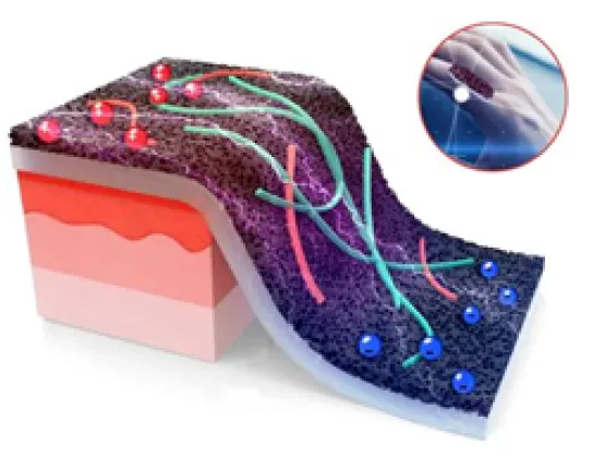
Say ‘Ahhhh’ – imagine your doctor monitoring a health condition from afar or emergency responders receiving real-time alerts that could save a life. A new smart sensor is taking the ouch out of wound monitoring. By using laser-induced graphene (LIG), a two-dimensional (2D) material, researchers are developing a sensor that could revolutionize the tracking of wound healing and recovery. Doctors could get a much clearer picture of the healing process, identifying issues like inflammation, physical strain or a spike in body temperature early on. "This unique sensor material we've developed has potentially important applications in health care monitoring,” said Huanyu “Larry” Cheng, James L. Henderson, Jr. Memorial Associate Professor of Engineering Science and Mechanics (ESM) at Penn State. LIG sensors are self-powered which means they could be especially useful for continuous monitoring in clinical settings or helping detect fires in remote locations. Source: Materials Research Institute, Penn StateUnder the Sea – Mechanical engineers at Carnegie Mellon’s Soft Machines Lab have created a soft robot inspired by the quick and agile brittle starfish, the first mobile and untethered underwater crawling robot. Named after Sponge Bob Square Pants’ sidekick, PATRICK is an AI powered robot which operates without motors so as not to disturb delicate sea life. To make the robot move, the researchers hit it with electric current, causing the wires to heat up past its transition temperature and allowing the limbs to contract and move in different directions. “We want to put the power and the electronics on-board with the robots,” said Ph.D. candidate and PATRICK creator, Zach Patterson. The soft robotic systems which are ideal for tracking the health and quality of water, are biodegradable to eliminate waste and protect the natural environment.Source: Carnegie Mellon University, School of Engineering The sky is NOT the limit with engineering – While Blue Origin made the news recently for sending an all women crew to the edge of space, the first Mexican born woman to travel into space is Katya Echazarreta, an electrical engineer originally from Guadalajara, Mexico. Echazarreta was selected for the trip from a pool of 7,000 applicants from more than 100 countries based on her outstanding achievements in the space industry, including five NASA missions. She traveled to space in 2022 aboard Blue Origin’s NS-21 flight as one of Space for Humanity’s citizen astronauts. Echazarreta comes from a family of engineers and works to make space exploration accessible to young kids, teens, women, and other scientists and engineers through Fundación Espacial, a foundation started in Mexico. Source: Astronomy.comMargaret Kindling is Senior Program Manager at the SEMI Foundation. She promotes inclusive workplaces via initiatives including Women in Semiconductors, Semiconductor PRIDE and workforce and career development programming at SEMICON West and SEMIEXPO Heartland.
Read More
With microelectronics manufacturing increasing in complexity and facing more cybersecurity threats, the SEMI International Standards Program has made crucial progress on efforts to address these challenges and others, in the first quarter of 2025. MEMS manufacturing readiness and cybersecurity came into sharp focus with the introduction of SEMI Standard MS15 - Guide to MEMS Manufacturing Readiness Levels. In addition, this quarter saw the opening of the public commentary period for a SEMI-led semiconductor manufacturing cybersecurity profile, developed for the National Institute of Standards and Technology’s (NIST) Cybersecurity Framework (CSF) 2.0. Through collaborative efforts, we held a successful North America Standards Winter Meeting in February, co-hosted a MEMS webinar, and published over 15 new and revised standards in areas such as equipment automation software, facilities, materials, and more.With exciting developments still to come, we’re looking forward to a wonderful year ahead.MEMS Manufacturing Readiness This March, SEMI unveiled its new standard, SEMI MS15 – Guide to MEMS Manufacturing Readiness Levels. This standard offers readiness level definitions, processes, and practices for creating MEMS products that meet targeted specification performance, quality, cost, and time-to-market. This standard is broken into eight distinct levels that cover basic research, all the way through high-volume production. Prior to the official release of SEMI MS15, we held a webinar that previewed how MEMS Manufacturing Readiness Levels will facilitate efficient MEMS development. Led by co-chair, Michelle Bourke of Lam Research, the SEMI MEMS Sensors Industry Group (MSIG) hosted a webinar featuring MEMS experts from SoftMEMS, HP, Teledyne MEMS, and Polar Semiconductor. Speakers shared insight into creating a structured and balanced MEMS manufacturing approach to drive successful products to commercialization. Cybersecurity Resilience Like 2024, cybersecurity remains pertinent in 2025. Last October, SEMI introduced SEMI Standard E191 and its subordinate standard, SEMI E191.1 to help define cybersecurity status information reporting. SEMI E191 and E191.1 join SEMI’s existing cybersecurity standards, SEMI E187 and E188. Last year also saw the development of the NIST CSF 2.0 Semiconductor Manufacturing Profile under SEMI’s Semiconductor Manufacturing Cybersecurity Consortium (SMCC). In partnership with NIST, SMCC advanced a community profile for CSF 2.0 that will serve as a cybersecurity framework specific to semiconductor manufacturing. The profile opened for public commentary between February 27 and May 30, with the final version slated for official release in Q3 of this year.As the semiconductor industry becomes increasingly reliant on digital technologies, we will continue to prioritize cybersecurity standards and initiatives essential for safeguarding the global supply chain.North America SEMI Standards Winter MeetingsFrom February 24 to 27 at SEMI’s headquarters, leaders from 11 committees and over 40 task forces collaborated on new and revised standards and safety guidelines for environmental, health, and safety, equipment automation and software, liquid chemicals, traceability, and more. Three SEMI Standard draft documents that were reviewed at the North America SEMI Standards Fall Meetings last November have also been approved and published. In addition to SEMI MS15, SEMI F122 – Guide for Facilities Data Package for Manufacturing Equipment Installation and Building Information Modeling, and SEMI E193 – Specification for 300 mm Film Frame FOUP (FFF), have also been approved and published. SEMI F122 suggests formats for reporting facilities data required to plan, prepare, model, and optimize a facility for the installation of manufacturing equipment by fab owners and manufacturing equipment customers. SEMI E193 drives consistent implementation of interfaces for film frame carriers that are compact and work with existing 300 mm FOUP standards and BOLTS interfaces. These standards are now available for purchase. The North America SEMI Standards Summer Meetings will take place from June 2-5 at SEMI’s Milpitas, California headquarters. Some technical committees and task forces may meet virtually outside of this meeting set – check the SEMI Standards calendar of events for updates!Standards Introduced in Q1 2025New and revised standards released in Q1. January 2025 standards: https://store-us.semi.org/collections/standards/lang-english+stdpbc-0125February 2025 standards: https://store-us.semi.org/collections/standards/lang-english+stdpbc-0225March 2025 standards: https://store-us.semi.org/collections/standards/lang-english+stdpbc-0325TestimonialsHear from Doug Suerich, Director of Marketing at PEER Group, how his work is helping shape smart manufacturing standards and global cybersecurity policies through our powerful collaborative platform. Get InvolvedSEMI Standards development activities take place throughout the year in all major manufacturing regions. To participate, join the SEMI International Standards Program.SEMI Standards are available through Individual Download purchases or online via SEMIViews. Sign up for a 30-day SEMIViews trial.For more information, please visit the Standards website and events page. For any questions regarding SEMI Standards activities, please contact your local SEMI Standards staff. Paul Trio is Director of Standards at SEMI.
Read More
In a world where technological advancements move at lightning speed, the semiconductor industry is facing unprecedented challenges. The demand for smaller, faster, and more energy-efficient devices is growing, and traditional manufacturing processes are being pushed to their limits. Enter Spin-on Dielectrics (SOD), a breakthrough material technology that offers a cost-effective, scalable solution for micro-gap filling and high-performance dielectric films. As the industry evolves, SOD is expected to play a pivotal role in enabling the next generation of chips that power everything from AI to everyday electronics.To learn more, SEMI Europe and Merck KGaA, Darmstadt, Germany, held a joint webinar that focused on semiconductor device process evolution by SOD. The session featured insights from three technology experts in the company, including Dr. Surésh Rajaraman, Executive Vice President and Head of Thin Film Business Unit, along with Atsuko Yamamoto, R D Manager for Spin-On Dielectric, and Go Nakano, Global Marketing Manager for Dielectric Materials.SEMI: What is SOD, and how does it fit within the broader semiconductor manufacturing process?Rajaraman: SOD, Spin on Dielectrics, is a unique class of materials used to deposit thin layers of dielectric films, which act as insulators or other functional films, on semiconductor devices. The fabrication of a semiconductor chip involves thousands of intricate steps that incorporate conductors, semiconductors, and insulators. SOD is a versatile technology that supports device performance and miniaturization by enabling better gap fill and film uniformity, all while offering attractive cost of ownership.SEMI: Why is there so much focus on SOD materials, and how are they evolving to meet future industry demands?Rajaraman: As semiconductor devices become more complex—such as 3D NAND scaling to more than 300 layers and DRAM incorporating pillar capacitors—there’s a growing need for materials that can address challenges like interconnect delays, power consumption, and heat generation while maintaining optimal performance. Traditional dielectric materials are reaching their limits, making Spin-on Dielectrics (SOD) a critical solution. SOD offers advantages like bottom-up and seam-free gap filling, enabling ultra-thin insulating and other functional layers that enhance electrical and thermal efficiency and support next-generation device scaling.The industry is pushing the boundaries of scaling, with increasing aspect ratios and complex structures in Logic, 3D NAND and DRAM. Modern devices now require deposition in features which are not only incredibly narrow but also increasingly deep due to going into the third dimension. This creates new challenges, such as stress buildup and cracking in conventional SOD materials. To overcome this, we are developing enhanced formulations with improved mechanical stability and polymer backbone engineering. These innovations enhance gap-filling properties and resistance to process-induced stress, ensuring SOD remains a key enabler for advanced semiconductor manufacturing.SEMI: What are the current industry trends driving the adoption of SOD?Nakano: SOD is becoming a key technology because of its excellent gap-filling performance. Unlike gas-phase deposition methods like Chemical Vapor Deposition (CVD) and Atomic Layer Deposition (ALD), SOD is a liquid-phase process. This makes it more efficient for high-aspect-ratio structures. It also helps reduce costs while maintaining high-performance dielectric properties.With increasing demand for high-density memory and logic devices, SOD is crucial for applications like DRAM and NAND flash, which require precise dielectric layer formation. In DRAM, we’re witnessing a shift from planar to vertical transistors, and even to monolithic 3D DRAM. These changes require new materials for gate insulators and electrodes, alongside improvements in aspect ratio gap filling.For NAND memory, manufacturers are increasing the number of memory layers, leading to taller memory stacks and deeper trenches. As lateral scaling progresses, narrower and more complex structures demand high-aspect-ratio trench fills to maintain performance and reliability.Logic devices are also evolving, with transistor structures moving from FinFETs to nanosheets and forksheets. This transition enhances performance, but it also introduces challenges in wiring density and electrical properties. The narrower pitch of wiring requires advanced dielectric solutions, like SOD, to enable reliable, high-performance semiconductor architectures.SEMI: With all these recent innovations, what role does Merck KGaA, Darmstadt, Germany play in supporting these advancements, and what does the company offer its customers? Rajaraman: As the semiconductor industry pushes the boundaries of scaling, doing so requires materials that can support increasingly complex structures. We are the only materials company in the industry to possess the full spectrum of process technologies for gap-filling capabilities, including SOD, ALD, CVD, and Flowable CVD. Our strategic acquisition of Versum Materials has expanded our capabilities with organosilicon precursors. Combined with our SOD expertise, it allows us to reengineer material backbones with more material choices and tailored properties to optimize performance in high-aspect-ratio applications.To support this, we’ve expanded our global R D footprint. We now operate in various application labs, enabling close collaboration with customers for material customization and fine-tuning properties to address specific manufacturing challenges. Last year, we inaugurated a new R D center in Korea as part of our commitment to being near our customers and accelerating time-to-market for next-generation semiconductor solutions. As semiconductor roadmaps become more complex, customization and collaboration also become more critical. The key to innovation lies in working closely with our customers, understanding their challenges, refining materials, and optimizing processes together. By fostering this ongoing partnership, we can accelerate technological advancements and ensure that new solutions align seamlessly with evolving industry demands.SEMI: Can you share some technical insights on SOD?Yamamoto: SOD is a key material used in semiconductor manufacturing to create insulating layers with high precision. One of the essential components in SOD is PHPS (Perhydropolysilazane), a polymer composed of silicon, nitrogen, and hydrogen. This material is applied as a liquid solution and transforms into a high-quality silicon oxide film through a series of thermal processes.PHPS is essential because it enables precise gap filling in extremely small structures, helping to improve device reliability. The process involves spin-coating the polymer onto a wafer, followed by pre-baking to remove solvents. Then, it undergoes high temperature curing in an oxygen and steam atmosphere, forming a dense silicon oxide film. This method ensures uniform coverage and cost efficiency compared to traditional dry film deposition techniques.Our Spinfil® product line has evolved over the past two decades, starting with the Spinfil® 400 series and advancing through the Spinfil® 600 to the widely used Spinfil® 800 series. These improvements have enhanced gap-filling capabilities and film uniformity, making them ideal for high-aspect-ratio trench structures. The critical baking process involves spin coating and pre-baking before wafers undergo batch processing in a high-temperature furnace. Controlled temperature and moisture conditions transform Spinfil® into silicon oxide films, optimizing properties such as refractive index, shrinkage, and etching resistance and ensuring reliability in semiconductor applications.SEMI: What are the latest trends in new polymer development for SOD?Yamamoto: Our research focuses on three key areas: enhancing film quality, developing SOD for high-aspect-ratio trench filling, and advancing low-k SOD for semiconductor processes.To improve film quality, we introduced the Neofil®series, an evolution of the Spinfil® 800 series. This innovation reduces film shrinkage, lowers stress, and enhances wet etching rates, making it ideal for next-generation semiconductor nodes.Our latest Neofil® series for high-aspect-ratio trench filling is targeted for traditional dry processes like CVD and ALD, which can often lead to void formation and require multiple deposition-etch steps. Our latest SOD materials address this by improving polymer elasticity, ensuring uniform filling of deep trenches up to 16 microns without cracks, making them suitable for emerging 3D nanostaircase designs.In low-k SOD development, we’re focusing on siloxane-based polymers, which provide excellent trench-filling capabilities while maintaining strong mechanical and electrical properties. Compared to flowable CVD and ALD, SOD offers a more cost-effective and efficient alternative. With continued advancements, we anticipate SOD will become a key material for future semi-damascene processes, enhancing embedding performance and overall device reliability.SEMI ContactSitong He, Communications Manager Email: [email protected]
Read More
The world is abuzz with the new opportunities being created by artificial intelligence (AI), enabled by availability of unprecedented amounts of data. AI runs on the semiconductor engine, and in turn, creates a rising demand for semiconductor chips. The semiconductor industry is predicted to reach $1 trillion in revenue by 2030 by McKinsey Co., in large part due to the market demand for AI and data. There are, however, formidable challenges to overcome for this virtuous cycle to continue. The SEMI Smart Data-AI Initiative, together with the SEMI Future of Computing Think Tank, is working to help the industry address these challenges. This article paints the big picture and lays the groundwork for an in-person workshop on March 19, 2025, in Silicon Valley, where pre-competitive and collaborative solutions will be explored.“To unlock the full potential of AI, innovation is required across the technology stack – from the models and software to datacenter architecture, chip design and how those chips are made. Advancements in foundational semiconductor technologies will have a dramatic impact on system-level energy and cost reduction in the AI datacenter.” – Gary Dickerson, President and CEO of Applied MaterialsThe Performance ChallengeInvestment in AI system infrastructure is rising at a dizzying pace, with hundreds of billions of dollars being committed by individual companies as well as public-private partnerships around the world. AI models built on larger data sets generally deliver better results, so model sizes are growing exponentially each year, with leading-edge models requiring billions and even trillions of parameters. This is especially true with the rapid growth of the Large Language Models (LLMs) used for Generative AI. Can the foundational semiconductor technology keep up? Even if semiconductor chips were following the famous Moore’s Law, performance would only double every 2 years. The real pace of performance improvement is even slower, as leading-edge technologies are reaching physical limits of materials – with the tiniest patterned dimensions on chips now approaching the fundamental atomic separation distance. While semiconductor designers and process technologists continue to innovate with new materials, devices, 3-dimensional stacking and so forth, there remains a formidable challenge for silicon chips and hardware systems to keep up with the growth rate of AI models and data sets. The Energy ChallengeProcessing ever-larger data sets and AI models also requires increasing energy. A recent report by the US Department of Energy indicates that data center energy consumption tripled over the past decade and may triple again in just 5 years! Other analyses show that a single data center powered by 20,000 GPUs can consume almost 40,000 KW, which is enough to power 31,000 homes in the US! Consequently, it is challenging for data centers to meet their power needs through public utilities, and several hyper scalers are investing in nuclear power. This acceleration in AI energy demand is further exacerbated because silicon technology evolution no longer follows power scaling with “Dennard’s Law,” which states that power density remains constant as technology scales to tinier dimensions. In fact, energy consumption of silicon devices has been increasing with technology scaling for the last decade. These combined factors give rise to the second formidable challenge – energy consumption is rising unsustainably for AI systems.Exploring SolutionsAddressing these challenges requires innovation from algorithms and architecture to foundational silicon technologies. The following are illustrative examples (not comprehensive) spanning the entire AI system stack.At the software and algorithm level, innovators are finding ways to reduce model size and to use hardware more efficiently. For example, IBM’s Granite models are smaller in size, with less than a billion parameters. Similarly, Google's Gemma platform offers small language models (SLMs). The recent market disruption from the publication of the DeepSeek reasoning model suggests that relatively smaller domain-specific reasoning models may offer significant efficiencies. At the architectural level, multiple paths are being explored. Special-purpose (or domain-specific) processing elements can deliver improved performance at equal or lower power for specific tasks. Examples include Cerebras’ wafer-scale designs with optimized AI accelerators and Mueon’s system-scale integration solutions. Another innovation path focuses on bringing computing closer to the memory elements, where the data resides. This addresses the major bottleneck between processors and memory in the traditional Von Neumann architecture, which has been the mainstay of the industry since inception. In-memory or near-memory computing, such as memory-focused architectures from Micron or processor-in-memory (PIM) solutions from SK hynix, offer higher performance with lower energy consumption for certain workloads. In parallel, leading CPU and GPU makers like AMD, Intel, and NVIDIA continue to innovate with power-efficient solutions. And “Edge Intelligence” innovations – for example, internet-of-things (IoT) solutions from Arm and Qualcomm – help reduce the processing and power load on data centers by executing more operations on edge devices.Critical enabling technologies also contribute significantly. Advanced packaging, for example ASE’s heterogeneous integration solutions, enable efficient, high-performance computing by integrating multiple diverse components optimally. Another emerging development is the advent of “chiplets,” which split the chip into smaller parts, and enable special-purpose accelerator building blocks to be assembled with more general processor, memory, and interconnect elements. A well-developed chiplet ecosystem could provide silicon designers with more degrees of freedom to design optimized systems. Looking beyond electronics, the integration of photonics can enable low-power, high-bandwidth connectivity – for example, LightMatter’s silicon photonics interconnects and Ciena’s data center interconnects.Materials and devices form the foundation of the technology stack. Example technology innovations include Stanford University-led N3XT, a 3D solution that integrates multiple novel devices and materials including resistive and spin-torque transfer RAMs, carbon nanotubes and 2D materials. Similarly, a University of California-led effort synthesizes low-dimensional nanostructures, sensors, detectors and photonics in an integrated solution. Finally, advanced and innovative processes and equipment are being developed – for example, by Applied Materials and Lam Research – to fabricate these novel materials and devices.All these individual innovations are amazing and necessary, but are they sufficient? What if we could collaborate across the entire system and co-optimize hardware and software innovations synergistically? Could the integrated whole be greater than the sum of parts? What efficiencies could we unleash? And what business opportunities would this unlock?The SEMI Future of Computing workshop on March 19, 2025, seeks to answer these questions by uniting AI innovation leaders from industry, academia and start-ups, including most of the companies and universities mentioned in this article. We will begin building pre-competitive collaboration that breaks through silos and explores system-level solutions – with the ultimate objective of radically improving the energy-efficiency of computing for AI.Pushkar Apte is the Strategic Technology Advisor and leads the Smart Data-AI Initiative at SEMI.Jim Sexton is a Fellow at IBM.Melissa Grupen-Shemansky is CTO and VP of Technology Communities at SEMI.
Read More
Superconducting Naturally – Miassite is a naturally occurring mineral which scientists at Ames National Laboratory have identified as the first unconventional superconductor found in nature. Unlike conventional superconductors that follow the Bardeen-Cooper-Schrieffer (BCS) theory, minerals such as miassite exhibit unique properties outside of this framework. Made of rhodium and sulfur, miassite was initially recognized as a regular superconductor in 2010. Recent tests confirm it joins a small, exclusive group of unconventional superconductors previously limited to lab-made materials.Lab tests on miassite involved measuring magnetic reactions, inducing defects, and analyzing energy gaps, all confirming its unconventional behavior. While naturally occurring, samples are unlikely to be superconductive due to their disordered state, miassite’s lab-verified properties open doors to new research and highlight its unique duality as both a conventional and unconventional superconductor.Source: A Superconductor Found in Nature Has Rocked the Scientific WorldPheromones + vision = mate selection – When choosing a mate, Heliconius butterflies, despite their tiny brains can outperform current AI in multi-sensory decision-making by processing visual and chemical cues simultaneously. This discovery inspired Penn State researchers to develop a low-energy, multi-sensory AI platform using 2D materials. The device combines molybdenum sulfide (MoS2) to mimic visual capabilities and graphene to detect chemical signals like pheromones.The device could integrate visual and chemical cues, offering adaptability like a butterfly’s mating behavior. This innovation addresses limitations in current AI, which relies heavily on energy-intensive, single-sensory processes. Researchers aim to expand the device to process three senses, like crayfish using visual, tactile, and chemical cues. The work, supported by the U.S. Army Research Office and the U.S. National Science Foundation, could revolutionize applications in robotics, smart sensors, and critical environments, by enabling AI systems to detect issues using multiple sensory inputs efficiently. Imaging of Heliconius Butterfly A Butterfly Effect – Proving once again that there is a lot to be learned from nature, researchers from the Fraunhofer Institute for Solar Energy Systems ISE have developed innovative, colored solar facade elements inspired by morpho butterfly mimicry. These panels are aesthetically pleasing, integrate seamlessly into building exteriors, and retain high efficiency, achieving 95% of the power output of uncoated panels. Using vacuum-applied 3D photonic structures like those on butterfly wings, the panels produce vibrant, angularly stable colors with minimal energy loss. This MorphoColor® technology addresses architects’ and building owners’ concerns about design, offering an efficient, visually appealing solution for building-integrated photovoltaics while surpassing other technologies currently available.Close up of a morpho butterfly wingSustainable Flight – The world’s fastest supercomputer, Frontier, located at Oak Ridge National Laboratory, enables unprecedented advancements in sustainable aviation technology. Capable of over a quintillion calculations per second, Frontier allows GE Aerospace to conduct full-scale simulations of its revolutionary Open Fan engine design, accelerating insights into aerodynamics and turbulence. This groundbreaking tool aids the CFM RISE program, which aims to cut fuel consumption and CO2 emissions by at least 20%. Frontier’s detailed simulations predict engine performance under real-world conditions, saving years of testing. The partnership between GE Aerospace and Oak Ridge is expanding, promising future collaborations in climate modeling and advanced simulation techniques.An Open Fan engine design developed as part of a new project led by GE AerospaceSource: https://www.geaerospace.com/news/articles/new-frontier-how-ge-aerospace-using-worlds-fastest-supercomputer-help-design-open-fanMargaret Kindling is Senior Program Manager at the SEMI Foundation. She promotes inclusive workplaces via initiatives like Women in Semiconductors, Semiconductor PRIDE and workforce development programming at SEMICON West and SEMIEXPO Heartland.
Read More
The sensor revolution is shaping the future of connectivity, with innovation in MEMS and imaging technologies paving the way for a smarter and more integrated world.As the world becomes increasingly interconnected, MEMS and imaging sensor technologies are driving transformative changes across industries, shaping the future of connectivity, intelligence, and sustainability. Powered by advances in miniaturization, AI integration, and sustainable design, MEMS and imaging technologies are enabling groundbreaking applications—from autonomous vehicles to wearable health devices—while addressing urgent global challenges like climate change and energy efficiency. At the MEMS Imaging Sensors Summit 2024, Laith Altimime, President of SEMI Europe, emphasized the pivotal role of MEMS and imaging technologies. Setting the stage for discussions on technological breakthroughs and market trends, Altimime remarked, “Sensors are at the heart of the next wave of innovation, enabling unprecedented levels of intelligence that are transforming industries and fostering a smarter, more sustainable, and seamlessly connected future.”Laith Altimime, President, SEMI EuropeStefan Finkbeiner, CEO of Bosch Sensortec, underscored in his opening keynote how advanced sensor technologies are enabling life-changing use cases. “Sensors are all around us, though we don’t always notice them,” emphasizing sensors’ ubiquitous role in smartphones, wearables, and hearables. Finkbeiner highlighted miniaturization as a key challenge, noting that even as sensors continue to shrink, they are increasingly integrated with edge AI to enable efficient, local decision-making.Stefan Finkbeiner, CEO, Bosch SensortecSimone Ferri, APMS Group Vice-President and MEMS Sub-Group General Manager at STMicroelectronics, highlighted the pivotal role of sensors as a bridge between the physical and digital world, noting “the most sophisticated machine is the human – so it is best to emulate human capabilities to enable the next generation of devices to accurately measure the parameters of your body.” Ferri stressed the importance of sustainability, advocating for smart, transformative, and precise sensors that provide meaningful data with optimal efficiency. By aligning technological innovation with environmental responsibility, Simone Ferri demonstrated how sensorization can enhance lives while enabling a net-zero transition across industries.Simone Ferri, APMS Group Vice-President and MEMS Sub-Group General Manager, STMicroelectronicsMEMS Growth Fueled by Piezo Materials and ElectrificationJean-Christophe Eloy, CEO and President of Yole Group, grounded the discussion in market data, forecasting a 5% CAGR for the MEMS market, which is set to exceed $20 billion by 2029. He highlighted key trends such as the increasing sophistication of automotive sensors—more cameras, higher resolution—and the impact of electrification. On the technology front, Eloy noted a “strong shift towards piezoelectric (piezo) MEMS,” driven by advancement in new materials like Lead Zirconate Titanate (PZT), Aluminum Nitride (AIN), and Scandium-doped Aluminum Nitride (ScAIN).Jean-Christophe Eloy, CEO and President, Yole GroupAlissa Fitzgerald, CEO of A.M. Fitzgerald Associates explored the expanding roles of MEMS technology in new domains, such as fiber optics for data centers. “Photonics is in the news,” she remarked, highlighting its potential to deliver 40% power savings compared to copper technologies. “MEMS manufacturing is set to evolve by 2030 and beyond,” said Fitzgerald, emphasizing the continued innovation in traditional wafer-based processes through the adoption of advanced thin-film materials like piezoelectrics and GaN. Furthermore, Fitzgerald discussed emerging manufacturing techniques such as 3D-printed MEMS and biodegradable materials to enable low-cost, sustainable sensors.Alissa Fitzgerald, CEO of A.M. Fitzgerald AssociatesAdding to the conversation on manufacturing, Jessica Gomez, CEO of Rogue Valley Microdevices, shared her perspective on how 300mm-capable MEMS foundries could “change the game,” improving production efficiency and lowering costs. Gomez also outlined the unique challenges of MEMS manufacturing, including the need for custom processes and the high-mix, low-volume nature of production.Advancing Smart Mobility Through Interoperable NetworksSmart mobility gained significant traction as Patrice Ancel, In-Vehicle Technologies Leader at BMW, tackled the intricacies of in-vehicle networking. Ancel shed light on the complexities of today’s vehicles, which contain 20,000 components and over 100 electronic control units (ECUs) from multiple suppliers. His message was clear: “Interoperability is key for us; without interoperability, none of this will happen.” Ancel’s call for collaboration resonated throughout the summit, highlighting the critical role of teamwork in driving innovation and progress within the automotive industry.Patrice Ancel, In-Vehicle Technologies Leader, BMWA Vision for the Future: Sustainability, Collaboration, and InnovationThe MEMS Imaging Sensors Summit demonstrated how collaboration, sustainability, and innovation are driving the sensor industry forward. From addressing market trends to tackling manufacturing challenges, the discussions revealed a shared commitment to creating a smarter, more connected world.On behalf of SEMI, the SEMI Europe team would like to thank the industry leaders whose expertise and enthusiasm made this summit a resounding success. SEMI ContactAna Bernardo, Manager of Technology ProgramsEmail: [email protected] Mobile: +49 175 4129 764Sitong He, Communications Manager Email: [email protected]: +49 151 5546 2638
Read More
Integrated photonics offers the semiconductor industry a new way to increase the speed and capability of classical compute functions, as well as enabling quantum computing. The III-V Summit, hosted by SEMI Europe in partnership with Photon Delta at SEMICON Europa, opened with a compelling question: why is a photonics summit taking place in the middle of a semiconductor event? Ajit Manocha, President and CEO of SEMI, highlighted the growing convergence of the semiconductor and photonics industries, stating, “It is my firm belief that a boost to Moore’s Law will come from the III-V world.” Declaring that the rate of growth in integrated photonics is set to pick up substantially, Manocha assured, “I will be your ambassador to make sure that the III-V technologies gain far greater visibility than they have today.”Ajit Manocha, President and CEO, SEMIThe promise of new III-V technologies is generating significant excitement within the semiconductor industry. Abdul Rahim, Ecosystem Manager at PhotonWorld, acknowledged the reality that today’s III-V device industry operates in a limited sphere, stating, “The III-V world is still at the interface of industry and academia. There is one main application for III-V devices – transceivers for data centers.” Abdul Rahim, Ecosystem Manager, PhotonWorld Carlos Lee, Director General of the European Photonics Industry Consortium (EPIC), echoed this message, “Photonics is not so much an industry today; it’s an ecosystem. It lacks the standards, roadmaps, and market data that a full-fledged industry needs – but we are getting there.” Carlos Lee, Director General, European Photonics Industry Consortium (EPIC)However, Rahim pointed to a number of trends that are driving the growth of III-V technology for integrated photonics. One key development is large-scale integration, “over the years, the number of devices in one photonics integrated chip (PIC) has been growing fast, reaching tens of thousands of components on-chip,” Rahim explained. Additionally, the widening frequency range supported by III-V devices is unlocking new applications beyond the telecom sector. Broad Scope of Research into III-V Technology for Integrated PhotonicsResearch into III-V technology spans an impressive range of materials, processes and applications. Nick Singh, CTO at Compound Semiconductor Applications (CSA) Catapult, a government-backed technology incubator, described in detail the most important fields of research that are driving innovation in integrated photonics. “III-V materials are special because they can be engineered,” Singh explained. Highlighting their potential role in advancing quantum computing, Singh added, “The ability to use new materials is crucial to reducing the reliance on algorithmic compensation for errors and non-linearity in hardware.” Nick Singh, CTO, Compound Semiconductor Applications Catapult However, Singh emphasized the need for the photonics industry to address structural challenges that could hinder progress. “Collaboration is crucial to standardize process development kits (PDKs) for photonics device fabrication processes—it’s like the Wild West in PDKs right now,” Singh remarked. “Additionally, the availability of raw materials presents a significant challenge.”The truth of this warning was confirmed by Diane Scott, Vice President of TECHCET, stating, "The US has deemed gallium to be the number one supply chain risk among a list of 50 raw materials, and the European Union (EU) has identified gallium as a critical raw material."Diane Scott, Vice President, TECHCETSuch geopolitical concerns have done little to dampen the intensity of research in III-V technology. One of the powerhouses of integrated photonics research is IBM, and Heike Riel, a Fellow at IBM Research with a special interest in quantum computing, revealed promising avenues that IBM is exploring. “IBM has developed local III-V-on-silicon heteroepitaxy, “Riel explained. “Using a direct growth method, we can grow vertical, lateral, and even 3D structures in III-V, such as stacked GaAs structures.” Riel highlighted the potential applications of this technology in emerging processor designs, including the Artificial Intelligence Unit (AIU) and analog computing devices with in-memory logic. “Here, we can deploy GaAs as a photorefractive material, used as a grating, to perform the same function as conventional electronic non-volatile memory in an analog computer chip,” Riel noted. Heike Riel, IBM Fellow, IBM ResearchAlso at the forefront of photonics integration is Black Semiconductor, a start-up company based in Aachen, Germany, which is developing devices using graphene. Cedric Huyghebaert, CTO of Black Semiconductor, shared the company’s vision, “We want to use electronics to compute, and photonics to transfer data, and bring both functions together on the same chip.” Black Semiconductor’s mission is to become the first foundry to offer integrated graphene technology. “Our ambition is to integrate graphene in line with semiconductor standards using semiconductor tools – avoiding the need for exotic processing technologies,” Huyghebaert explained. “We also aim to demonstrate co-integrated photonics on a 300mm wafer system, regardless of the process node. In doing so, we want to prove that deep technological innovation of this kind is possible in Europe.”Cedric Huyghebaert, CTO, Black Semiconductor GmbH Bringing Integrated Photonics to the MassesAs III-V technology develops to enable a broader range of integrated photonics applications beyond the telecom market, experts are recognizing the need for it to become more accessible if it is to be adopted by a wider range of manufacturers. Joni Mellin, manager of the photonics business line at the X-Fab Group, emphasized, “As an industry, we need to bring electronics design automation (EDA) tools up to a level of capability that matches that of the silicon world, so that you do not need a PhD to do product design – we need to make it accessible to ordinary electronics engineers.” Joni Mellin, BL Manager Photonics, X-FAB GroupAdoption of the technology also requires access to production capacity. Peter Maat, Senior Product Manager at SMART Photonics, an open foundry for indium phosphide (InP) programmable interface controllers (PICs), highlighted the challenges in this area. Maat explained that the availability of the foundry as “not a trivial capability,” because many InP fabs are run by integrated device manufacturers, and are closed to other users. The SMART Photonics business model aims to provide a comprehensive enablement service for fabless manufacturing of PICs. “Our responsibility is to produce stable, manufacturable building blocks that we make available to designers and to provide a platform which enables our circuit building blocks to be combined into an integrated photonics circuit,” Maat said.Peter Maat, Senior Product Manager, SMART Photonics Jayakrishnan Chandrappan, Head of Advanced Packaging Technology at CSA Catapult, also emphasized the importance of access to production capability. “The CSA Catapult has one of the world’s only sub-10micron hybridization facilities for advanced packaging that is open to third-party users,” Chandrappan noted.Jayakrishnan Chandrappan, Head of Technology, Head of Technology - Advanced Packaging, Compound Semiconductor Applications CatapultPromising Future for Integrated PhotonicsAs the summit concluded, the atmosphere was charged with optimism about the future of integrated photonics. The discussions highlighted how III-V materials, combined with advanced packaging, are set to play a pivotal role in shaping next generation technologies. A recurring theme throughout the event was the profound impact III-V materials will have, as they poised to become a corner stone of virtually every emerging technological advancement. SEMI ContactLaith Altimime, President of SEMI EuropeEmail: [email protected]

Read More
How Cool is That - Northrop Grumman’s “World’s Fastest Microchip” won the 2024 “Coolest Thing Made in California” contest, organized by the California Manufacturers Technology Association (CMTA). Public votes were cast for 138 California-made products in four rounds, culminating in this microchip—boasting speeds up to 1 terahertz—being crowned the winner. Manufactured in Redondo Beach, CA, the chip is 1,000 times faster than smartphone processors and represents California’s cutting-edge manufacturing sector. The contest and award ceremony were celebrated during CMTA’s MakingCA Conference, honoring manufacturing’s $310 billion contribution to the state’s economy. Doing the Green Wave - NIST scientists have successfully created a compact, full-spectrum laser covering the green-yellow-orange wavelengths, long considered challenging to produce. Traditional semiconductor lasers struggled with green wavelengths due to material limitations, so NIST turned to nonlinear optics, producing different wavelengths by adjusting silicon nitride device geometry and laser input. This breakthrough enables more precise, pure wavelengths ideal for quantum computing, medical devices, and underwater communications. Their method combines pump laser tuning and device adjustments, achieving 150+ wavelengths, demonstrating a significant advancement in accessible, high-quality lasers.Source: NIST’s Compact Green Semiconductor Laser - IEEE SpectrumEnergy Hero - At the 2024 ITF World conference, AMD CEO Lisa Su spotlighted a new goal: a 100x boost in computing efficiency by 2027. As shrinking transistor sizes yield diminishing returns, materials innovation has become essential for boosting performance and efficiency. Applied Materials has responded with advanced materials engineering solutions, harnessing exotic elements and 3D chip designs to improve efficiency. For instance, Applied’s Integrated Materials Solution™ combines six process technologies to reduce chip wiring resistance by 25%, a critical advance as semiconductor nodes shrink to the atomic scale. These methods promise breakthroughs in power efficiency across AI, personal electronics, and more. Building Automation of the Future - Imagine a future where every device in newly built structures— from HVAC systems and appliances to light switches and sensors—is equipped with a microprocessor and linked through a reliable communication network. This could transform how buildings operate, yielding substantial benefits across various sectors. Chip manufacturers would see new growth opportunities, while builders could offer smarter, more efficient homes. Consumers would gain convenience and comfort, as buildings could dynamically adjust to personal preferences and real-time needs. For instance, rooms would automatically adapt their temperature as people move through them, making manual thermostat adjustments obsolete. This automated approach wouldn’t just create a more comfortable environment but would also optimize energy use, potentially lowering costs and benefiting the environment.Source: Building Automation of the Future - EE TimesDo you have a fun fact to share? We invite SEMI members to share fun facts about the industry or their company. We’ll consider your tidbits for inclusion in future blog articles and or posting on social media. Complete our survey form or email [email protected]. Learn more about the SEMI Foundation and its initiatives to promote industry awareness and help provide a path for those interested in rewarding careers in microelectronics. Follow the SEMI Foundation on LinkedIn, Instagram, X and Facebook. Margaret Kindling is Senior Program Manager for Diversity, Equity, and Inclusion at the SEMI Foundation. She promotes inclusion and belonging via Women in Semiconductors, Semiconductor PRIDE and SEMICON West Workforce Development Pavilion programming.
Read More